SKA13202-RFDIEEE 802.15.4 Transceiver
Freescale Semiconductor Danmark A/S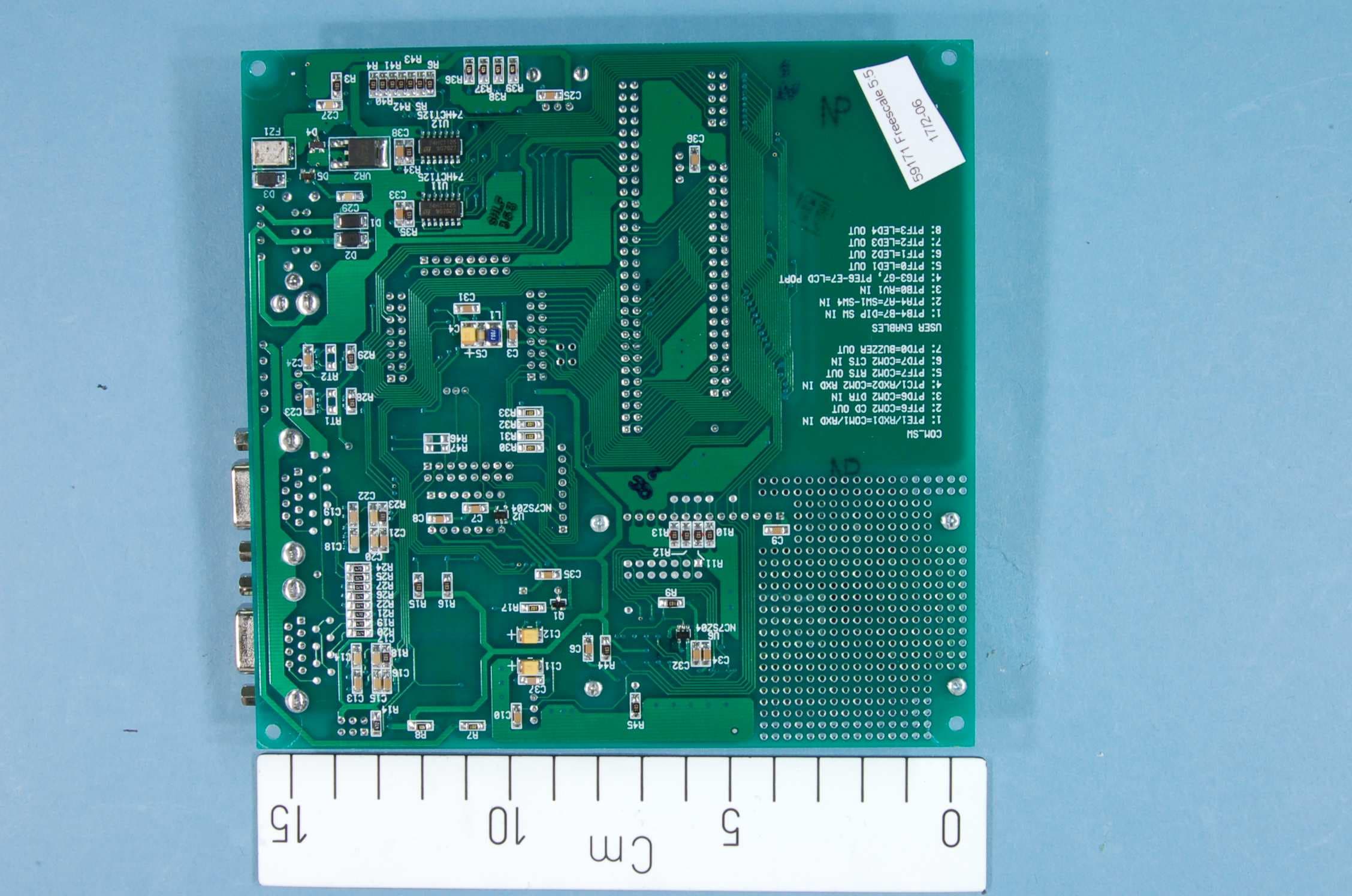
Click to zoom
Application Details
- Equipment Class
- DTS - Digital Transmission System
- Date of Grant
- Mar 15, 2006
- Application Purpose
- Original Equipment
- Date of Application
- Mar 15, 2006
- Equipment Note
- IEEE 802.15.4 Transceiver
- Frequency Range
- 2405.00000000 - 2480.00000000
- Country
- Denmark
Documents & Files
Document Text
Text extracted from the exhibit documents filed with the FCC. Open a document above to read the original.
Users Manual
MC1320x RF Daughter Card User’s Guide 1 Introduction The MC1320x RF Daughter Card, 1320xRFD-A00, is used in conjunction with a microcontroller development board for RFIC evaluation, code development, and system evaluation. It interfaces directly to the M68EVB908GB60, RG60 and QG60 HCS08 family Microcontroller Development Board and the M5223 EVB Microcontroller Development Board, but it can be adapted to other boards that offer access to the MCU input/output ports. The board is configured with all the off-chip circuitry required for functional performance of the MC1320x RF data modem except the MCU. The MCU interface required by the RFIC is pinned out at the edge of the card using standard header pins. The RF interface is accomplished through onboard antenna and can be modified for SMA connector interface. The SMA connectors can be connected to test equipment via coax cables for testing. Figure 1 Shows the RF Daughter Card. Figure 5 Shows the RF Daughter Card installed in a GB60 development board. Figure 1. MC1320xRF Daughter Card. 2 Safety Information Any modifications to this product may violate the rules of the Federal Communications Commission and make operation of the product unlawful. 47 C.F.R. Sec. 15.21 This equipment has been tested and found to comply with the limits for a Class B digital device, pursuant to part 15 of the FCC Rules. These limits are designed to provide reasonable protection against harmful interference in a residential installation. This equipment generates uses and can radiate radio frequency energy and, if not installed and used in accordance with the instructions, may cause harmful interference to radio communications. However, there is no guarantee that interference will not occur in a particular installation. If this equipment does cause harmful interference to radio or television reception, which can be determined by turning the equipment off and on, the user is encouraged to try to correct the interference by one or more of the following measures: Reorient or relocate the receiving antenna. Increase the separation between the equipment and receiver. Connect the equipment into an outlet on a circuit different from that to which the receiver is connected. Consult the dealer or an experienced radio/TV technician for help. 47 C.F.R. Sec.15.105(b) This equipment complies with FCC radiation exposure limits set forth for an uncontrolled environment. The antenna(s) used for this equipment must be installed to provide a separation distance of at least 8 inches (20cm) from all persons. This device complies with Part 15 of the FCC Rules. Operation is subject to the following two conditions: This device may not cause harmful interference. This device must accept any interference received, including interference that may cause undesired operation. 3 MCU Interface Basics Refer to the data sheet, MC1320x, and reference manual, MC1320xRM, for interface details. 4 Board Details Figure 2 shows the top side of the PCB and Figure 3 shows the bottom side. Figure 4 is the board schematic and Table 1 is the bill of materials. Referring to Figure 2 and Figure 4, connector J101 is the main interface to the M68EVB908GB60 HCS08 family Microcontroller MCU board. The interface connections fall under three broad categories; Serial Peripheral Interface (SPI), control and power. See Figure 5 for mounting. Note: MC1320x RFD J101 pin 1 need to be connected to M68EVB908GB60 GB_PORT pin 1. Referring to Figure 2 and Figure 4, connector J102 is the main interface to the M5223 EVB board. See Figure 6 for mounting. Note: MC1320x RFD J102 pin 1 need to be connected to M5223 EVB MCU_PORT pin 1. Note: All pin references in the following chapters are for the M68EVB908GB60 HCS08 family Microcontroller MCU board. Pin references in brackets are for the M5223 EVB Microcontroller MCU board. 4.1 SPI Connections J101 pins 35 through 38 (J102 pin 17, 19, 21 and 23) provide the four wire SPI interface, MOSI, SPICLK, CE, and MISO. The MC1320x always functions as a slave device. SPI operation is described in detail in the MC1320x data sheet and reference manual. Note: CE on the J102 pin 23 and 24 are wired to a header J104. This controls the functionality of CE. When the pins 2 and 3 of J104 are shunted, CE is wired to J102 pin 24 (PTE2/CE-AN7). When Pins 1 and 2 of J104 are shorted, the CE is wired to J102 pin 23 (PTE2/CE-QSPI_CS0). 4.2 Control Connections J101 Pin 19 (J102 pin 2) is the IRQ line from MC1320x. Connection to the MCU will depend on how the MCU services interrupts. RXTXEN, J101 Pin 31 (J102 Pin 20), allows the MCU to initiate transceiver functions. The ATTN line, J101 Pin 34 (J102 Pin 15), allows the MCU to wake up the MC1320x from Doze or Hibernate low power modes. RXTXEN and ATTN are also available at header J105 for manual control. J101 Pin 24 provides the MC1320x CLKO to the MCU when a jumper is installed at J103. J101 Pin 32 (J102 Pin13) interfaces with the MCU to provide a Reset to the MC1320x. J101 pins 5 and 22 can provide a wake up function to the MCU when a shunt is installed at J103. J101 pin 13 and 14 (J102 pins 9 and 11) provide access to MC1320x GPIO1 and GPIO2 ports. 4.3 Power Connections J101 pin 39(J102 pin 1) provides the supply voltage to the RF Daughter Card. Voltage on this line should never exceed 16.0 V and the nominal supply should not exceed 16.0 V. J101 pin 40 (J102 pin 3) is ground. Please note that MCU connection signals are dependant of the on-board voltage regulator. If R105, D101 and C101 is mounted, while R115 is removed, the J101 pin 39 also provides the interface supply voltage and never must exceed 3.6 V. Nominal supply should not exceed 3.4 V. 4.4 Non-MCU connections Header J105 provides connections to a number of MC1320x contacts for non MCU interface. As mentioned, RXTXEN and ATTN lines are available for external control via switches or other hardware. The MC1320x GPIO is available for interface to external hardware. 4.5 Software configuration Referring to…
Text truncated - open the document above for the full version.
External Photos
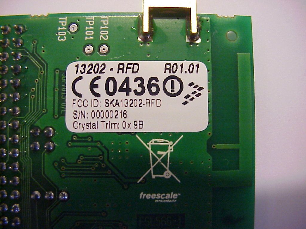
FCC ID: SKA13202RFD Project no.: 59171-3 Page 1 of 4 Nemko Comlab AS, N-2027 Kjeller PHOTOGRAPHS OF THE EUT - RFD Fig 4 - . 13202RFD- Top View Fig 5 13202RFD- rear view FCC ID: SKA13202RFD Project no.: 59171-3 Page 2 of 4 Nemko Comlab AS, N-2027 Kjeller Fig 6 - M68EVB908GB60 – Microcontroller board –Rear view Fig 7 - M68EVB908GB60 – Microcontroller board –Top view FCC ID: SKA13202RFD Project no.: 59171-3 Page 3 of 4 Nemko Comlab AS, N-2027 Kjeller Fig 8. M68EVB908GB60 – Microcontroller board – view of ports FCC ID: SKA13202RFD Project no.: 59171-3 Page 4 of 4 Nemko Comlab AS, N-2027 Kjeller PHOTOGRAPH OF THE ACCESSORIES Fig 9- . AC /DC adapter Fig 10 . RS232 cable
Internal Photos
FCC ID: SKA13202-RFD Project no.: 59171 Page 1 of 4 Nemko Comlab AS, N-2027 Kjeller PHOTOS OF THE EUT - 13202-RFD 13202-RFD- Top View 13202-RFD- rear view FCC ID: SKA13202-RFD Project no.: 59171 Page 2 of 4 Nemko Comlab AS, N-2027 Kjeller Fig 6 - M68EVB908GB60 – Microcontroller board –Rear view Fig 7 - M68EVB908GB60 – Microcontroller board –Top view FCC ID: SKA13202-RFD Project no.: 59171 Page 3 of 4 Nemko Comlab AS, N-2027 Kjeller M68EVB908GB60 – Microcontroller board – view of ports FCC ID: SKA13202-RFD Project no.: 59171 Page 4 of 4 Nemko Comlab AS, N-2027 Kjeller PHOTOS OF THE ACCESSORIES Power adaptor Fig 10 . RS232 cable
Operational Description
1 Theory of Operation 1.1 Transceiver Front-End The MC1320x RF transceiver has an RF front-end, which can be configured in two ways: • Single-port I/O with integral RX/TX switch — allows for very few external components. This is the solution that is utilized on the 13202-RFD. • Dual port with separate RX input/TX output and external switch — allows for an external LNA and/or PA. (Also allows for an external low-loss RX/TX switch.). Changing between single-port and dual-port modes is software controlled. 1.2 DC Biasing To ensure correct operation, the inputs and outputs should have the following bias: • RX inputs: Grounded. • TX outputs: Connected to VDDA This is handled automatically by the CT_Bias pin 3, such that DC bias is enabled during transmission and disabled during receive. The DC bias path is through the balun Z101 and matching network L101 – L103. 1.3 RF Matching The differential output impedance of the MC1320x is approximately 300-450 ohms and 0.6 pF in parallel. The impedance is slightly different between RX and TX. An LC-matching network steps the impedance down to 50 Ohms balanced and a small ceramic balun allows the differential to single-ended transformation. A 50:50 ohm balun is used. Although the best component values are slightly different for RX and TX, only one intermediate match L101 – L103 can be used to accommodate highest dynamic range between transmit power and receive sensitivity. Optimum procedure is to match for best RX and TX individually and then search for common components that provide acceptable performance for both modes. The low-pass LC network configuration L104 and C113 reduces TX harmonics. The center tap on the balun provides DC ground for the RX input pins and biases the TX output pins to VDDA as described in section 1.2 DC Biasing. The TX balun is RF decoupled by C112. By desolder/solder a 0 ohm resistor to another position, it is possible to select between the on-board F-antenna or the SMA connector (J100). The SMA connector may only be used for conducted RF measurements. 1.4 On-Board Antenna For ease of use, a PCB F-antenna resides on the board. The antenna bandwidth measured an approximate –10 dB return loss point at approximately 350 MHz. The resonant frequency is 2.44 GHz. • Return loss across the ISM band is better than –15 dB • The radiation pattern is omnidirectional and is very efficient • The antenna is enabled (default) 1.5 Power Supply The 13202-RFD is configured to use a 3.3 – 5.0V supply without problems by means of the on-board regulator IC102. Please note that interface logic levels will always be at 3.3V, which applies to the 13202-RFD intended usage. The MC1320x has built in voltage regulators for the internal RF circuits (1.8V nominal). RF performance is not affected by varying supply voltage and the regulators provide some noise suppression allowing less stringent supply requirements. 1.6 Reference Oscillator The MC1320x reference oscillator is a very low power oscillator to save battery consumption in Sleep and Doze Modes. The current consumption is controlled by software. The default value is 12 μA. In Doze Mode, it is possible to lower the current to 6 μA, but this sets tighter requirements on the XTAL to ensure oscillation. The Reference frequency is 16.000 MHz only. CLK0 supplies the MCU on the host board with a clock through J101 or J102. To fulfill the 802.15.4 Standard requirements, the reference frequency must be within ± 40 ppm of nominal. This includes the following: • Initial tolerance • Aging • Crystal temperature drift • Spread on the external loading capacitors The MC1321x has a built-in trimming facility that allows the initial tolerance to be calibrated out during production. For –10 to 60 °C operation, the following crystal is recommended: • KDS ZD00882 For –40 to +85 °C operation, the following crystals are recommended: • NDK (LN-G102-1341) • Toyocom (OUT1-2B-4395) • KDS (ZD01812) NOTE Some of these crystals require different values of the external loading capacitors to center the frequency. 1.7 TX Power The output power is software adjustable with a tuning range of more than 20 dB. The default power setting (Register 12: BC) is -1 dBm. This is a slight compromise between output power and current consumption. The obtainable maximum output power is 3 dBm. This setting assumes a higher current consumption can be tolerated. Tolerance: ±1 dBm The 802.15.4 Standard requirement is greater than -3 dBm. 1.8 Harmonics 2nd harmonic is typically -40 dBm or lower. 3rd harmonic is low, but does not exceed -60 dBm. The 802.15.4 Standard requirement is less than -30 dBm 1.9 RX Sensitivity Sensitivity was measured at -95 dBm, ±2 dBm (1% PER, 20 byte payload). The 802.15.4 Standard requirement is less than -85 dBm.
Test Report
Nemko AS, Gaustadalléen 30, P.O.Box 73 Blindern, NO-0314 Oslo Norway T +47 22 96 03 30 F +47 22 96 05 50 Enterprise number NO974404532 Visiting address: Nemko Comlab Gåsevikveien 8, P.O.Box 96, NO-2027 Kjeller Norway T +47 64 84 57 00 F +47 64 84 57 05 No of Pages : 34 Test report # : 59171-3 Item tested : 13202-RFD Type of equipment : IEEE 802.15.4, 2.4GHz (Daughter card) FCC ID : SKA13202-RFD Client : Freescale Semiconductor Denmark AS Tested according to : FCC part 15.247 Digital Transmission System Date of issue : 9 March 2006 Authorized by : ............ ................................... Frode Sveinsen Technical Verificator FCC part 15C Test Report Project no. : 59171 FCC ID: SKA13202-RFD Nemko Comlab, Kjeller, Norway Page 2 (34) CONTENTS 1 GENERAL INFORMATION....................................................................................................3 1.1 Testhouse Info .............................................................................................................3 1.2 Client Information .........................................................................................................3 1.3 Manufacturer ................................................................................................................3 2 Test Information .....................................................................................................................4 2.1 Test Item ......................................................................................................................4 2.2 Test Environment .........................................................................................................5 2.3 Test Period...................................................................................................................5 3 TEST REPORT SUMMARY...................................................................................................6 3.1 General ........................................................................................................................6 3.2 Test Summary..............................................................................................................7 3.3 Description of modification for Modification Filing .......................................................7 3.4 Comments....................................................................................................................7 3.5 Family List Rational......................................................................................................7 4 TEST RESULTS.....................................................................................................................8 4.1 Powerline Conducted Emissions .................................................................................8 4.2 Bandwidth ..................................................................................................................10 4.3 Peak Power Output....................................................................................................13 4.4 Spurious Emissions (Radiated) .................................................................................16 4.5 Power Spectral Density (PSD)...................................................................................29 5 LIST OF TEST EQUIPMENT ...............................................................................................32 6 BLOCK DIAGRAM ...............................................................................................................33 6.1 System set up ............................................................................................................33 6.2 Powerline Conducted Emission .................................................................................33 6.3 Test Site Radiated Emission......................................................................................34 FCC part 15C Test Report Project no. : 59171 FCC ID: SKA13202-RFD Nemko Comlab, Kjeller, Norway Page 3 (34) 1 GENERAL INFORMATION 1.1 Testhouse Info Name : Nemko Comlab Address : Gåsevikveien 8, Box 96 N-2027 Kjeller, NORWAY Telephone : +47 64 84 57 00 Fax : +47 64 84 57 05 E-mail: [email protected] FCC test firm registration # : 994405 Industry Canada OATS registration # : 4443 1.2 Client Information Name : Freescale Semiconductor Danmark A/S Address : Skalhuse 5, 9240 Nibe, Denmark Telephone : +45 967 10 000 Fax : +45 983 50 052 Contact: Name : Flemming Nygaard Telephone : +45 7024 14 65 E-mail : [email protected] 1.3 Manufacturer Name : Freescale Semiconductor Danmark A/S Address : Skalhuse 5, 9240 Nibe, Denmark Telephone : +45 967 10 000 Fax : +45 983 50 052 FCC part 15C Test Report Project no. : 59171 FCC ID: SKA13202-RFD Nemko Comlab, Kjeller, Norway Page 4 (34) 2 Test Information 2.1 Test Item Name : 13202-RFD FCC ID : SKA13202-RFD Model/version : 13202-RFD Serial number : Marked as “Cond 7” & “Rad 8” Hardware identity and/or version: 80000566000_R0100 Software identity and/or version : PTC version 2.10 RFD Frequency Range : 2405 – 2480 MHz Tunable Bands : 1 Number of Channels : 16 1 Operating Modes : TX & RX Type of Modulation : O-QPSK Emissions Designator : G1D User Frequency Adjustment : None, Software controlled Rated Output Power : 2 mW Type of Power Supply : AC mains adapter ( out put voltage 9Vdc) Antenna Connector : Integral antenna (SMA connector only for testing purpose) Antenna Diversity Supported : None 1) 16 channels in use. Theory of Operation The MC13202 RF transceiver is an IEEE® 802.15.4-compliant radio that operates in the 2.4 GHz ISM frequency band. This daughter card (RFD) is mounted on M68EVB908GB60. The M68EVB908GB60 single board computer is a fully assembled, fully functional development board for the Freescale M9S08GB60 microcontroller. Provided with wall plug power supply and serial cable. Support software for this development board is provided for Windows 95/98/NT/2000/XP operating systems. Description of Test It…
Text truncated - open the document above for the full version.
Test Setup Photos
FCC ID: SKA13202-RFD Project no.: 59171 Page 1 of 2 Nemko Comlab AS, N-2027 Kjeller PHOTOS OF TEST SET-UP 13202-RFD - Radiated emission 9 kHz – 25 GHz 13202-RFD - Conducted measurements FCC ID: SKA13202-RFD Project no.: 59171 Page 2 of 2 Nemko Comlab AS, N-2027 Kjeller 13202-RFD - Conducted emission test set-up
Contact Information
Applicant
Johnny Jonassen(R&D Engineer)
Test Firm
Nemko ASFrode Sveinsen
Technical Specifications
| # | Rule Parts | Frequency Range | Power Output |
|---|---|---|---|
| 1 | 15C | 2.40 GHz - 2.48 GHz | 2.00 mW |
Other Applications from Freescale Semiconductor Danmark A/S
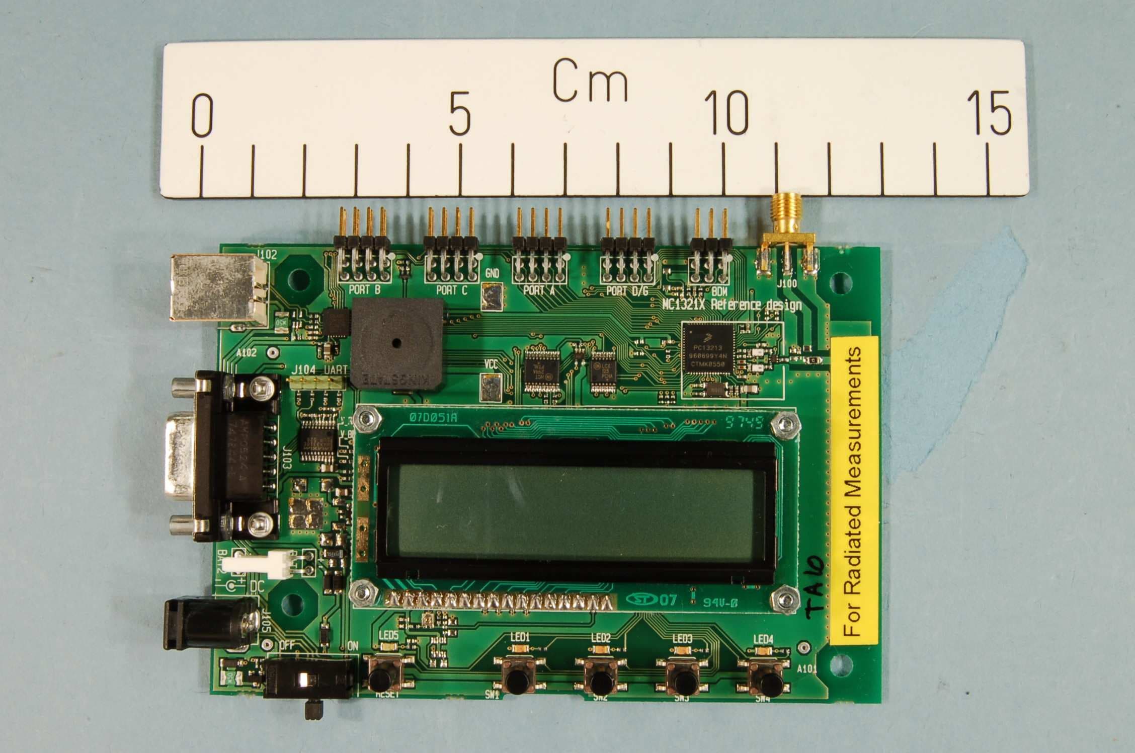
SKA13213-NCB
Mar 08, 2006IEEE 802.15.4 Transceiver
Equipment Class
DTS - Digital Transmission System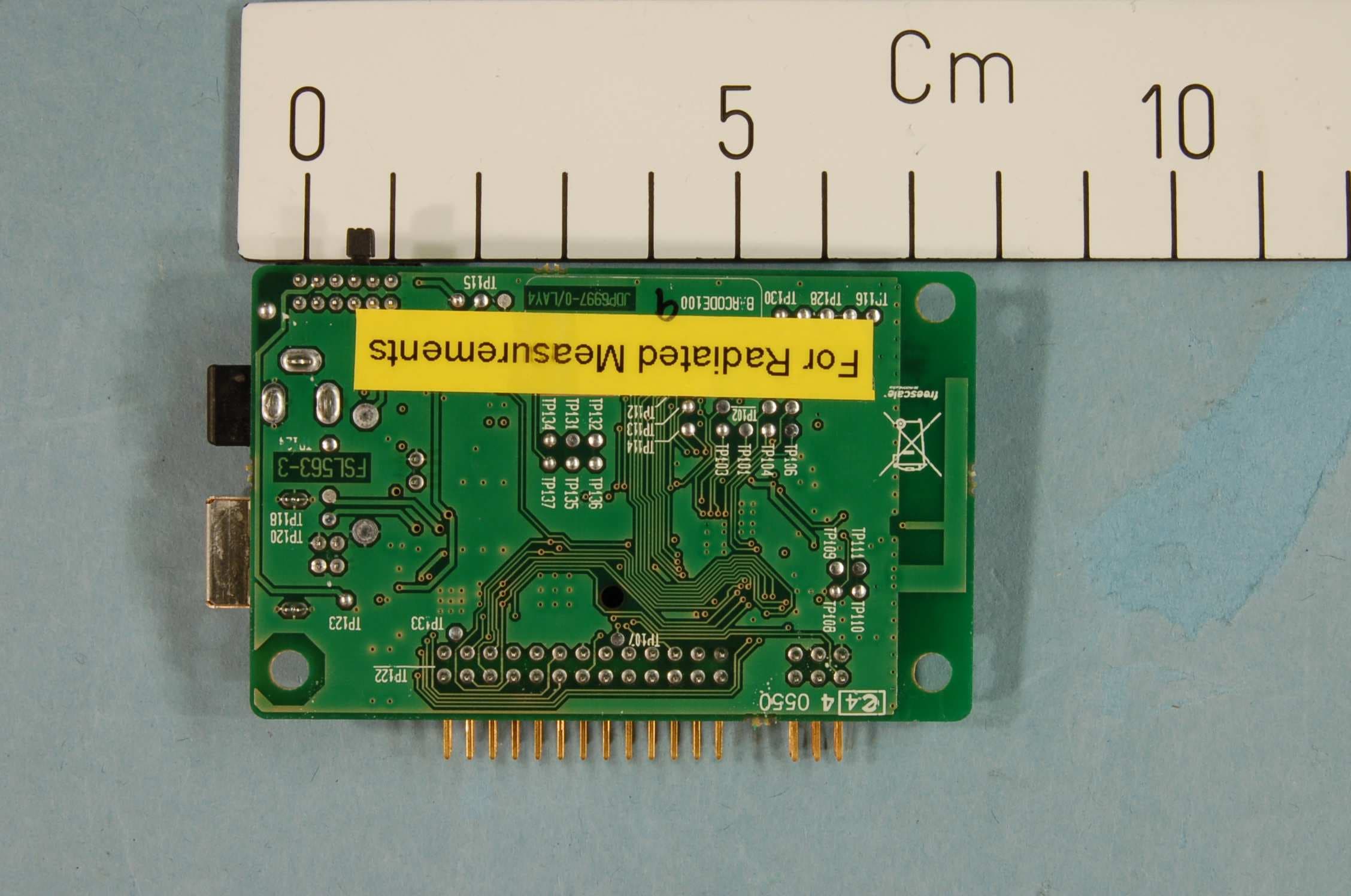
SKA13213-SRB
Mar 08, 2006IEEE 802.15.4
Equipment Class
DTS - Digital Transmission System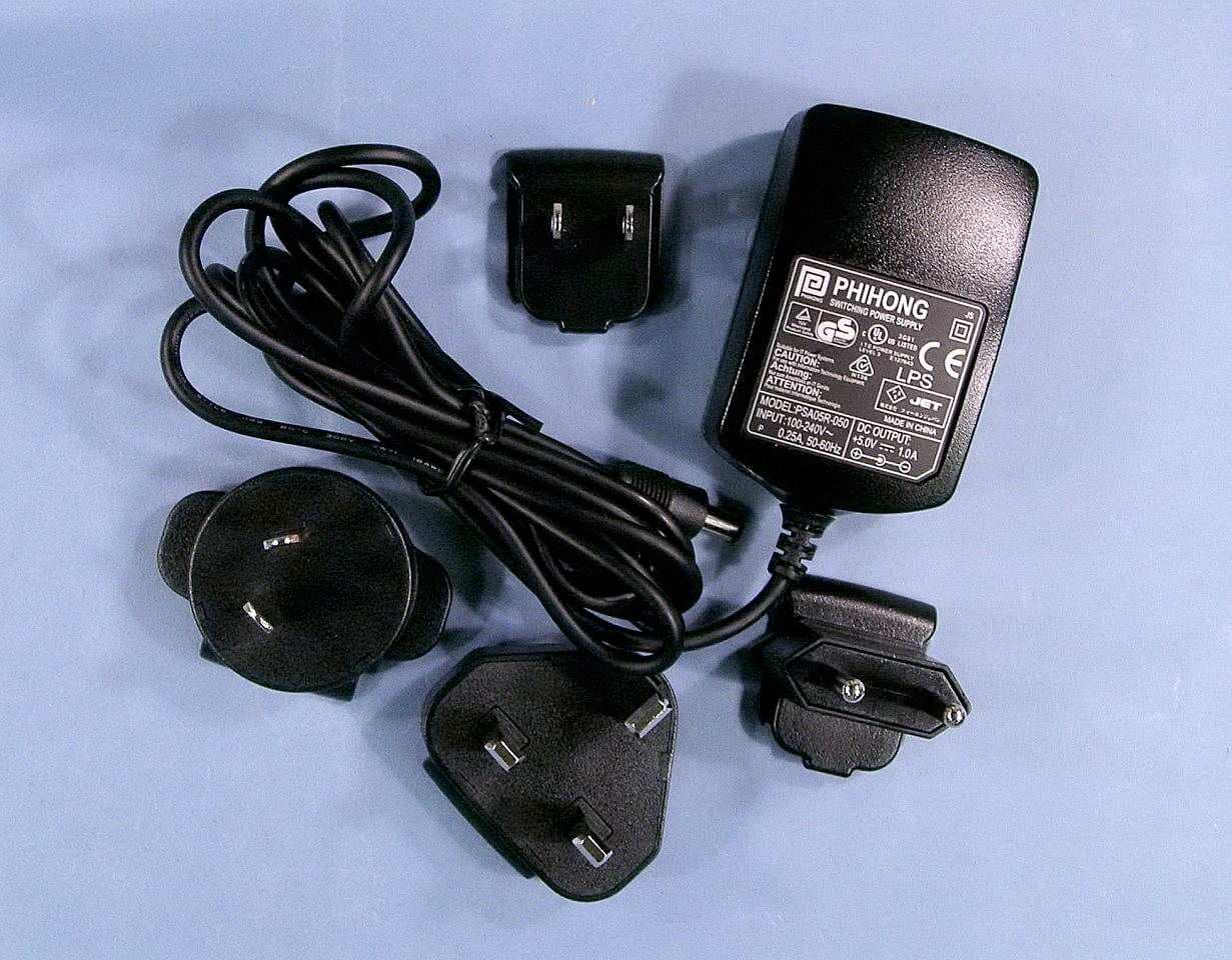
SKA13192-SARD
Mar 07, 2005DTS Transceiver
Equipment Class
DTS - Digital Transmission System