SKUEPP100IJWUS Charger Pad
DONGYANG E&P Inc.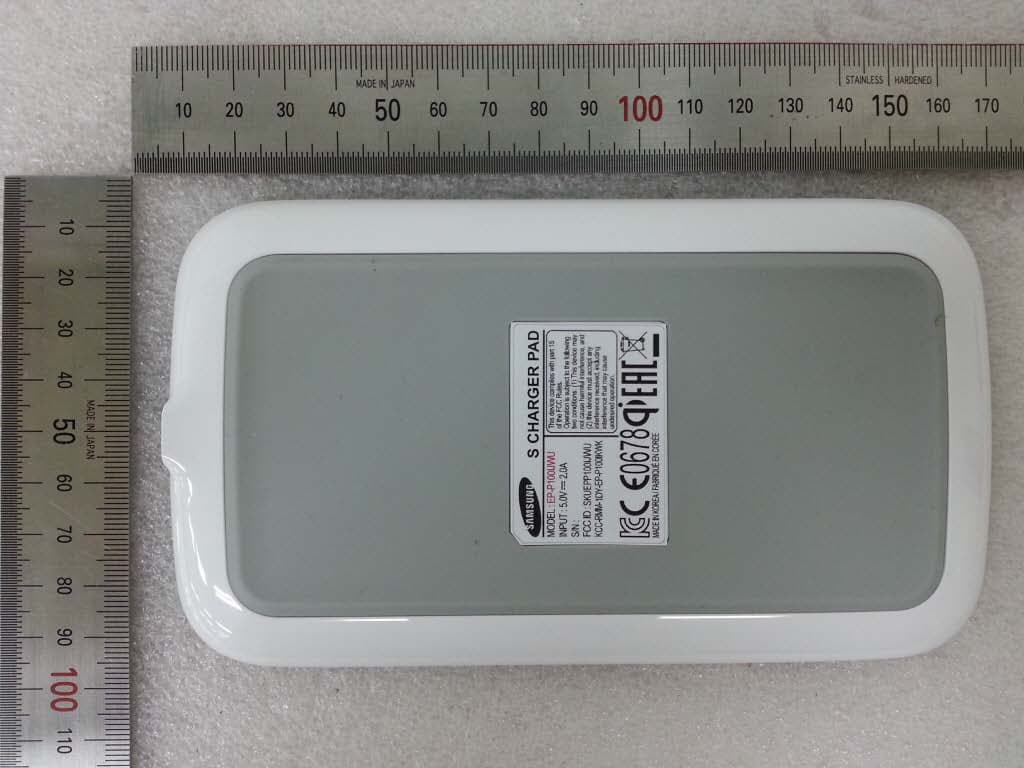
Click to zoom
Application Details
- Equipment Class
- DCD - Part 15 Low Power Transmitter Below 1705 kHz
- Date of Grant
- Jun 05, 2013
- Application Purpose
- Original Equipment
- Date of Application
- Jun 05, 2013
- Equipment Note
- S Charger Pad
- Frequency Range
- 0.11200000 - 0.20500000
- Company
- DONGYANG E&P Inc.
- Country
- South Korea
Documents & Files
Document Text
Text extracted from the exhibit documents filed with the FCC. Open a document above to read the original.
Users Manual
Type B. A00103 04/2013. Rév. 1.0www.samsung.com English Safety information To prevent injury to yourself and others or damage to your device, read the safety information about your device before using the device Samsung cannot be held responsible for any injury or property damage caused by failure to comply with the safety cautions and regulations Do not use damaged power cords or plugs, or loose electrical sockets Do not touch the power cord with wet hands or disconnect the charger by pulling the cord Do not bend or damage the power cord Do not store your device with metal objects, such as coins, keys, and necklaces Your device may overheat. Do not use your device or applications for a while if the device is overheated Prolonged exposure of your skin to an overheated device may cause low temperature burn symptoms, such as red spots and pigmentation. Do not store your device near or in heaters, microwaves, hot cooking equipment, or high pressure containers Your device may overheat and cause a fire. Do not drop or cause an impact to the charger or the device Store your device only on flat surfaces• If your device falls, it may be damaged.• Do not bite or suck the device or the battery Doing so may damage the device or cause an explosion.• If children use the device, make sure that they use the • device properly. Keep your device dry Humidity and liquids may damage the parts or electronic • circuits in your device. If your device is wet, dry the device with a towel and take it • to a service center. Do not disassemble, modify, or repair your device Your device may malfunction and your risk of electric • shock is increased. Any changes or modifications to your device can void your • manufacturer’s warranty. If your device needs servicing, take your device to a Samsung Service Center. This manual’s images and content may differ from the product. Overview Check the product box for the following items: Wireless Charging Pad and user manual. The items supplied with the Wireless Charging Pad and any available accessories may vary depending on the region. Using the Wireless Charging Pad Connect the Wireless Charging Pad and a charger 1 with a charging cable, and plug the charger into an electric socket. When the Wireless Charging Pad is connected to the • electric socket, the indicator light flashes from red to green to orange, and then turns off. Use only Samsung-approved chargers (over 2 A). Unauthorized chargers may cause damage or the Wireless Charging Pad may malfunction. The charger and the charging cable are sold • separately. The Wireless Charging Pad’s indicator light flashes • differently depending on its status. For more information about the indicator light, see below. If the indicator light is not working properly, reconnect the charger to the Wireless Charging Pad. Indicator lightDevice status Red → Green → Orange When connecting to the power outlet OrangeWhen not charging properly GreenWhen charging properly OffWhen in Idle mode Attach the Wireless Charging Cover to a 2 smartphone, and then place the smartphone on the Wireless Charging Pad. The Wireless Charging Cover is sold separately. For more information about the Wireless Charging Cover, refer to the Wireless Charging Cover’s user manual. When the smartphone is fully charged, disconnect 3 the charger from the Wireless Charging Pad. Check the smartphone’s battery status looking at • the charging icon displayed on the screen. Do not place any other object between the • smartphone and the Wireless Charging Pad. The smartphone may not charge properly. Charging a smartphone with the Wireless Charging • Pad in an area with a weak signal may cause a significant drop in reception. The Wireless Charging Pad is compatible with WPC • certified devices. Do not place the Wireless Charging Cover solely on the Wireless Charging Pad Doing so may overheat the device and cause a fire. Place the smartphone properly on the Wireless Charging Pad The position guide indicates the upper side, lower side and the center of the Wireless Charging Pad. Match the upper and lower side of the smartphone with the Wireless Charging Pad, and place the smartphone in the middle. If not, the smartphone may not charge properly, and its signal may drop. FCC This device complies with part 15 of the FCC Rules. Operation is subject to the following two conditions: (1) This device may not cause harmful interference, and (2) this device must accept any interference received, including interference that may cause undesired operation. Users are not permitted to make changes or modify the device in any way. Changes or modifications not expressly approved by Samsung will void the user’s authority to operate the equipment. Based on Wireless charging standards, must keep the device at least 10 cm away from user during usage. Position guide Indicator light Charging jack Tapis de recharge sans fil S Charger Pad Wireless Charging Pad IC This device complies with Industry Canada licence-exempt RSS standard(s). Operation is subject to the following two conditions: (1) this device may not cause interference, and (2) this device must accept any interference, including interference that may cause undesired operation of the device. EP-P100_UM_B.indd 12013-04-25 오전 11:45:33 Français Consignes de sécurité Afin d’éviter de blesser votre entourage ou vous-même, ou bien d’endommager votre appareil, veuillez lire toutes les consignes de sécurité au sujet de l’appareil avant de l’utiliser Samsung ne peut pas être tenu responsable de toute blessure ou de tout dommage matériel lié au non respect des avertissements de sécurité et des réglementations Ne pas utiliser de fiches ou de cordons d’alimentation endommagés, ou de prises électriques mal fixées Ne pas toucher le cordon d’alimentation lorsque vos mains sont mouillées et ne pas tirer sur le cordon pour débrancher le chargeur Ne pas tordre ou endommager le cordon d’alimentation Ne pas ranger l’appareil avec des objets métalliques, comme de la…
Text truncated - open the document above for the full version.
Cover Letter(s)
31B 3-1, Jinwi Industrial Estate, Cheongho-Ri, Jinwi-Myeon, Pyeongtaek-Si, Gyeonggi-Do, South Korea Tel : +82-31-370-6801 Fax : +82-31-233-9090 Date (21/05/2013) BABT FCB Forsyth House, Churchfield Road, Walton-on-Thames, Surrey, KT12 2TD Dear Sir or Madam, We, DONGYANG E&P Inc. : 31B 3-1, Jinwi Industrial Estate, Cheongho-Ri, Jinwi-Myeon, Pyeongtaek-Si, Gyeonggi-Do, 451-862, Korea, hereby authorize Young-Joon, Park (CTK Co., Ltd. : 386-1, Ho-dong, Cheoin-gu, Yongin-si, Gyeonggi-do, Korea) to act as our agent in all matters relating to applications for equipment authorization, including the signing of all documents relating to these matters. This authorization expires on 21/05/2014. Sincerely, Company Officer: Jin-bum, Kim Telephone Number: +82-31-370-6801 Email: [email protected]
Cover Letter(s)
31B 3-1, Jinwi Industrial Estate, Cheongho-Ri, Jinwi-Myeon, Pyeongtaek-Si, Gyeonggi-Do, South Korea Tel : +82-31-370-6801 Fax : +82-31-233-9090 Date (21/05/2013) BABT TCB Forsyth House, Churchfield Road, Walton-on-Thames, Surrey, KT12 2TD Confidentiality Request FCC ID: SKUEPP100IJWU Pursuant to Sections 0.457(d)(1)(ii) and 0.459 of the Commission’s Rules, DONGYANG E&P Inc. hereby requests permanent confidential treatment of information accompanying this application as outlined below: Schematics Bill of Materials/Parts List Block Diagrams Theory of Operation DONGYANG E&P Inc. also hereby requests short-term confidential treatment of information accompanying this application as outlined below for a period of 0 day: [Common exhibits for which short-term confidentiality is requested are: Internal Photos External Photos User Manual Test Set-up Photographs The above materials contain trade secrets and proprietary information not customarily released to the public. The public disclosure of these matters might be harmful to the Applicant and provide unjustified benefits to its competitors. The Applicant understands that pursuant to Rule 0.457(d)(1)(ii), disclosure of this Application and all accompanying materials will not be made before the date of the Grant for this Application. Yours sincerely, Company Officer: Jin-bum, Kim Telephone Number: +82-31-370-6801 Email: [email protected]
External Photos
CTK Co., Ltd. 386-1, Ho-dong, Cheoin-gu, Yongin-si, Gyeonggi-do, 449-100, Korea Tel: +82-31-339-9970 Fax: +82-31-339-9855 www.e-ctk.com Page 1 of 1 EUT External Photos
ID Label/Location Info
CTK Co., Ltd. 386-1, Ho-dong, Cheoin-gu, Yongin-si, Gyeonggi-do, 449-100, Korea Tel: +82-31-339-9970 Fax: +82-31-339-9855 www.e-ctk.com Page 1 of 1 EUT Label Photos
Internal Photos
CTK Co., Ltd. 386-1, Ho-dong, Cheoin-gu, Yongin-si, Gyeonggi-do, 449-100, Korea Tel: +82-31-339-9970 Fax: +82-31-339-9855 www.e-ctk.com Page 1 of 3 EUT Internal Photos CTK Co., Ltd. 386-1, Ho-dong, Cheoin-gu, Yongin-si, Gyeonggi-do, 449-100, Korea Tel: +82-31-339-9970 Fax: +82-31-339-9855 www.e-ctk.com Page 2 of 3 CTK Co., Ltd. 386-1, Ho-dong, Cheoin-gu, Yongin-si, Gyeonggi-do, 449-100, Korea Tel: +82-31-339-9970 Fax: +82-31-339-9855 www.e-ctk.com Page 3 of 3
Parts List/Tune Up Info
NoCODE(업체명)ComponentMtr. TypeDESCRIPTONLOCATIONO.QTYVENDORWEIGHT/UNIT SMD 1 MRNAA038910PCBPCBFR-4, 4 Layer, 1.0T, H/F, 155*201, 2*4연배-1FINE CIRCUIT 2 MQCAD027180 CapacitorMLCC GRM188R71H104KA93D / 0.1uF 50V X7R 1608 C5,C26,C33,C41,C42, C43,C45,C47,C48,C52, C55 11MURATA 3 MQCAD024540 CapacitorMLCC C CRM 0402F104Z160C / 16V 100nF Z 1005C691WALSIN 4 MQCAD027030 CapacitorMLCC C1608X7R1E105K / 1uF 25V X7R 1608 C3,C10,C11C29,C30, C31 6TDK 5 MQCAD027040 CapacitorMLCC GRM219R61E106KA12D / 10uF 25V X5R 2012C61MURATA 6 MQCAD027050 CapacitorMLCC C1005X7R1H682K / 6.8nF 50V X7R 1005C181TDK 7 MQCAD027190 CapacitorMLCC GRM188R71H332JA01D / 3.3nF 50V X7R 1608C191MURATA 8 MQCAD027070 CapacitorMLCC C1608X7R2A332K / 3.3nF 100V X7R 1608C281TDK 9 MQCAD027080 CapacitorMLCC C1005X7R1H102KT / 1nF 50V X7R 1005C24,C53,C543TDK 10 MQCAD027090 CapacitorMLCC GRM32ER71E226KE15L / 22uF 25V X7R 3225C17,C46 2MURATA 11 MQCAD027100 CapacitorMLCC GRM155R71H223KA12D / 22nF 50V X7R 1005C271MURATA 12 MQCAD027200 CapacitorMLCC GRM31M5C1H473JA01L / 47nF 50V C0G 3216C50,C512 MURATA 13 MQCAD027210 CapacitorMLCC GRM31C5C1H104JA01L / 100nF 50V C0G 3216C20,C21, C22,C254 MURATA 14 MQCAD027150 CapacitorMLCC GRM1555C1H101JA01D / 100pF 50V C0G 1005C601MURATA 15 MQCAD027160 CapacitorMLCC GRM155R71H472KA01D / 4.7nF 50V X7R 1005C11MURATA 16 MPBAA005270 S/W DIODES/W DIODE-SMD BAV21W-7-F / SOD-123, 250V, 400mA, 250mW, 50nSD61DIODES 17 MPBAA004920 S/W DIODES/W DIODE-SMD 1N4148W-7-F / SOD-123, 75V 300mA,D51성호반도체 18 MQAAG083730 Resistor R-CHIPWR04X473FTL / 47K Ω 1/16W F, 1005R27,R70, R1083WALSIN 19 MQAAG082760 Resistor R-CHIPWR04X472JTL / 4.7K Ω 1/16W J, 1005R971WALSIN 20 MQAAG083080 Resistor R-CHIPWR04X1002FTL / 10K Ω 1/16W F, 1005 R17,R30,R32,R93,R98, R119,R121,R100 8WALSIN 21 MQAAG083590 Resistor R-CHIPWR04X2701FTL / 2.7K Ω 1/16W F, 1005R33, R342WALSIN 22 MQAAG082680 Resistor R-CHIPWR04X1003FTL / 100K Ω 1/16W F, 1005R381WALSIN 23 MQAAG087820 Resistor R-CHIPWR06X152JTL / 1.5K Ω 1/10W J, 1608R311WALSIN 24 MQAAG065250 Resistor R-CHIPWR06X153FTL / 15K Ω 1/10W F, 1608R411WALSIN 25 MQAAG064960 Resistor R-CHIPWR06X200FTL / 20 Ω 1/10W F, 1608R77,R782WALSIN 26 MQAAG087760 Resistor R-CHIPWW12XR020FTL / 0.02 Ω 1/4W F, 3216R861WALSIN 27 MQAAG087850 Resistor R-CHIPWR04X1200FTL / 120 Ω 1/16W F, 1005R101WALSIN 28 MQAAG087860 Resistor R-CHIPWR04X3600FTL / 360 Ω 1/16W F, 1005R61WALSIN 29 MQAAG087770 Resistor R-CHIPWR06X3600FTL / 360 Ω 1/10W F 1608R73,R74,R75,R804WALSIN 30 MQAAG087800 Resistor R-CHIPWR06W3R30FTL / 3.3 Ω 1/10W F, 1608R76,R79,R853WALSIN 31 MQAAG087780 Resistor R-CHIPWR04X10R0FTL / 10 Ω 1/16W F, 1005R821WALSIN 32 MQAAG087790 Resistor R-CHIPWR04X2400FTL / 240 Ω 1/16W F, 1005R811WALSIN 33 MQAAG082840 Resistor R-CHIPWR04X101JTL / 100 Ω 1/16W J, 1005R84,R87,R1253WALSIN 34 MQAAG063400 Resistor R-CHIPWR04X151JTL / 150 Ω 1/16W J, 1005R881WALSIN 35 MQAAG088100 Resistor R-CHIPWR04X4992FTL / 49.9K Ω 1/16W F, 1005R901WALSIN 36 MQAAG087840 Resistor R-CHIPWR04X1004FTL / 1M Ω 1/16W F, 1005R1241WALSIN 37 MQAAG087870 Resistor R-CHIPWR04X2202FTL / 22K Ω 1/16W F, 1005R1221WALSIN 38 MQAAG087880 Resistor R-CHIPWR04X4022FTL / 40.2K Ω 1/16W F, 1005R141WALSIN 39 MQAAG087890 Resistor R-CHIPWR04X6801FTL / 6.8K Ω 1/16W F, 1005R51WALSIN 40 MQAAG087900 Resistor R-CHIPWR04X3301FTL / 3.3K Ω 1/16W F, 1005R891WALSIN 41 MPDAA006660LED LED -SMD LG-195HRF/9UG-CT-2 / Red, Green Dual LEDD11LIGITEK 42 MPHAC000010 IC-ANLOG MUTIPLEXER IC-ANLOG MUTIPLEXER -SMD IDTP9035 / TQFN48, 5V, 20mAU11IDT 43 MPCAE013580IC-FETIC-FET-SMDNCP349MNBKTBG / DFN6, NMOS, UVLO 3.25V, OVLO 6.4V U21Onsemi 44 MPIAB000080IC-EEPROM IC-EEPROM-SMD CAT24C64 / TSSOP8, EEP ROM, 5 V, 1mA, CMOS, 64KbU31Onsemi 45 MPFAC001260IC-TTL TTL-SMD 74LVC2G74DP / SOT505-2, TTL, 5V 300mW 100mAU41NXP 46 MPFAA000040IC-CMOS LOGIC IC-CMOS LOGIC-SMD 74AHC2G08DP / SOT505-2, 5V 250mW 75mAU101NXP 47 MPHAT000010IC-FET DRIVER IC-FET DRIVER -SMD TC4428COA / MSOP8, 4.5V to 18V, 340mW, U14,U162Microchip 48 MPJAK005190IC-AMP IC-AMP-SMD AD8541ARTZ / SOT23, 5 V , 45uAU121Analog Devices 49 MPCAE013540 IC-FET IC-FET-SMD SiA445EDJ-T1-GE3 / SC70, 20 V, 12A, 19WQ6,Q82VISHAY 50 MPCAE013550IC-FET IC-FET-SMD SiA400EDJ-T1-GE3 / SC70, 30 V, 12A, 19.2WQ5,Q72VISHAY 51 MPCAA010420TRTR-SMDBC857CLT1G / SOT23_3, PNP, -45V, -100mA, 225mWQ91NXP 52 MPCAE012400FET FET-SMD 2N7002 / SOT23_3, 60 V, 300 mAQ4, Q14, Q153KEC 53 MRBAA000010EMI FilterEMI Filter-SMDDLW5BTM251SQ2L / LINEFILTER_SDLF0502101YN,L21MURATA 54 MRJAK025260USB CONNECTOR-SMD GU07D-7P-SB-E1500 / MICRO USB Standard TYPE 4DIPJ21LSMtron 수삽 55 MQIAB004400THERMISTOR THERMISTOR-Hand Insert RBS103F3435F01 AO20 / LEAD TYPE, 10KΩ, FTH11JOINSET 56 MQHAH000070COIL COIL-ETC CEBO-PA0R16AL11Chemtronics 부자재 57 MFBAC000220 Cream SolderCream Solder M705-GRN360-K2-V / LEAD FREE -1 SENJU0.016g 58 MFBAB001030 SOLDER WIRE SOLDER WIRE-Subsidiary materials HSE-04 0.8Φ / SR34-SUPER(LFM32 3.5%) -1 희성소재0.6505g EP-P100IJWU Part list
RF Exposure Info
CTK Co., Ltd. 386-1, Ho-dong, Cheoin-gu, Yongin-si, Gyeonggi-do, 449-100, Korea Tel: +82-31-339-9970 Fax: +82-31-339-9855 www.e-ctk.com Test Report No.: CTK-2013-00857-1 Date: May 27, 2013 Page 1 of 12 This Report shall not be reproduced except in full without the written approval of CTK Form No.: CTK-RF-EF-Part15 Subpart C(Rev.1) RF EXPOSURE REPORT According to : FCC 47CFR part 1 subpart I and part 2 subpart J Test Report No. : CTK-2013-00857-1 Date of Issue : May 27, 2013 FCC ID : SKUEPP100IJWU Equipment Under Test : EP-P100IJWU Kind of Product : S Charger Pad Applicant : DONGYANG E&P Inc. Applicant Address : 31B 3-1, Jinwi Industrial Estate, Cheongho-Ri, Jinwi-Myeon, Pyeongtaek-Si, Gyeonggi-Do, 451-862, Korea Manufacturer : DONGYANG E&P Inc. Manufacturer Address : 31B 3-1, Jinwi Industrial Estate, Cheongho-Ri, Jinwi-Myeon, Pyeongtaek-Si, Gyeonggi-Do, 451-862, Korea Contact Person : Jin-bum, Kim / Project Manager Telephone : +82-31-370-6801 Received Date : May 7, 2013 Test period : Start : May 7, 2013 End : May 21, 2013 Test Results : In Compliance Not in Compliance The test results presented in this report relate only to the object tested. Tested by Reviewed by Young-taek Lee Test Engineer Young-Joon, Park Technical Manager Date: May 27, 2013 Date: May 27, 2013 CTK Co., Ltd. 386-1, Ho-dong, Cheoin-gu, Yongin-si, Gyeonggi-do, 449-100, Korea Tel: +82-31-339-9970 Fax: +82-31-339-9855 www.e-ctk.com Test Report No.: CTK-2013-00857-1 Date: May 27, 2013 Page 2 of 12 This Report shall not be reproduced except in full without the written approval of CTK Form No.: CTK-RF-EF-Part15 Subpart C(Rev.1) REPORT REVISION HISTORY Date Revision Page No May 21, 2013 Issued (CTK-2013-00857) All May 27, 2013 Issued (CTK-2013-00857-1) Update 2.1 Test Setup All This report shall not be reproduced except in full, without the written approval of CTK Co., Ltd. This document may be altered or revised by CTK Co., Ltd. personnel only, and shall be noted in the revision section of the document. Any alteration of this document not carried out by CTK Co., Ltd. will constitute fraud and shall nullify the document. CTK Co., Ltd. 386-1, Ho-dong, Cheoin-gu, Yongin-si, Gyeonggi-do, 449-100, Korea Tel: +82-31-339-9970 Fax: +82-31-339-9855 www.e-ctk.com Test Report No.: CTK-2013-00857-1 Date: May 27, 2013 Page 3 of 12 This Report shall not be reproduced except in full without the written approval of CTK Form No.: CTK-RF-EF-Part15 Subpart C(Rev.1) TABLE OF CONTENTS REPORT REVISION HISTORY .......................................................................................... 2 1.0 General Product Description ............................................................................... 4 1.1 Model Differences ............................................................................................. 4 1.2 Device Modifications ......................................................................................... 4 1.3 Peripheral Devices ............................................................................................ 4 1.4 EUT Operating Modes ........................................................................................ 5 1.5 Test Modes ...................................................................................................... 5 1.6 Calibration Details of Equipment Used for Measurement ......................................... 7 1.7 Test Facility...................................................................................................... 7 1.8 Laboratory Accreditations and Listings ................................................................. 7 2.0 Summary of tests ............................................................................................. 8 2.1 Test Setup ....................................................................................................... 9 2.2 Radiofrequency radiation exposure limits ........................................................... 10 2.3 Test Results ................................................................................................... 11 APPENDIX A – Test Equipment Used For Tests ................................................................ 12 CTK Co., Ltd. 386-1, Ho-dong, Cheoin-gu, Yongin-si, Gyeonggi-do, 449-100, Korea Tel: +82-31-339-9970 Fax: +82-31-339-9855 www.e-ctk.com Test Report No.: CTK-2013-00857-1 Date: May 27, 2013 Page 4 of 12 This Report shall not be reproduced except in full without the written approval of CTK Form No.: CTK-RF-EF-Part15 Subpart C(Rev.1) 1.0 General Product Description Type of equipment S Charger Pad Equipment model name EP-P100IJWU Frequency Range 112 kHz – 205 kHz Antenna type Coil antenna Power Source TRAVEL ADAPTER Input : AC 100-240 V, 50/60 Hz Output : DC 5 V, 2.0 A Test Voltage and Frequency : AC 120 V, 60 Hz 1.1 Model Differences Not applicable 1.2 Device Modifications The following modifications were necessary for compliance: Not applicable 1.3 Peripheral Devices Device Manufacturer Model No. Serial No. FCC ID or DoC TRAVEL ADAPTER TIANJIN E&P ELECTRONICS Inc. ETA-U90KWK DK3D301TS/B-E Verification Wireless Charging Cover RFTech Co., Ltd. EBC-1G6WWE RT0C802AS/4-E - Mobile Phone Samsung Electronics Co., Ltd. SCH-I535 - A3LSCHI535 CTK Co., Ltd. 386-1, Ho-dong, Cheoin-gu, Yongin-si, Gyeonggi-do, 449-100, Korea Tel: +82-31-339-9970 Fax: +82-31-339-9855 www.e-ctk.com Test Report No.: CTK-2013-00857-1 Date: May 27, 2013 Page 5 of 12 This Report shall not be reproduced except in full without the written approval of CTK Form No.: CTK-RF-EF-Part15 Subpart C(Rev.1) 1.4 EUT Operating Modes Equipment under test was operated during the measurement under the following conditions: Charging and communication mode Modulation Type : CW (Continuous Wave) Output Power : Max. 5.49 dBuV/m (Frequency 119.34 kHz, Test Distance 3 m) TX Duty Cycle : 100 % by measurement 1.5 Test Modes This device has been tested below conditions: [Test Mode #1] Frequency Charging current Note 112 kHz 650 mA L…
Text truncated - open the document above for the full version.
Test Report
CTK Co., Ltd. 386-1, Ho-dong, Cheoin-gu, Yongin-si, Gyeonggi-do, 449-100, Korea Tel: +82-31-339-9970 Fax: +82-31-339-9855 www.e-ctk.com Test Report No.: CTK-2013-00856 Date: May 21, 2013 Page 1 of 30 This Report shall not be reproduced except in full without the written approval of CTK Form No.: CTK-RF-EF-Part15 Subpart C(Rev.1) TEST REPORT According to : FCC 47CFR part 15 subpart C Test Report No. : CTK-2013-00856 Date of Issue : May 21, 2013 FCC ID : SKUEPP100IJWU Equipment Under Test : EP-P100IJWU Kind of Product : S Charger Pad Applicant : DONGYANG E&P Inc. Applicant Address : 31B 3-1, Jinwi Industrial Estate, Cheongho-Ri, Jinwi-Myeon, Pyeongtaek-Si, Gyeonggi-Do , 451-862, Korea Manufacturer : DONGYANG E&P Inc. Manufacturer Address : 31B 3-1, Jinwi Industrial Estate, Cheongho-Ri, Jinwi-Myeon, Pyeongtaek-Si, Gyeonggi-Do , 451-862, Korea Contact Person : Jin-bum, Kim / Project Manager Telephone : +82-31-370-6801 Received Date : May 7, 2013 Test period : Start : May 7, 2013 End : May 21, 2013 Test Results : In Compliance Not in Compliance The test results presented in this report relate only to the object tested. Tested by Reviewed by Young-taek Lee Test Engineer Young-Joon, Park Technical Manager Date: May 21, 2013 Date: May 21, 2013 CTK Co., Ltd. 386-1, Ho-dong, Cheoin-gu, Yongin-si, Gyeonggi-do, 449-100, Korea Tel: +82-31-339-9970 Fax: +82-31-339-9855 www.e-ctk.com Test Report No.: CTK-2013-00856 Date: May 21, 2013 Page 2 of 30 This Report shall not be reproduced except in full without the written approval of CTK Form No.: CTK-RF-EF-Part15 Subpart C(Rev.1) REPORT REVISION HISTORY Date Revision Page No May 21, 2013 Issued (CTK-2013-00856) All This report shall not be reproduced except in full, without the written approval of CTK Co., Ltd. This document may be altered or revised by CTK Co., Ltd. personnel only, and shall be noted in the revision section of the document. Any alteration of this document not carried out by CTK Co., Ltd. will constitute fraud and shall nullify the document. CTK Co., Ltd. 386-1, Ho-dong, Cheoin-gu, Yongin-si, Gyeonggi-do, 449-100, Korea Tel: +82-31-339-9970 Fax: +82-31-339-9855 www.e-ctk.com Test Report No.: CTK-2013-00856 Date: May 21, 2013 Page 3 of 30 This Report shall not be reproduced except in full without the written approval of CTK Form No.: CTK-RF-EF-Part15 Subpart C(Rev.1) TABLE OF CONTENTS REPORT REVISION HISTORY ........................................................................................... 2 1.0 General Product Description ................................................................................ 4 1.1 Model Differences .............................................................................................. 4 1.2 Device Modifications ........................................................................................... 4 1.3 Peripheral Devices ............................................................................................. 4 1.4 EUT Operating Modes ......................................................................................... 5 1.5 Test Modes ........................................................................................................ 5 1.6 Calibration Details of Equipment Used for Measurement ......................................... 7 1.7 Test Facility ....................................................................................................... 7 1.8 Laboratory Accreditations and Listings .................................................................. 7 2.0 Summary of tests .............................................................................................. 8 2.1 Power line conducted emissions (Section 15.207) .................................................. 9 2.2 Radiated emissions (Section 15.209) .................................................................. 21 APPENDIX A – Test Equipment Used For Tests ................................................................. 30 CTK Co., Ltd. 386-1, Ho-dong, Cheoin-gu, Yongin-si, Gyeonggi-do, 449-100, Korea Tel: +82-31-339-9970 Fax: +82-31-339-9855 www.e-ctk.com Test Report No.: CTK-2013-00856 Date: May 21, 2013 Page 4 of 30 This Report shall not be reproduced except in full without the written approval of CTK Form No.: CTK-RF-EF-Part15 Subpart C(Rev.1) 1.0 General Product Description Type of equipment S Charger Pad Equipment model name EP-P100IJWU Frequency Range 112 kHz – 205 kHz Antenna type Coil antenna Power Source TRAVEL ADAPTER Input : AC 100-240 V, 50/60 Hz Output : DC 5 V, 2.0 A Test Voltage and Frequency : AC 120 V, 60 Hz 1. 1 Model Differences Not applicable 1. 2 Device Modifications The following modifications were necessary for compliance: Not applicable 1. 3 Peripheral Devices Device Manufacturer Model No. Serial No. FCC ID or DoC TRAVEL ADAPTER TIANJIN E&P ELECTRONICS Inc. ETA-U90KWK DK3D301TS/B-E Verification Wireless Charging Cover RFTech Co., Ltd. EBC-1G6WWE RT0C802AS/4-E - Mobile Phone Samsung Electronics Co., Ltd. SCH-I535 - A3LSCHI535 CTK Co., Ltd. 386-1, Ho-dong, Cheoin-gu, Yongin-si, Gyeonggi-do, 449-100, Korea Tel: +82-31-339-9970 Fax: +82-31-339-9855 www.e-ctk.com Test Report No.: CTK-2013-00856 Date: May 21, 2013 Page 5 of 30 This Report shall not be reproduced except in full without the written approval of CTK Form No.: CTK-RF-EF-Part15 Subpart C(Rev.1) 1.4 EUT Operating Modes Equipment under test was operated during the measurement under the following conditions: Charging and communication mode Modulation Type : CW (Continuous Wave) Output Power : Max. 5.49 dBuV/m (Frequency 119.34 kHz , Test Distance 3 m) TX Duty Cycle : 100 % by measurement 1.5 Test Modes This device has been tested below conditions: [Test Mode #1] Frequency Charging current Note 112 kHz 650 mA Low Frequency, Max. Load 158.5 kHz 425 mA Middle Frequency, Medium Load 205 kHz 250 mA High Frequency, Min. Load This device has been tested with the various resistors to simulate the various load conditions of the clie…
Text truncated - open the document above for the full version.
Test Setup Photos
CTK Co., Ltd. 386-1, Ho-dong, Cheoin-gu, Yongin-si, Gyeonggi-do, 449-100, Korea Tel: +82-31-339-9970 Fax: +82-31-339-9855 www.e-ctk.com Page 1 of 7 Test Setup Photos Conducted Voltage Emissions [Test Mode #1] CTK Co., Ltd. 386-1, Ho-dong, Cheoin-gu, Yongin-si, Gyeonggi-do, 449-100, Korea Tel: +82-31-339-9970 Fax: +82-31-339-9855 www.e-ctk.com Page 2 of 7 Conducted Voltage Emissions [Test Mode #2] CTK Co., Ltd. 386-1, Ho-dong, Cheoin-gu, Yongin-si, Gyeonggi-do, 449-100, Korea Tel: +82-31-339-9970 Fax: +82-31-339-9855 www.e-ctk.com Page 3 of 7 Radiated Electric Field Emissions [Test Mode #1] CTK Co., Ltd. 386-1, Ho-dong, Cheoin-gu, Yongin-si, Gyeonggi-do, 449-100, Korea Tel: +82-31-339-9970 Fax: +82-31-339-9855 www.e-ctk.com Page 4 of 7 CTK Co., Ltd. 386-1, Ho-dong, Cheoin-gu, Yongin-si, Gyeonggi-do, 449-100, Korea Tel: +82-31-339-9970 Fax: +82-31-339-9855 www.e-ctk.com Page 5 of 7 Radiated Electric Field Emissions [Test Mode #2] CTK Co., Ltd. 386-1, Ho-dong, Cheoin-gu, Yongin-si, Gyeonggi-do, 449-100, Korea Tel: +82-31-339-9970 Fax: +82-31-339-9855 www.e-ctk.com Page 6 of 7 RF Exposure [Test Mode #1] CTK Co., Ltd. 386-1, Ho-dong, Cheoin-gu, Yongin-si, Gyeonggi-do, 449-100, Korea Tel: +82-31-339-9970 Fax: +82-31-339-9855 www.e-ctk.com Page 7 of 7 RF Exposure [Test Mode #2]
Contact Information
Applicant
Jin-bum Kim(Senior engineer)
Test Firm
CTK Co., Ltd.Young-Joon Park
Technical Specifications
| # | Rule Parts | Frequency Range | Power Output |
|---|---|---|---|
| 1 | 15C | 0.112 MHz - 0.205 MHz | - |
Other Applications from DONGYANG E&P Inc.

SKU-G6F76AC000
Feb 13, 2020Wireless Phone Charger
Equipment Class
DCD - Part 15 Low Power Transmitter Below 1705 kHz