TPBAM090945SF-1HBooster Amplifier for Portable Tranceiver
Union Pacific Corporation
Click to zoom
Application Details
- Equipment Class
- AMP - Amplifier
- Date of Grant
- Dec 21, 2005
- Application Purpose
- Original Equipment
- Date of Application
- Dec 21, 2005
- Equipment Note
- Booster Amplifier for Portable Tranceiver
- Frequency Range
- 935.88750000 - 936.98750000
- Company
- Union Pacific Corporation
- Country
- United States
Documents & Files
Document Text
Text extracted from the exhibit documents filed with the FCC. Open a document above to read the original.
Users Manual
AM090945SF-1H Power Amplifier Technical/User Manual (Version 2) Date: November 11, 2005 By AMCOM Communications, Inc 22300 Comsat Drive Clarksburg, Maryland 20871 Tel: 301-353-8400 Fax: 301-353-8401 Email: [email protected] . Website: www.amcomusa.com 1) General description. AM090945SF-1H is a general-purpose power amplifier (PA) for Radio transmitter application. It has a built-in, on-off control, which is TTL compatible, and a temperature sensor for over temperature alarm. This manual provides the operating instruction, as well as technical specifications. 2) Operating instruction (User Manual) Figure 1 is the photograph of the PA. All the connections are labeled on the top cover of the PA. The turn-on procedure is described below. A. Connect the PA according to the label shown on the top cover. B. Apply +13.6 volts to the DC pin on the top left corner of PA. C. Apply the radio signal to the amplifier. The radio signal can be from 0.1-watt to 3-watt to reach the desired output power at the “ANT” terminal. D. Monitor the output power at the “ANT” terminal. Figure 1: Photo of AM090945SF-1H PA 3) Technical Manual 3.1) Specification Table 1 shows the specification. The PA delivers a single-tone output power of 30 watts with 9dB gain over the 895-905MHz frequency band. It has a built-in on-off control, which is TTL compatible, and a temperature sensor for over temperature alarm. The PA will work with all possible modulation schemes. Table 1: Module Specifications Parameters Specifications Comments Frequency 895 – 905MHz Gain at 30W > 9dB Gain Variation from 895 to 936 MHz +/- 1dB Power at saturation > 30W Input & Output Impedance 50 Ohms Voltage Supply 13.6V +/- 15% Regulator could be used Supply Current <12A PA ON <0.2A PA OFF T/R Signal TTL Low for TX TTL High for RX Input Impedance > 50k Ohms. For open signal gives TTL High. Module switching time <10ms Temperature Alarm TTL Low for ON TTL High for OFF VSWR Protection Comply Isolator protection RF Connectors TNC-Female DC & Control Interface Feed thru Pins Mechanical Package Size 5.94 x 2.5 x 2.25” 3.2) PA Technical Design AM090945SF-1H is a single-stage power amplifier, which provides amplification from 895MHz to 905MHz with 9dB minimum gain. Figure 2 shows the overall block diagram of the module and Figure 3 shows a photo of the module internal SMT assembly. Figure 2: AM090945SF-1H Module Top Level Schematic Figure 3: Photo of Module SMT Assembly Figures 4, 5, 6, 7 show the detailed schematics of the RF circuit, the +10V Regulator circuit, the T/R Switching circuit and the Temperature Sensing circuit respectively. Figure 4: Detailed Circuit Schematic of RF Circuit (PA) Figure 5: Detailed Circuit Schematic of +10V Regulator Figure 6: Detailed Circuit Schematic of T/R Circuit Figure 7: Detailed Circuit Schematic of Temperature Sensing Circuit Table 2. Parts list. DESCRIPTION A) Package HOUSING Lid B) Major Components PCB BOARD Right-Angle TNC Jack 10W LDMOS Power FET 0.9GHz 50W Isolator NPN Switching Transistor NPN Switching Transistor PNP Transistor Temperature Sensor OpAmp 5A Regulator MECHANICAL RELAY C) Resistors Zero Ohms 0603 SMT Resistor 5 Ohms 0603 SMT Resistors 50 Ohms 0603 SMT Resistors 200 Ohms 0603 SMT Resistors 510 Ohms 0603 SMT Resistors 1 kOhm 0603 SMT Resistor 2 kOhms 0603 SMT Resistors 4.7k Ohms 0603 SMT Resistors 5 kOhms 0603 SMT Resistors 7.5 kOhms 0603 SMT Resistors 10 kOhms 0603 SMT Resistors 18 kOhms 0603 SMT Resistors 20k Ohms 0603 SMT Resistors 25k Ohms 0603 SMT Resistors 100 MOhms 0603 SMT Resistors 0.22 Ohm 2512 Thick Film Low Ohm Resitor 1/4W Leaded Resistors Trim Pot 500 Ohms PVZ2 500 Ohms Potentiometer D) Capacitors 100 pF 0603 SMT Capacitor 1000 pF 0603 SMT Capacitor 4.7 pF ATC100 SMT Capacitor 10 pF ATC100 SMT Capacitor 15 pF ATC100 SMT Capacitor 1 pF ATC100 SMT Capacitor 3 pF ATC100 SMT Capacitor 6.8 pF ATC100 SMT Capacitor 10 pF ATC100 SMT Capacitor 0.1 uF 0805 Capacitor 1 uF 35V Capacitor 3 - 10pF Variable Capacitor E) Misc. 5000pF 10A DC Pin Low Current DC Pins with filter 4-40 Ground Lug 2-56 1/4" Socket Screws for PCB 4-40 1/4" Socket Screws for Isolator Assembly Teflon Barrel No. 2 Lock washer No. 4 Lock washer Jumpers 3.3) Tuning & Adjustments Procedure No user tuning is required during module installation. The following tuning procedures are used by factory personnel during module manufacturing. a) +10V Regulator Output Adjustment Make sure the regulator output is +10V ± 0.2V. If the output needs adjustment use the variable resistor labeled R bias in Figure 5 to adjust the output voltage. Change supply voltage of +13.6V by ± 2.0V and make sure regulator output is stable around +10V (i.e. < 0.3V variation). b) T/R Control Check Make sure the SMT switch is in TX mode for T/R Signal < 0.5V and in RX mode for > 2.2V. No adjustment is needed for the T/R circuit in Figure 6. Measure input resistance of T/R pin, value should be >50kOhms. Disconnect T/R signal module should revert to RX mode. Total module current should drop below 0.1A in RX mode. c) Quiescent PA Current Adjustment With module turned on in TX mode adjust the variable resistor labeled Gate Bias Adjust in Figure 6 until V gs =+1.8V. Measure the module DC current under no RF input and in the TX mode. Adjust Gate Bias incrementally until total module quiescent current is equal to 2A. Note that under RF power the current increases, therefore this adjustment should be made with no RF input power. d) Temperature Sensing Adjustment Place Module on a hot plate and adjust the hot plate temperature to 80°C. With the module turned on in TX mode increase the hot plate temperature gradually to 90°C. The Temperature Alarm show go from TTL high to TTL low. Adjust RT resistor in Figure 7 to change the threshold temperature to be at +85°C ± 4°C. e) RF Module TX Gain Connect the module to the Network analyzer. Turn on module and apply low T/R signal for TX mode and measure gain using S-parameter setup gain should be >10dB from 890 – 910MHz. If gain needs adj…
Text truncated - open the document above for the full version.
Block Diagram
3.2) PA Technical Design AM090945SF-1H is a single-stage power amplifier, which provides amplification from 895MHz to 905MHz with 9dB minimum gain. Figure 2 shows the overall block diagram of the module and Figure 3 shows a photo of the module internal SMT assembly. Figure 2: AM090945SF-1H Module Top Level Schematic
External Photos
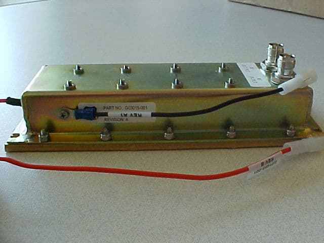
UNION PACIFIC CORPORATION FCC ID: TPBAM090945SF-1H Report # R0510032RF&Exhibits FCC Part 90 Type Approval Report APPENDIX C - EUT PHOTOGRAPHS EUT – Front View EUT – Back View
ID Label/Location Info
UNION PACIFIC CORPORATION FCC ID: TPBAM090945SF-1H Report # R0510032RF&Exhibits FCC Part 90 Type Approval Report APPENDIX A - FCC ID LABELING AND LOCATION Proposed FCC ID Labeling Proposed FCC ID Location Back View of EUT / Proposed Label Location FCC ID: TPBAM090945SF-1H Industry Canada Industrie Canada IC: 6209A-30WUHFPA Model Name: AM090945SF-1H Made by: Union Pacific Corporation
Internal Photos
UNION PACIFIC CORPORATION FCC ID: TPBAM090945SF-1H Report # R0510032RF&Exhibits FCC Part 90 Type Approval Report Chassis – Cover off View EUT – Component View UNION PACIFIC CORPORATION FCC ID: TPBAM090945SF-1H Report # R0510032RF&Exhibits FCC Part 90 Type Approval Report EUT – Solder View EUT – Side View UNION PACIFIC CORPORATION FCC ID: TPBAM090945SF-1H Report # R0510032RF&Exhibits FCC Part 90 Type Approval Report Aluminum Case
Operational Description
Manufacturer PCTEL A/S Product Name 896-960 Radome Antenna Table ASPG931 TESSCO Part No. 411510 1 Image Frequency (MHz) 896-960 Product Narrative Rugged low silhouette transit antenna. Enclosed in a high impact molded ASA radome. Ground plane is required. Includes 4 truss head slotted bolts (#10), 4 self-tapping sheet metal screws and 1 1/8" thick rubber pad. Direct N female termination. Order cable and connectors separately. Gain (dB) Unity Maximum Power (Watts) 100 Whip Length (In.) H 3.4" x L 8" W 3.5" Whip Material Brass rod with ASA plastic radome. Mount Type Surface Cable N/A Connector N/F Advise Customer Warranty 2 Years Qty/Uom 1 EACH Price List $46.50 Gold $23.39 Taken from web page: http://www.tessco.com/products/headerProductSearch.do?searchType=1&searchText=ASPG931&searchField=1
Operational Description
DB586-Y Mirage collinear antenna with horizon blue fiberglass radome. Extremely broad frequency response. Drain plugs at both ends. Product Details for 93743 Manufacturer Andrew Decibel Product Name 890-960 6dB Fiberglass Table DB586-Y TESSCO Part No. 93743 1 Image Specific Freq. (MHz) 890-960 Gain (dBd) 6 Maximum Power Input (Watts) 400 Type Omnidirectional Product Narrative Mirage collinear antenna with horizon blue fiberglass radome. Extremely broad frequency response. Drain plugs at both ends. Bandwidth (MHz) 70 Vert. Beamwidth 18 Deg. Downtilt (deg) None VSWR 1.5:1 Polarization Vertical Gain (dBi) 8.15 Intermodulation N/A Null Fill N/A Sidelobe Suppression (dB) N/A Lightning Prot. DC Ground Size (HxWxD") 4.38' x 1.5" Weight 8.25 Rated Wind Velocity (MPH) 100 Wind Load, (sq ft) 0.328 Lateral Thrust @ RWV (lbs) 14.6 Bending Moment @ RWV (ft lbs) N/A Connector (direct) N Female Jumper Included None Connector Placement Bottom Mount Hdw. Incl. Dual Purpose Mount Incl. Hardware Fits For up to 3" pipe Opt. Pipe Clamp Warranty 1 Year Qty/Uom 1 EACH Price List $604.00 Gold $422.80 Taken from web page: http://www.tessco.com/products/displayProductInfo.do?sku=93743&eventGroup=4&eventPage=1
Operational Description
1) General description. AM090945SF-1H is a general-purpose power amplifier (PA) for Radio transmitter application. It has a built-in, on-off control, which is TTL compatible, and a temperature sensor for over temperature alarm. This manual provides the operating instruction, as well as technical specifications. 2) Operating instruction (User Manual) Figure 1 is the photograph of the PA. All the connections are labeled on the top cover of the PA. The turn-on procedure is described below. A. Connect the PA according to the label shown on the top cover. B. Apply +13.6 volts to the DC pin on the top left corner of PA. C. Apply the radio signal to the amplifier. The radio signal can be from 0.1-watt to 3-watt to reach the desired output power at the “ANT” terminal. D. Monitor the output power at the “ANT” terminal. Figure 1: Photo of AM090945SF-1H PA
Operational Description
3) Technical Manual 3.1) Specification Table 1 shows the specification. The PA delivers a single-tone output power of 30 watts with 9dB gain over the 895-905MHz frequency band. It has a built-in on-off control, which is TTL compatible, and a temperature sensor for over temperature alarm. The PA will work with all possible modulation schemes. Table 1: Module Specifications Parameters Specifications Comments Frequency 895 – 905MHz Gain at 30W > 9dB Gain Variation from 895 to 936 MHz +/- 1dB Power at saturation > 30W Input & Output Impedance 50 Ohms Voltage Supply 13.6V +/- 15% Regulator could be used Supply Current <12A PA ON <0.2A PA OFF T/R Signal TTL Low for TX TTL High for RX Input Impedance > 50k Ohms. For open signal gives TTL High. Module switching time <10ms Temperature Alarm TTL Low for ON TTL High for OFF VSWR Protection Comply Isolator protection RF Connectors TNC-Female DC & Control Interface Feed thru Pins Mechanical Package Size 5.94 x 2.5 x 2.25” 3.2) PA Technical Design AM090945SF-1H is a single-stage power amplifier, which provides amplification from 895MHz to 905MHz with 9dB minimum gain. Figure 2 shows the overall block diagram of the module and Figure 3 shows a photo of the module internal SMT assembly. Figure 2: AM090945SF-1H Module Top Level Schematic Figure 3: Photo of Module SMT Assembly Figures 4, 5, 6, 7 show the detailed schematics of the RF circuit, the +10V Regulator circuit, the T/R Switching circuit and the Temperature Sensing circuit respectively. Figure 4: Detailed Circuit Schematic of RF Circuit (PA) Figure 5: Detailed Circuit Schematic of +10V Regulator Figure 6: Detailed Circuit Schematic of T/R Circuit Figure 7: Detailed Circuit Schematic of Temperature Sensing Circuit
Parts List/Tune Up Info
Table 2. Parts list. DESCRIPTION A) Package HOUSING Lid B) Major Components PCB BOARD Right-Angle TNC Jack 10W LDMOS Power FET 0.9GHz 50W Isolator NPN Switching Transistor NPN Switching Transistor PNP Transistor Temperature Sensor OpAmp 5A Regulator MECHANICAL RELAY C) Resistors Zero Ohms 0603 SMT Resistor 5 Ohms 0603 SMT Resistors 50 Ohms 0603 SMT Resistors 200 Ohms 0603 SMT Resistors 510 Ohms 0603 SMT Resistors 1 kOhm 0603 SMT Resistor 2 kOhms 0603 SMT Resistors 4.7k Ohms 0603 SMT Resistors 5 kOhms 0603 SMT Resistors 7.5 kOhms 0603 SMT Resistors 10 kOhms 0603 SMT Resistors 18 kOhms 0603 SMT Resistors 20k Ohms 0603 SMT Resistors 25k Ohms 0603 SMT Resistors 100 MOhms 0603 SMT Resistors 0.22 Ohm 2512 Thick Film Low Ohm Resitor 1/4W Leaded Resistors Trim Pot 500 Ohms PVZ2 500 Ohms Potentiometer D) Capacitors 100 pF 0603 SMT Capacitor 1000 pF 0603 SMT Capacitor 4.7 pF ATC100 SMT Capacitor 10 pF ATC100 SMT Capacitor 15 pF ATC100 SMT Capacitor 1 pF ATC100 SMT Capacitor 3 pF ATC100 SMT Capacitor 6.8 pF ATC100 SMT Capacitor 10 pF ATC100 SMT Capacitor 0.1 uF 0805 Capacitor 1 uF 35V Capacitor 3 - 10pF Variable Capacitor E) Misc. 5000pF 10A DC Pin Low Current DC Pins with filter 4-40 Ground Lug 2-56 1/4" Socket Screws for PCB 4-40 1/4" Socket Screws for Isolator Assembly Teflon Barrel No. 2 Lock washer No. 4 Lock washer Jumpers
Parts List/Tune Up Info
3.3) Tuning & Adjustments Procedure No user tuning is required during module installation. The following tuning procedures are used by factory personnel during module manufacturing. a) +10V Regulator Output Adjustment Make sure the regulator output is +10V ± 0.2V. If the output needs adjustment use the variable resistor labeled R bias in Figure 5 to adjust the output voltage. Change supply voltage of +13.6V by ± 2.0V and make sure regulator output is stable around +10V (i.e. < 0.3V variation). b) T/R Control Check Make sure the SMT switch is in TX mode for T/R Signal < 0.5V and in RX mode for > 2.2V. No adjustment is needed for the T/R circuit in Figure 6. Measure input resistance of T/R pin, value should be >50kOhms. Disconnect T/R signal module should revert to RX mode. Total module current should drop below 0.1A in RX mode. c) Quiescent PA Current Adjustment With module turned on in TX mode adjust the variable resistor labeled Gate Bias Adjust in Figure 6 until V gs =+1.8V. Measure the module DC current under no RF input and in the TX mode. Adjust Gate Bias incrementally until total module quiescent current is equal to 2A. Note that under RF power the current increases, therefore this adjustment should be made with no RF input power. d) Temperature Sensing Adjustment Place Module on a hot plate and adjust the hot plate temperature to 80°C. With the module turned on in TX mode increase the hot plate temperature gradually to 90°C. The Temperature Alarm show go from TTL high to TTL low. Adjust RT resistor in Figure 7 to change the threshold temperature to be at +85°C ± 4°C. e) RF Module TX Gain Connect the module to the Network analyzer. Turn on module and apply low T/R signal for TX mode and measure gain using S-parameter setup gain should be >10dB from 890 – 910MHz. If gain needs adjustment change values of R s & R p resistors in Figure 4. Gain at 940MHz should be < gain at 910MHz. f) RF Module Input Return Loss Input return loss of module should be > 10dB from 890 to 910MHz. Input return loss could be adjusted used tunable capacitor labeled CT in Figure 4. Output return loss should be >15dB. g) RF Module RX Gain Connect the module to the Network analyzer. Turn on module and apply high T/R signal for RX mode and measure gain using S-parameter setup insertion loss should be < 1dB from 890 – 910MHz. Input & output return losses should be > 15dB. h) RF Module Power Using AMCOM power setup, connect then turn on the module in TX mode. Adjust signal generator frequency to 900MHz and increase input power until output power is equal to 30W (i.e. 34.8dBm). RF Gain of Module should not drop below 9dB at 30W output power. Power could be adjusted using the quiescent DC current of the PA by adjusting V gs . The DC current should be increased in increments of 100mA and repeat power measurements until desired power is achieved. Sweep power from 890 to 910MHz to make sure power and gain are flat with frequency. Appendix I shows the Module Test Traveler used in manufacturing. Appendix I Test Traveler of 30W T/R Module (P/N AM090945SF-1H) Part Serial No.: Date: A) TX State (Voltage Supply= 13.6V ± 15%) Parameter Specification Measured Pass /Fail Comment Frequency 895 – 905MHz Small Signal Gain - 13.6dB Gain at 30W output > 8dB 11.1dB Power at Saturation > 30W 46W Gain > 8dB Input Return Loss > 10dB 17.6dB Output Return Loss > 10dB 23.3dB Supply Current < 12A 8.4A T/R Signal Threshold for TX > 0.5V 0.7V Temp. Alarm ON < 0.5V 0.22V Bottom housing at > 88°C Temp. Alarm OFF > 2.2V 4.6V Bottom housing at < 82°C Module switching time < 10ms 6ms VSWR Stability Stable Stable VSWR < 5 B) RX State (Voltage Supply= 13.6V ± 15%) Parameter Specification Measured Pass /Fail Comment Frequency 895 – 905MHz Insertion Loss for RX < 0.7dB 0.55dB Input Return Loss > 15dB 24dB Output Return Loss > 15dB 20dB Supply Current < 0.2A 0.02A T/R Signal Threshold for RX > 2.2V 1.5V Module switching time < 10ms 6ms Test Technician: ________________________________ Signature: _______________ Quality Control: ________________________________ Signature: _______________
RF Exposure Info
§1.1310 and §2.1091 - RF EXPOSURE According to §1.1307, systems operating under the provisions of this section shall be operated in a manner that ensures that the public is not exposed to radio frequency energy level in excess of the Commission’s guidelines. According to §1.1310 and §2.1091 RF exposure is calculated. Limits for Maximum Permissive Exposure (MPE) Frequency Range (MHz) Electric Field Strength (V/m) Magnetic Field Strength (A/m) Power Density (mW/cm 2 ) Averaging Time (minute) Limits for Occupational Population/Controlled Exposure 0.3-1.34 614 1.63 *(100) 30 1.34-30 824/f 2.19/f *(180/f\2\) 30 30-300 27.5 0.073 0.2 30 300-1500 / / f/1500 30 1500-100,000 / / 1.0 30 f = frequency in MHz * = Plane-wave equivalent power density MPE Prediction Predication of MPE limit at a given distance Equation from page 18 of OET Bulletin 65, Edition 97-01 S = PG/4πR² Where: S = power density P = power input to antenna G = power gain of the antenna in the direction of interest relative to an isotropic radiator R = distance to the center of radiation of the antenna Uplink: Transmitted with Andrew Decibel Antenna: Maximum peak output power at antenna input terminal: 44.9 (dBm ) Maximum peak output power at antenna input terminal: 30903 (mW) Prediction distance: 164 (cm) Predication frequency: 900 (MHz) Antenna Gain (typical): 8.15 (dBi) antenna gain: 6.53 (numeric) Power density at predication frequency at 164 cm: 0.597 (mW/cm 2 ) MPE limit for uncontrolled exposure at prediction frequency: 0.6 (mW/cm 2 ) UNION PACIFIC CORPORATION FCC ID: TPBAM090945SF-1H Report # R0510032RF&Exhibits FCC Part 90 Type Approval Report Transmitted with 896-960 Radome Antenna: Maximum peak output power at antenna input terminal: 44.9 (dBm) Maximum peak output power at antenna input terminal: 30903 (mW) Prediction distance: 65 (cm) Predication frequency: 900 (MHz) Antenna Gain (typical): 0 (dBi) antenna gain: 1 (numeric) Power density at predication frequency at 65 cm: 0.582 (mW/cm 2 ) MPE limit for uncontrolled exposure at prediction frequency: 0.6 (mW/cm 2 ) Downlink: Transmitted with Andrew Decibel Antenna: Maximum peak output power at antenna input terminal: 44.2 (dBm ) Maximum peak output power at antenna input terminal: 26303 (mW) Prediction distance: 151 (cm) Predication frequency: 935 (MHz) Antenna Gain (typical): 8.15 (dBi) antenna gain: 6.53 (numeric) Power density at predication frequency at 151 cm: 0.599 (mW/cm 2 ) MPE limit for uncontrolled exposure at prediction frequency: 0.57 (mW/cm 2 ) Transmitted with 896-960 Radome Antenna: Maximum peak output power at antenna input terminal: 44.2 (dBm ) Maximum peak output power at antenna input terminal: 26303 (mW) Prediction distance: 60 (cm) Predication frequency: 935 (MHz) Antenna Gain (typical): 0 (dBi) antenna gain: 1 (numeric) Power density at predication frequency at 60 cm: 0.58 (mW/cm 2 ) MPE limit for uncontrolled exposure at prediction frequency: 0.57 (mW/cm 2 ) Test Result For Uplink, when transmitted with Andrew Decibel Antenna, the predicted distance is 164cm. when transmitted with 896-960 Radome Antenna, the predicted distance is 65cm. For Downlink, when transmitted with Andrew Decibel Antenna, the predicted distance is 151cm. when transmitted with 896-960 Radome Antenna, the predicted distance is 60cm.
Schematics
Figures 4, 5, 6, 7 show the detailed schematics of the RF circuit, the +10V Regulator circuit, the T/R Switching circuit and the Temperature Sensing circuit respectively. Figure 4: Detailed Circuit Schematic of RF Circuit (PA) Figure 5: Detailed Circuit Schematic of +10V Regulator Figure 6: Detailed Circuit Schematic of T/R Circuit Figure 7: Detailed Circuit Schematic of Temperature Sensing Circuit
Test Report
Note: The test report is specially limited to the above company and this particular sample only. It may not be duplicated without prior written consent of Bay Area Compliance Laboratory Corporation. This report must not be used by the client to claim product certification, approval, or endorsement by NVLAP, NIST or any agency of the US Government. FCC PART 90 TYPE APPROVAL EMI MEASUREMENT AND TEST REPORT For UNION PACIFIC CORPORATION 1400 Douglas Street, Omaha, NE 68179, USA FCC ID: TPBAM090945SF-1H This Report Concerns: Original Report Equipment Type: Booster Amplifier for Portable Transceiver Test Engineer: James Ma Report No.: R0510032 Report Date: 2005-11-14 Reviewed By: Daniel Deng Prepared By: Bay Area Compliance Laboratory Corporation 230 Commercial Street Sunnyvale, CA 94085 Tel: (408) 732-9162 Fax: (408) 732 9164 UNION PACIFIC CORPORATION FCC ID: TPBAM090945SF-1H Report # R0510032Rpt Page 2 of 23 FCC Part 90 Type Approval Report TABLE OF CONTENTS GENERAL INFORMATION.......................................................................................................................................3 PRODUCT DESCRIPTION FOR EQUIPMENT UNDER TEST (EUT) ....................................................................................3 OBJECTIVE...................................................................................................................................................................3 RELATED SUBMITTAL(S)/GRANT(S).............................................................................................................................3 TEST METHODOLOGY..................................................................................................................................................3 TEST FACILITY.............................................................................................................................................................3 SYSTEM TEST CONFIGURATION ..........................................................................................................................4 JUSTIFICATION.............................................................................................................................................................4 BLOCK DIAGRAM.........................................................................................................................................................4 EQUIPMENT MODIFICATIONS.......................................................................................................................................4 POWER SUPPLY INFORMATION.....................................................................................................................................4 LOCAL SUPPORT EQUIPMENT.......................................................................................................................................4 INTERFACE PORTS AND CABLE IN................................................................................................................................4 TEST SETUP BLOCK DIAGRAM.....................................................................................................................................5 SUMMARY OF TEST RESULTS ...............................................................................................................................6 §2.1046, AND §90.205 - RF OUTPUT POWER .........................................................................................................7 PROVISION APPLICABLE...............................................................................................................................................7 TEST PROCEDURE........................................................................................................................................................7 TEST EQUIPMENT.........................................................................................................................................................7 ENVIRONMENTAL CONDITIONS....................................................................................................................................7 TEST RESULTS.............................................................................................................................................................8 §2.1049, § 90.209, § 90.210 – OCCUPIED BANDWIDTH .........................................................................................9 APPLICABLE STANDARD..............................................................................................................................................9 TEST PROCEDURE........................................................................................................................................................9 TEST EQUIPMENT.........................................................................................................................................................9 ENVIRONMENTAL CONDITIONS....................................................................................................................................9 TEST RESULTS.............................................................................................................................................................9 §2.1051 AND §90.210 - SPURIOUS EMISSIONS AT ANTENNA TERMINALS ................................................16 APPLICABLE STANDARD............................................................................................................................................16 TEST PROCEDURE......................................................................................................................................................16 TEST EQUIPMENT.......................................................................................................................................................16 ENVIRONMENTAL CONDITIONS....................................................…
Text truncated - open the document above for the full version.
Test Setup Photos
UNION PACIFIC CORPORATION FCC ID: TPBAM090945SF-1H Report # R0510032RF&Exhibits FCC Part 90 Type Approval Report APPENDIX B - TEST SETUP PHOTOGRAPHS Uplink Radiated Emission With Andrew Vertical Antenna - Front View Uplink Radiated Emission With Andrew Vertical Antenna - Rear View UNION PACIFIC CORPORATION FCC ID: TPBAM090945SF-1H Report # R0510032RF&Exhibits FCC Part 90 Type Approval Report Downlink Radiated Emission With Andrew Vertical Antenna - Front View Downlink Radiated Emission With Andrew Vertical Antenna - Rear View UNION PACIFIC CORPORATION FCC ID: TPBAM090945SF-1H Report # R0510032RF&Exhibits FCC Part 90 Type Approval Report Uplink Radiated Emission With AS Antenna - Front View Uplink Radiated Emission With AS Antenna - Rear View UNION PACIFIC CORPORATION FCC ID: TPBAM090945SF-1H Report # R0510032RF&Exhibits FCC Part 90 Type Approval Report Downlink Radiated Emission With AS Antenna - Front View Downlink Radiated Emission With AS Antenna - Rear View
Contact Information
Applicant
Dan Rubin(General Director)
Test Firm
Bay Area Compliance LaboratoryJohn Chan
Technical Specifications
| # | Rule Parts | Frequency Range | Power Output | Emission |
|---|---|---|---|---|
| 2 | 9 | 935.8875 MHz - 936.9875 MHz | 35 W | G7W |
Other Applications from Union Pacific Corporation
TPBMCA8030
Sep 19, 2008MCA8030 Booster Amplifier
Equipment Class
AMP - Amplifier