U6SJW-1909MSmart wake up light
Shenzhen J.W. Industries Co., Ltd.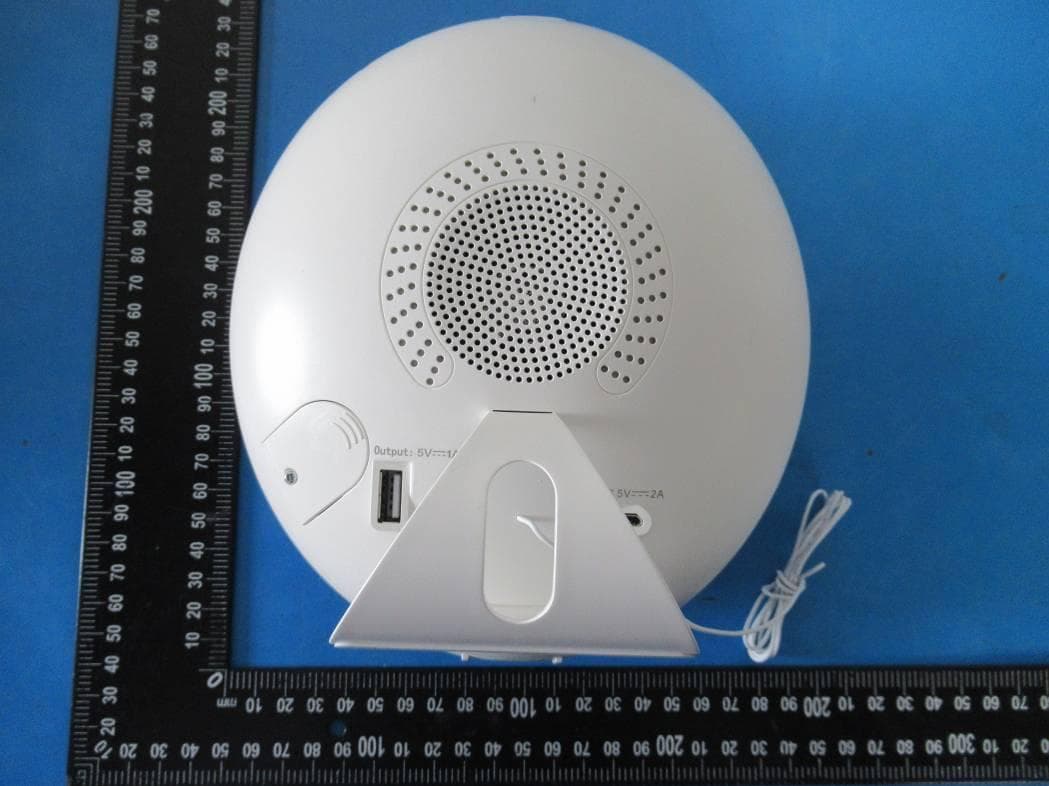
Click to zoom
Application Details
- Equipment Class
- DTS - Digital Transmission System
- Date of Grant
- May 31, 2020
- Application Purpose
- Original Equipment
- Date of Application
- May 31, 2020
- Equipment Note
- Smart wake up light
- Frequency Range
- 2412.00000000 - 2462.00000000
- Country
- China
Documents & Files
Document Text
Text extracted from the exhibit documents filed with the FCC. Open a document above to read the original.
Users Manual
Smart wake up light This equipment has been tested and found to comply with the limits for a Class B digital device, pursuant to part 15 of the FCC Rules. These limits are designed to provide reasonable protection against harmful interference in a residential installation. This equipment generates, uses and can radiate radio frequency energy and, if not installed and used in accordance with the instructions, may cause harmful interference to radio communications. However, there is no guarantee that interference will not occur in a particular installation. If this equipment does cause harmful interference to radio or television reception, which can be determined by turning the equipment off and on, the user is encouraged to try to correct the interference by one or more of the following measures: • Reorient or relocate the receiving antenna. • Increase the separation between the equipment and receiver. • Connect the equipment into an outlet on a circuit different from that to which the receiver is connected. • Consult the dealer or an experienced radio/TV technician for help. Caution: Any changes or modifications to this device not explicitly approved by manufacturer could void your authority to operate this equipment. This device complies with part 15 of the FCC Rules. Operation is subject to the following two conditions: (1) This device may not cause harmful interference, and (2) this device must accept any interference received, including interference that may cause undesired operation. The device has been evaluated to meet general RF exposure requirement. The device can be used in portable exposure condition without restriction.
Cover Letter(s)
Date: 2020.05.27 Equipment Autorisation Division Federal Communications Commission 7435 Oakland Mills Road Columbia, MD 21046 FCC ID: U6SJW-1909M Product Name: Smart wake up light Request for Confidentiality Pursuant to Sections 0.457 and 0.459 of the commissions rules, we hereby request that the following documents be held confidential: Schematics Long-term confidential Block diagram Long-term confidential Operation description Long-term confidential These materials contain trade secrets and proprietary information and are not customarily released to the public. The public disclosure of this information might be harmful to the company and provide unjustified benefits to our competitors. Signature: 2020.05.27 Signatory Name Mary Ma Position Sales Company Name Shenzhen J.W. Industries Co., Ltd. Address 4/F, Block C6, Hengfeng Industrial Area, Xi’xiang Town, Bao’an District, Shenzhen, Guangdong, China Tel 0755-27865528 Fax / Email [email protected] Shenzhen J.W. Industries Co., Ltd.
External Photos
FCC ID: U6SJW-1909M
ID Label/Location Info
1.5cm 0.6cm Label Location FCC ID: U6SJW-1909M Shenzhen J.W. Industries Co., Ltd. Model name: Wake up light speaker Model No.: JW-1909M
Internal Photos
FCC ID: U6SJW-1909M ANT
RF Exposure Info
RF Exposure evaluation According to 447498 D01 General RF Exposure Guidance v06 The 1-g and 10-g SAR test exclusion thresholds for 100 MHz to 6 GHz at test separation distances ≤ 50 mm are determined by: [(max. power of channel, including tune-up tolerance, mW)/(min. test separation distance, mm)] ·[√f(GHz)] ≤ 3.0 for 1-g SAR and ≤ 7.5 for 10-g extremity SAR, where f(GHz) is the RF channel transmit frequency in GHz Power and distance are rounded to the nearest mW and mm before calculation The result is rounded to one decimal place for comparison MPE Ratios for 2.4GHz WLAN Mode f (GHz) Antenna Distance (mm) RF output power SAR Test Exclusion Threshold SAR Test Exclusion dBm mW 2.4G WLAN 2.462 5 8.37 6.87 2.16 < 3.0 Yes Then SAR evaluation is not required
Test Report
FCC TEST REPORT FCC ID: U6SJW-1909M On Behalf of Shenzhen J.W. Industries Co., Ltd. Smart wake up light Model No.: JW-1909M Prepared for : Shenzhen J.W. Industries Co., Ltd. Address : 4/F, Block C6, Hengfeng Industrial Area, Xi’xiang Town, Bao’an District, Shenzhen, Guangdong, China Prepared By : Shenzhen Alpha Product Testing Co., Ltd. Address : Building i, No.2, Lixin Road, Fuyong Street, Bao’an District, 518103, Shenzhen, Guangdong, China Report Number : A2004234-C01-R06 Date of Receipt : April 28, 2020 Date of Test : May 14-21, 2020 Date of Report : May 26, 2020 Version Number : V0 Page 2 of 61 Report No.: A2004234-C01-R06 TABLE OF CONTENTS Description Page 1. Summary of Standards And Results ------------------------------------------------------------------- 6 1.1. Description of Standards and Results ------------------------------------------------------------ 6 2. General Information -------------------------------------------------------------------------------------- 7 2.1. Description of Device (EUT) ---------------------------------------------------------------------- 7 2.2. Accessories of Device (EUT) --------------------------------------------------------------------- 8 2.3. Tested Supporting System Details ---------------------------------------------------------------- 8 2.4. Block Diagram of connection between EUT and simulators --------------------------------- 8 2.5. Test Mode Description ----------------------------------------------------------------------------- 9 2.6. Test Conditions ------------------------------------------------------------------------------------ 10 2.7. Test Facility ---------------------------------------------------------------------------------------- 10 2.8. Measurement Uncertainty ----------------------------------------------------------------------- 11 2.9. Test Equipment List ------------------------------------------------------------------------------ 12 3. Spurious Emission --------------------------------------------------------------------------------------- 13 3.1. Test Limits ----------------------------------------------------------------------------------------- 13 3.2. Test Procedure ------------------------------------------------------------------------------------- 13 3.3. Test Setup ------------------------------------------------------------------------------------------ 14 3.4. Test Results ---------------------------------------------------------------------------------------- 15 4. Power line Conducted Emission ---------------------------------------------------------------------- 20 4.1. Test Limits ----------------------------------------------------------------------------------------- 20 4.2. Test Procedure ------------------------------------------------------------------------------------- 20 4.3. Test Setup ------------------------------------------------------------------------------------------ 20 4.4. Test Results ---------------------------------------------------------------------------------------- 21 5. Conducted Maximum Output Power --------------------------------------------------------------- 22 5.1. Test limits ------------------------------------------------------------------------------------------ 22 5.2. Test Procedure ------------------------------------------------------------------------------------- 22 5.3. Test Setup ------------------------------------------------------------------------------------------ 22 5.4. Test Results ---------------------------------------------------------------------------------------- 22 6. Power Spectral Density --------------------------------------------------------------------------------- 24 6.1. Test limits ------------------------------------------------------------------------------------------ 24 6.2. Test Procedure ------------------------------------------------------------------------------------- 24 6.3. Test Setup ------------------------------------------------------------------------------------------ 24 6.4. Test Results ---------------------------------------------------------------------------------------- 25 7. Bandwidth ------------------------------------------------------------------------------------------------- 30 7.1. Test limits ------------------------------------------------------------------------------------------ 30 7.2. Test Procedure ------------------------------------------------------------------------------------- 30 7.3. Test Setup ------------------------------------------------------------------------------------------ 30 7.4. Test Results ---------------------------------------------------------------------------------------- 30 8. Band Edge Check ---------------------------------------------------------------------------------------- 40 8.1. Test limits ------------------------------------------------------------------------------------------ 40 8.2. Test Procedure ------------------------------------------------------------------------------------- 40 8.3. Test Setup ------------------------------------------------------------------------------------------ 40 8.4. Test Results ---------------------------------------------------------------------------------------- 40 9. Antenna Requirement ---------------------------------------------------------------------------------- 47 Page 3 of 61 Report No.: A2004234-C01-R06 9.1. Standard Requirement ---------------------------------------------------------------------------- 47 9.2. Antenna Connected Construction --------------------------------------------------------------- 47 9.3. Results ---------------------------------------------------------------------------------------------- 47 10. Test setup photo ------------------------------------------------------------------------------------------ 48 10.1. Photos of Radiated emission -------------------------------------------------------------------- 48 10.2. Photos of Conducted Emission test -------------------------------…
Text truncated - open the document above for the full version.
Test Setup Photos
FCC ID: U6SJW-1909M 1.1. Photos of Radiated emission 1.2. Photos of Conducted Emission test
Contact Information
Applicant
Mary Ma(Manager of Marketing Dept.)
Test Firm
Shenzhen Alpha Product Testing Co., LTD.Simple Guan
[email protected]+86 755 29766001-810
Technical Specifications
| # | Rule Parts | Frequency Range | Power Output |
|---|---|---|---|
| 1 | 15C | 2.41 GHz - 2.46 GHz | 6.87 mW |
Other Applications from Shenzhen J.W. Industries Co., Ltd.
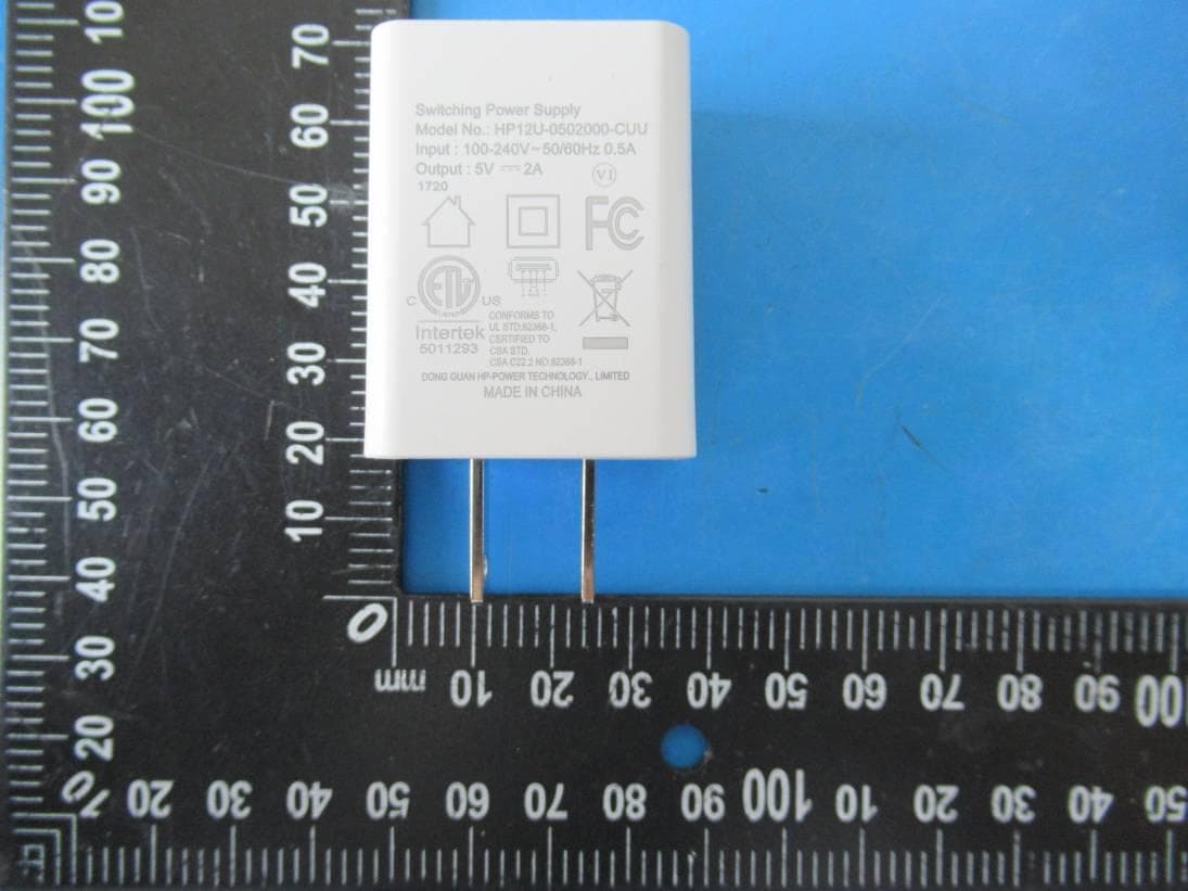
U6SJW-1909N
Jun 01, 2020Wake up light speaker
Equipment Class
DSS - Part 15 Spread Spectrum Transmitter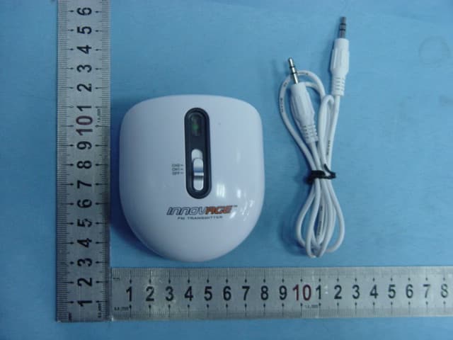
U6SJW1575
Apr 10, 2007FM Transmitter
Equipment Class
DXX - Part 15 Low Power Communication Device Transmitter