W2STLG10UA03HED WIRELESS-GS UART ADAPTER
CEC Huada Electronic Design Co., Ltd.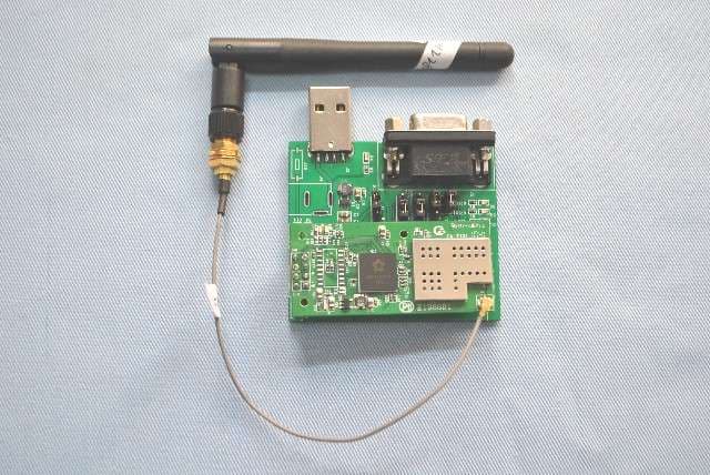
Click to zoom
Application Details
- Equipment Class
- DTS - Digital Transmission System
- Date of Grant
- Jan 25, 2011
- Application Purpose
- Original Equipment
- Date of Application
- Jan 25, 2011
- Equipment Note
- HED WIRELESS-GS UART ADAPTER
- Frequency Range
- 2412.00000000 - 2462.00000000
- Country
- China
Documents & Files
Document Text
Text extracted from the exhibit documents filed with the FCC. Open a document above to read the original.
Users Manual
Characteristic Interface 2*4 pins of Interface: HDR254M-2X4 The range of baud rate: 1200~ 115200bps RTS / CTS Hardware flow control single 3.3V power supply Wireless support IEEE802.11b/g wireless standards support the range of frequency: 2.412~2.484 GHz support two types of wireless networks: Ad hoc and Infrastructure support multiple security authenti- cation mechanisms: WEP64/WEP128/ TKIP/CCMP(AES) WEP/WPA-PSK/WPA2-PSK support quick networking support wireless roam Others support multiple network protocols: TCP/UDP/ICMP/DHCP/DNS/HTT P support two types of work modes: auto and command Support transparent transmission mode support AT+ instruction set summarize TLG10UA03 is the new third-generation embedded Uart-Wifi modules studied by CEC Huada Electronic Design Co., Ltd. Uart-Wif is an embedded module based on the Uart serial,according with the WiFi wireless WLAN standards, It accords with IEEE802.11 protocol stack and TCP / IP protocol stack,and it enables the data conversion between the user serial and the wireless network module. through the Uart-Wifi module, the traditional serial devices can easily access to the wireless network. TLG10UA03 does a comprehensive hardware and software upgrades based on the products of the first two generations,now it’s more functional and more Convenient to use,its main features include, Support transparent transmission of serial completely,and achieve a plug and play serial. Support new AT+instruction set, Which is all based on ASCII format, it’s simple to use and pellucid. Support more perfect TCP/IP protocol tack, support DHCP protocol for dynamicassignation of IP address and DNS domain name parsing. Embed WEB server, and achieve the long-range parameters configur -ation through wireless network with IE browser. Support more prefect transmission performance,the maximum sending rate can reach to 11KB/s. support a variety of parameters configuration methods: serial/WEB server/wireless conn- ection Application intelligent bus network, such as wireless credit card machine small financial payment network, such as wireless POS machine industrial equipment networking, such as wireless sensor things Contents 1 INTRODUCTION ............................................................................................................................................ 6 2 OVERVIEW ................................................................................................................... 错误!未定义书签。 2.1 TECHNICAL SPECIFICATION ........................................................................................ 错误!未定义书签。 2.2 HARDWARE INTRODUCTION........................................................................................ 错误!未定义书签。 2.2.1 Mechanical Dimension ..................................................................................... 错误!未定义书签。 2.2.2 External Interface .............................................................................................. 错误!未定义书签。 2.2.3 Antenna(optional) ........................................................................................ 错误!未定义书签。 2.2.4 Serial Adapter (optional) ................................................................................... 错误!未定义书签。 2.2.5 Wireless adapter(optional) ........................................................................... 错误!未定义书签。 2.3 MAIN FEATURES ......................................................................................................... 错误!未定义书签。 2.3.1 Wireless Network Connection .......................................................................... 错误!未定义书签。 2.3.2 Plug and Play Serial .......................................................................................... 错误!未定义书签。 2.3.3 Command Mode of Serial ................................................................................. 错误!未定义书签。 2.3.4 TCP/IP Protocol stack ....................................................................................... 错误!未定义书签。 2.3.5 Flexible Parameter Configuration ..................................................................... 错误!未定义书签。 2.3.6 Multi-functional GPIO ...................................................................................... 错误!未定义书签。 2.3.7 Firmware upgrade online .................................................................................. 错误!未定义书签。 3 QUICK START WIZARD ................................................................................................................................ 8 3.1 PREPARATION ............................................................................................................................................... 8 3.2 SETTING PARAMETERS .................................................................................................................................. 8 3.3 TESTING...................................................................................................................................................... 10 4 PRODUCT DESIGN GUIDE......................................................................................... 错误!未定义书签。 4.1 HARDWARE CONNECTION .......................................................................................... 错误!未定义书签。 4.2 WORK MODE ............................................................................................................... 错误!未定义书签。 4.2.1 Start-up mode selection ..................................................................................... 错误!未定义书签。 4.2.2 Auto-work mode ............................................................................................... 错误!未定义书签。 4.2.3 Command work mode ....................................................................................... 错误!未定义书签。 4.3 PARAMETER DETAILS ................................................................................................. 错误!未定义书签。 4.3.1 Wireless parameters ..............................................................…
Text truncated - open the document above for the full version.
Attestation Statements
CEC Huada Electronic Design Co.,Ltd. Floor 5、6,Building A,Wangjing Science and Technology Park,No.2.,Lizezhonger Rd.Chaoyang District Beijing,100102,P.R.China Federal Communications Commission Authorization and Evaluation Division 1435 Oakland Mills Road Columbia, MD 21046 Date: January 17, 2011 Subject: FCC Application for FCC ID: W2STLG10UA03 To Whom It May Concern: We, the undersigned, hereby attest to the fact that we will apply the declaration of Conformity procedure to the class B computer peripheral portion of this composite filing. Sincerely, Ms.Gao Ning/ Engineer
Block Diagram
Flash 44M OSC LED RF ALL2230S 4*2 pin plug with 2.54 mm pin space 3.3V/2.8V LDO 3.3V Balun Switch HED05W01SA IPX 3.3/1.8 DCDC
Cover Letter(s)
CEC Huada Electronic Design Co.,Ltd. Floor 5、6,Building A,Wangjing Science and Technology Park,No.2.,Lizezhonger Rd.Chaoyang District Beijing,100102,P.R.China Date: January 17, 2011 Subject: FCC Application for FCC ID: W2STLG10UA03 To Whom It May Concern: There’s a EUT-Sample that would like to have your authorization as a modular approval. The specific product as below, Wireless Module with its designed features and specified description, meets special requirements for full modular approval on FCC Part 15.212 by cross-refrence list below. Company: CEC Huada Electronic Design Co.,Ltd. Product Name: HED Wireless-GS UART Adapter Antenna: Dipole Unique Antenna Connector: UFL Model Number: TLG10UA03 FCC ID: W2STLG10UA03 Requirement of FCC Part 15.212 Reference to TLG10UA03 1. The radio elements of the modular transmitter must have their own shielding. The module has its own RF shielding. Please see external photo.pdf 2. The modular transmitter must have buffered modulation/data inputs. The modular has buffered data inputs, it is integrated in chip Wireless Module. Please see block diagram.pdf 3. The modular transmitter must have its own power supply regulation The modular transmitter has its own power supply regulation built in TLG10UA03. Please see schematics.pdf 4. The modular transmitter must comply with the antenna and transmission system requirements of Section 15.203, 15.204 (b) and 15.204 (c). The TLG10UA03 meets the FCC antenna requirements. It has a unique connector(UFL Connector). Please see external photo.pdf 5. The modular transmitter must be tested in a stand-alone configuration, i.e., the module must not be inside another device during testing. The TLG10UA03 was tested with host device. Please refer to test report in details. 6. The modular transmitter must be equipped with either a permanently affixed label or must be capable of electronically displaying its FCC identification number. The label position of TLG10UA03 is clearly indicated. Please see the label.pdf 7. The modular transmitter must comply with any specific rules or operating requirements that ordinarily apply to a complete transmitter and the manufacturer must provide adequate instructions along with the module to explain any such requirements. A copy of these instructions must be included in the application for equipment authorization. The TLG10UA03 is compliant with all applicable FCC rules. Detail instructions are given in the Users Manual. Please see user manual.pdf 8. The modular transmitter must comply with any applicable RF exposure requirements in its final configuration. The TLG10UA03 comply with applicable RF exposure requirements. Please see test report. pdf Sincerely, Ms.Gao Ning/ Engineer
External Photos
Main & RF board component side Assistant Tools
ID Label/Location Info
This device complies with Part 15 of the FCC Rules. Operation is subject to the following two conditions: (1) this device may not cause harmful interference, and (2) this device must accept any interference received, including interference that may cause undesired operation. The Label must not be a stick-on paper label. The Label on these products must be permanently affixed to the product and readily visible at the time of purchase and must last the expected lifetime of the equipment not be readily detachable. Proposed Label Location on EUT EUT Bottom View/Proposed FCC ID Label Location FCC ID: W2STLG10UA03
Internal Photos
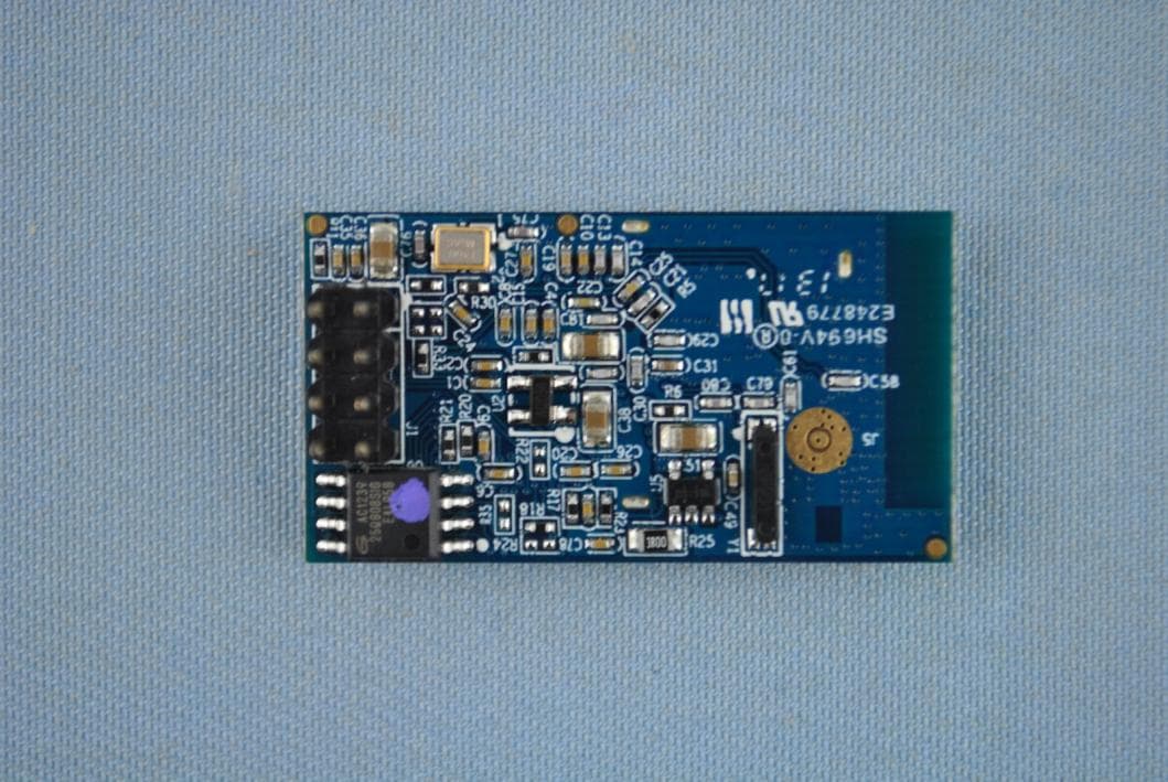
Main & RF board solder side
Operational Description
1 北京中电华大电子设计有限责任公司 CEC Huada Electronic Design Co., Ltd. 4*2 pin plug with 2.54mm pin space: used to connect wireless LAN module and the UART interface of the system to establish data communication and 3.3V Power Supply. LDO、DC/DC: Power supply for wireless LAN module with Input 3.3V and Output 1.8V or 2.8V. STAU Chip (HED05W01SA):This is in line with the GB15629 a series of national wireless standards, in line with China's safety standards for wireless local area network (WAPI)and IEEE802.11a/b/g related to the safety standards of multimode wireless base-band / MAC chip. Frequency : 44MHz. RF Chip (AL2230S):Modulation/demodulation 2.4GHz RF signal. Frequency: 2.4GHz. Flash: Storage of Firmware. CLOCK: Supply 44M clock signal for STAU and RF. Balun: Balance to unbalance. Switch: It is an IC FET SPDT switch in a low-cost miniature SC-70 6-lead plastic package. The features low insertion loss and positive voltage operation with very low DC power consumption. This general-purpose switch can be used in a variety of telecommunications applications. IPX (Antenna): connect to Antenna .
Schematics
55 44 33 22 11 D D C C B B A A GC0 RF1RF16RF17PA_24G_EN RF4RF7 VCC_2V8 RXON PADET RF12 TXON RF_CTL_REG1 TXQN TXQP TXIN TXIP TXON VCC_2V8 RF13 AL36 RF15RF14 RXON RF5 RF6 VDD33 RXIN FREF RXIP VCC_2V8 VCC_2V8 RF_SENRF_SCLKRF_SDATA RF2 AL32 AL38 RXHP RXQN RXQP VCC_2V8 GC1GC2GC3GC4GC5GC6 VCC_2V8 VCC_2V8 VCC_2V8 VCC_2V8 VCC_2V8 VDD33 VDD33 VDD33 VCC_2V8 VCC_2V8 VCC_2V8 RXON FREFRF_SENRF_SCLK RXHP RF_SDATA PA_24G_EN RF_CTL_REG1 TXQN TXQP TXIN TXIP GC1GC2 TXON GC3GC4GC5 RXQN GC6 RXQP RXIN GC0 RXIP C8010pFC8010pF C61100nFC61100nF L15 1.1nHL15 1.1nH R36 5.6K R36 5.6K C772.2pFC772.2pF L14 1.1nHL14 1.1nH U11 BL2012 U11 BL2012 UMBA 1 GND 2 BA-1 3 BA-2 4 GND2 5 NC 6 U12 AL2230S U12 AL2230S GC2 1 GC3 2 GC4 3 GC5 4 RFIN 5 VCCFE-V28 6 GC6 7 GC7 8 RFOUT_N 9 RFOUT_P 10 VCCPA3_V33 11 PAON 12 VCCPA2_V33 13 VCCPA1_V33 14 PDOUT 15 VCCPD_V28 16 TXON 17 TX_IP 18 TX_IN 19 TX_QP 20 TX_QN 21 VREF12 22 PLLON 23 TPOUT 24 FREF 25 LE 26 CLK 27 DATA 28 VCCDIG_V28 29 VCCPLL_V28 30 VCCP_V28 31 CP 32 VCCDIV_V28 33 VTUNE_NC 34 GNDVCO 35 REG_V24 36 VCCREG_V28 37 RBIAS 38 RXHP 39 RSSIOUT 40 RX_QN 41 RX_QP 42 RX_IN 43 RX_IP 44 VCCZIF_V28 45 VCCMIX_V28 46 RXON 47 GC1 48 GND 49 C888.2pFC888.2pF C89 NCC89 NC L13NCL13NC C1010.5pFC1010.5pF C991.8pFC991.8pF L18 2nHL18 2nH C914.7pFC914.7pF C62100nFC62100nF C75 2.2pFC75 2.2pF C1030.5pFC1030.5pF C66 1nF C66 1nF C63100nFC63100nF U9 HWS408 U9 HWS408 RX 1 GND 2 TX 3 RXEN 4 ANT 5 RXEN 6 C95 1.5pF C95 1.5pF C5710uFC5710uF J2 TC35 J2 TC35 RF 1 GND 2 GND2 3 GND3 4 C78 8.2pFC78 8.2pF C1020.5pFC1020.5pF C762.2pFC762.2pF C838.2pFC838.2pF C87 8.2pF C87 8.2pF C5810uFC5810uF C96 1.5pF C96 1.5pF C1001.2pFC1001.2pF C943.3pFC943.3pF R3512KR3512K C9722nFC9722nF C924.7pFC924.7pF C98 3.3nFC98 3.3nF C60 100nFC60 100nF C93 NC C93 NC 55 44 33 22 11 D D C C B B A A VDD18 U7_4 NPORESET U2_3 U2_4 XIN FREF U6_5 VCC_2V8 VDD33 VDD33 VDD33 VDD33 VDD18 VCC_2V8 VDD33 VCC_2V8 FREF XIN NPORESET C6410pFC6410pF C221uFC221uF C730.01uFC730.01uF C10410uFC10410uF C5610uFC5610uF C651nFC651nF C5110uFC5110uF C740.1uFC740.1uF L103.3uHL103.3uH R28 12K R28 12K U7 RP1202-28V U7 RP1202-28V VIN 1 GND 2 EN 3 BP 4 VOUT 5 R27200R27200 C5410uFC5410uF U2OSCU2OSC E/D 1 GND 2 OUT 3 VCC 4 U6 RT8009 U6 RT8009 VIN 1 GND 2 EN 3 FB/VOUT 4 LX 5 R2065R2065 C55 10uF C55 10uF C590.1uFC590.1uF C290.1uFC290.1uF C6810uFC6810uF 55 44 33 22 11 D D C C B B A A ADDR15ADDR14ADDR13ADDR12ADDR11ADDR10ADDR9ADDR8 ADDR7ADDR6ADDR5ADDR4ADDR3ADDR2ADDR1ADDR0 ADDR16 ADDR17 ADDR18 DATA15 DATA14 DATA13 DATA12 DATA11 DATA10 DATA8 DATA7 DATA6 DATA5 DATA4 DATA3 DATA2 DATA1 DATA0 DATA9 DATA[15:0] ADDR22 NPORESET GNDGNDVDD33GNDVDD18GNDGNDGNDVDD33GNDVDD18GNDGPIO3GPIO2GPIO1GPIO0UART_RXUART_TXLINKLEDVDD33DNDP GND USBRREF USBRREF GND VDD18 RXHP VDD33 GND VDD18 GND VDD33 GND VDD18 GND NB1 NB0 GC6 GC5 GC4 GC3 GC2 GC1 GC0 NEWAIT CS WE OE GND VDD33 GND AVERN AVERP VDD18 GND RXQNRXQPGNDVDD33RXIPRXINGNDVDD18GND AFEVCM VDD18VDD33GNDVDD33GNDTXIPTXIN AFEVOCM TXQNTXQPVDD18GNDGND AFEVBG GNDVDD18GND XINGND VDD18GNDVDD33GNDGND RF_SEN RF_SDATARF_SCLK RF_CTL_REG1 AFEVBG AFEVCM AFEVOCM GND VDD33 GND VDD18 GND VDD18 GND VDD33 PA_24G_EN RXON TXON SDA SCL GND VDD18 VDD33 GND JTDI JTCK JTRST JTDO JTMS JTRST NPORESET GPIO1 LINKLEDNPORESET VDD33RS232_RXRS232_TXGND ADDR19 ADDR[19:0] ADDR16ADDR15ADDR14ADDR13ADDR10ADDR9ADDR12ADDR11ADDR7ADDR6ADDR3ADDR2ADDR5ADDR4ADDR18ADDR8 DATA8DATA0 CSADDR1 OEGNDDATA9DATA1DATA4 VDD33 DATA10DATA2DATA11DATA3DATA5DATA12GNDDATA15DATA6DATA13DATA7DATA14ADDR17 WEADDR19 RS232_TXRS232_RXUART_RXUART_TX LINKLEDGPIO1GPIO0 GPIO0 VDD33 VDD33 VDD18 VDD33 VDD33 VDD33 VDD33 VDD33 NPORESET RXHP GC0 GC1 GC2 GC3 GC4 GC5 GC6 RXQNRXQPRXIPRXINTXIPTXINTXQNTXQPRF_SCLKRF_SDATARF_SEN PA_24G_EN RXON TXON RF_CTL_REG1 XIN TitleSize Document Number Rev Date: Sheet of <Doc> <RevCode> <Title> C 1 1 Tuesday, July 27, 2010 TitleSize Document Number Rev Date: Sheet of <Doc> <RevCode> <Title> C 1 1 Tuesday, July 27, 2010 TitleSize Document Number Rev Date: Sheet of <Doc> <RevCode> <Title> C 1 1 Tuesday, July 27, 2010 C170.01uFC170.01uF R34 6.04K 1% R34 6.04K 1% C1050.1uFC1050.1uF U17 SST39VF400A U17 SST39VF400A A15 1 A14 2 A13 3 A12 4 A11 5 A10 6 A9 7 A8 8 NC0 9 NC1 10 WE 11 NC2 12 NC3 13 NC4 14 NC5 15 NC6ANDA18 16 A17 17 A7 18 A6 19 A5 20 A4 21 A3 22 A2 23 A1 24 A0 25 CE 26 VSS0 27 OE 28 DATA0 29 DATA8 30 DATA1 31 DATA9 32 DATA2 33 DATA10 34 DATA3 35 DATA11 36 VDD0 37 DATA4 38 DATA12 39 DATA5 40 DATA13 41 DATA6 42 DATA14 43 DATA7 44 DATA15 45 VSS1 46 NC7 47 A16 48 C1060.1uFC1060.1uF C420.01uFC420.01uF R25 4.7KR25 4.7K D3LINKLEDD3LINKLED C201uFC201uF TP1 TP TP1 TP 1 1 U13 HED05W01SA U13 HED05W01SA SYSRESET A1 MBISTEN C4 USBIQTEN D4 ADDR12 D2 ADDR13 D1 ADDR14 C2 ADDR15 C1 GND00 E3 ADDR8 F2 ADDR9 F1 ADDR10 E2 ADDR11 E1 VDD331 E4 GND331 F3 VDD181 H4 GND181 J3 ADDR5 H1 ADDR6 G2 ADDR7 G1 SCANTEN H3 SMODE G4 ADDR3 J1 ADDR4 H2 VDD332 F4 GND332 G3 VDD182 J4 GND182 K3 ADDR0 K2 ADDR1 K1 ADDR2 J2 GPIO0 M2 GPIO1 M1 GPIO2 L2 GPIO3 L1 UARTRX N2 UARTTX P2 LINKLED L3 USBV331 K4 USBDN N1 USBDP P1 UGND331 M3 USBRREF L4 UGND181 M5 USBV181 L5 RXHP M4 ADDR22 P3 VDD333 L7 GND333 M7 ADDR20 P4 ADDR21 N3 VDD183 L6 GND183 M6 ADDR16 P6 ADDR17 N5 ADDR18 P5 ADDR19 N4 VDD334 L8 GND334 M8 VDD184 L9 GND184 M9 NBE0 N7 NBE1 N6 AGC0 P10 AGC1 N10 AGC2 P9 AGC3 N9 AGC4 P8 AGC5 N8 AGC6 P7 NEWAIT N11 NCS P11 NWE M12 NOE N12 OM P12 AFEV331 L10 AGND331 M10 AVERFN N13 AVERFP P13 AFEV181 K11 AGND181 L12 AFERXQN P14 AFERXQP N14 AGND332 M11 AFEV332 L11 AFERXIP M13 AFERXIN M14 AGND182 K12 AFEV182 J11 AGNDIQ18 J12 AFEVCM H11 AFEVIQ18 G11 AFERXPWR H12 AFEV333 L14 AGND333 L13 AVDAC33 K14 AGNDAC33 K13 AFETXIP J13 AFETXIN J14 AFEVOCM H14 AFETXQN H13 AFETXQP G14 AFEV183 F14 AGND183 G13 AGNDREF G12 AFEVBG F13 AFEIBIAS F12 PLLV18 F11 PLLGND E12 PLLIN E14 GND185 D12 VDD185 E11 GND335 C11 VDD335 D11 CLKMODE E13 TICTEN C12 RFSEN C14 RFSDATA D14 RFSCLK D13 MCREG3 C13 MCREG2 B13 MCREG1 B14 DATA13 A12 DATA14 A13 DATA15 A14 GND336 C10 VDD336 D10 GND186 C9 VDD186 D9 DATA10 B11 DATA11 A11 DATA12 B12 GND187 C8 VDD187 D8 DATA8 B10 DATA9 A10 GND337 C6 VDD337 D6 DATA7 A9 …
Text truncated - open the document above for the full version.
Test Report
The test report consists 33 pages in total. It may be duplicated completely for legal use with the allowance of the applicant. It shall not be reproduced except in full, without the written approval of Ke Mei Ou Laboratory Corporation. The test result in the report only applied to the tested sample. FCC TEST REPORT Under FCC 15 Subpart C, Paragraph 15.247 Operating in 2400 ~ 2483.5 MHz Band Prepared For : CEC Huada Electronic Design Co., Ltd. Floor 5、6,Building A,Wangjing Science and Technology Park,No.2.,Lizezhonger Rd.Chaoyang District Beijing,100102,P.R.China FCC ID: W2STLG10UA03 EUT: HED Wireless-GS UART Adapter Model: TLG10UA03 January 17, 2011 Issue Date: Original Report Report Type: Test Engineer: Jacky Huang Review By: Apollo Liu / Manager Ke Mei Ou Laboratory Co., Ltd. 7A, Jiaxiangge, Jiahuixincheng, No.3027, Shennan Rd., Futian, Shenzhen, Guangdong, P.R.China. Zip Code: 518033 Tel: + 86 755 83642690 Fax: + 86 755 83297077 www.kmolab.com CEC Huada Electronic Design Co., Ltd. FCC ID: W2STLG10UA03 KMO FCC ID Report Report #: KSZ2010122801J Page 2 of 33 TABLE OF CONTENTS 1. General Information .................................................................................................................................................... 3 1. 1 Notes ...................................................................................................................................................................... 3 1. 2 Testing Laboratory ................................................................................................................................................... 3 1. 3 Details of Applicant ................................................................................................................................................. 3 1. 4 Application Details .................................................................................................................................................. 3 1. 5 Test Item ................................................................................................................................................................. 3 1. 6 Test Standards ......................................................................................................................................................... 3 2. Technical Test ............................................................................................................................................................... 4 2. 1 Summary of Test Results.......................................................................................................................................... 4 2. 2 Antenna Requirement .............................................................................................................................................. 4 3. EUT Modifications ....................................................................................................................................................... 4 4. Conducted Power Line Test.......................................................................................................................................... 5 4. 1 Test Equipment ........................................................................................................................................................ 5 4. 2 Test Procedure ......................................................................................................................................................... 5 4. 3 Test Setup................................................................................................................................................................ 5 4. 4 Configuration of the EUT ........................................................................................................................................ 6 4. 5 EUT Operating Condition ........................................................................................................................................ 7 4. 6 Conducted Power Line Emission Limits ................................................................................................................... 7 4. 7 Conducted Power Line Test Result ........................................................................................................................... 8 5. FCC Part 15.247 Requirements for 802.11b/g Systems .............................................................................................. 10 5. 1 Test Equipment ...................................................................................................................................................... 10 5. 2 Test Procedure ....................................................................................................................................................... 10 5. 3 Test Setup.............................................................................................................................................................. 10 5. 4 Configuration of the EUT ...................................................................................................................................... 10 5. 5 EUT Operating Condition ...................................................................................................................................... 10 5. 6 Limit ..................................................................................................................................................................... 10 5. 7 Test Result............................................................................................................................................................. 11 6. Transmitter Spurious Radiated Emission at 3 Meters ............................................................................................... 22 6. 1 Test Equipment ...............................................................................…
Text truncated - open the document above for the full version.
Test Setup Photos
Conducted emission test view Radiated emission test view
Contact Information
Applicant
Ning Gao(Engineer)
Test Firm
SinTek Laboratory Co., Ltd.Eric Lin
Technical Specifications
| # | Rule Parts | Frequency Range | Power Output |
|---|---|---|---|
| 1 | 15C | 2.41 GHz - 2.46 GHz | 48.00 mW |
Other Applications from CEC Huada Electronic Design Co., Ltd.
W2STLG13UA06
Jul 16, 2013HED Wireless-GS UART Adapter
Equipment Class
DTS - Digital Transmission System
W2STL0902GU
Nov 02, 2010HED Wireless-GS USB Adapter
Equipment Class
DTS - Digital Transmission System
W2STL0901GU
Jan 14, 2010HED Wireless-GS USB Adapter
Equipment Class
DTS - Digital Transmission System