Text extracted from the exhibit documents filed with the FCC. Open a document above to read the original.
FCC NOTE: This device complies with Part 15 of the FCC Rules. Operation is subject to the following two conditions:(1)this device may not cause harmful interference, and (2) this device must accept any interference received, including interference that may cause undesired operation. The manufacturer is not responsible for any radio or TV interference caused by unauthorized modifications to this equipment. Such modifications could void the user's authority to operate the equipment. IC NOTE: Operation is subject to the following two conditions: (1) this device may not cause interference, and (2) this device must accept any interference, including interference that may cause undesired operation of the device. This Class A/B digital apparatus meets all requirements of the Canadian Interference-Causing Equipment Regulations. o S
Astak, Inc. FCC ID: W8M-CM-818C2 POWER OF ATTORNEY Aug. 05,2010 Federal Communications Commission Authorization and Evaluation Division 7435 Oakland Mills Road Columbia, MD 21046 To Whom It May Concern: We, the undersigned, hereby authorize Waltek Services (ShenZhen) Co., Ltd. (Philo Zhong) on our behalf, to apply to the Federal Communications Commission on our equipment. Any and all acts carried out by Waltek Services (ShenZhen) Co., Ltd. (Philo Zhong) on our behalf shall have the same effect as acts of our own. This authorization expires on Aug 06, 2011. This is to advise that we are in full compliance with the Anti-Drug Abuse Act. We, Astak, Inc., are not subject to a denial of federal benefits pursuant to Section 5301 of the Anti-Drug Act of 1988, 21 USC853a, and no party to the application is subject to a denial of federal benefits pursuant to that section. Sincerely, Astak, Inc. -------------------------------
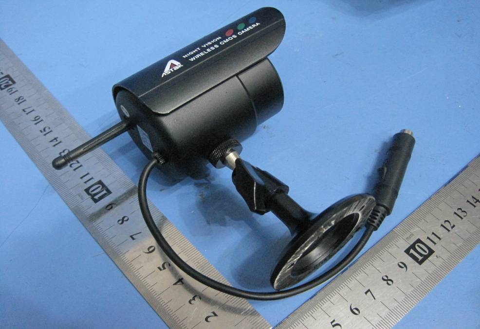
2.1 EUT - Front View 2.2 EUT - Back View
Astak, Inc. FCC ID: W8M-CM-818C2 Page 33 of 33 Ref No.: WT10073060-S-E-F 13 FCC ID Label This device complies with Part 15 of the FCC Rules. Operation is subject to the following two conditions: (1) this device may not cause harmful interference, and (2) this device must accept any interference received, including interference that may cause undesired operation The Label must not be a stick-on paper. The Label on these products must be permanently affixed to the product and readily visible at the time of purchase and must last the expected lifetime of the equipment not be readily detachable. Proposed Label Location on EUT EUT Bottom View/proposed FCC Mark Location FCC ID:W8M-CM-818C2 This device complies with Part 15 of the FCC Rules. Operation is subject to the following two conditions: (1) this device may not cause harmful interference, and (2) this device must accept any interference received, including interference that may cause undesired operation
FCC ID Label Sample for Model :CM-818C2 FCC ID : W8M-CM-818C2 This device complies with Part 15 of the FCC Rules. Operation is subject to the following two conditions:(1)this device may not cause harmful interference, and (2) this device must accept any interference received, including interference that may cause undesired operation.
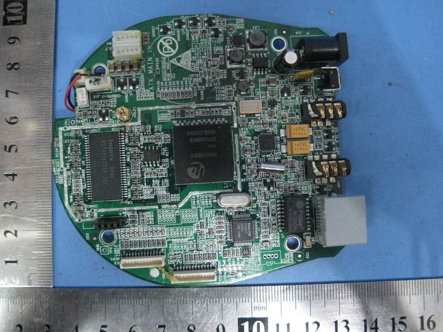
2.1 PCB1- Front View 2.2 PCB1 - Back View 2.3 PCB2- Front View 2.4 PCB2 - Back View 2.5 PCB3- Front View 2.6 PCB3 - Back View
CM-818C2 Camera Circuit Description CM-818C2 Camera Transmitter Block Diagram circuit description Circuit Description The transmitter is made up of two parts: Audio & Video unit and RF unit. The audio signal from MIC is amplified, then modulates the audio carry frequency oscillator (17.7344MHz), the modulated carry frequency is a added in the VT of voltage controlled oscillator VCO (2.4GHz, D1, Q2 ). The video signal from CMOS camera passes through the sharp network (R22、C24,R7、C23), also is added in the VT of VCO another signal is a added in the VCO is the error. Voltage output of loop filter , of PLL(IC1) which is programmed by CPU (IC2) the channel data is decided by the encodes switch (SW1) of CPU peripheries. The feed back signal (R16、 R6, C16) form Voltage controlled oscillator. VCO is compared with reference crystal oscillator the error frequency of oscillator VCO can be corrected. The carry frequency to be modulated by audio & video has been power amplified by Q3 filtered through the band pass filter (C17、C18 microstrip) which the higher harmonica of signal reduced to lower level. The purer signal is emitted by antenna (RF OUT).
1 1 2 2 3 3 4 4 DD CC BB AA Title NumberRevisionSize A4 Date:2010-7-25Sheet of File:G:\2010-07-FCC认证资料\..\TX24G-V2.SCHDOCDrawn By: 1K R20 4K7 R21 100R R22 2K2R3 270K R6 18R R23 12K R9 1K R7 100K R8 1K R11 10K R16 10K R7 7K5 R14 100R R15 33R R17 33K R19 300R R16 10K R21 33R R18 102 C20 102 C22 200pF C24 105 C19 120pF C2 684 C23 475 C7 25P C4 82P C21 104 C16 104 C5 120P C12 3P3 C9 1P5 C10 24PF C28 105 C26 1P5C13 105 C1 120P C15 0P5 C14 3pF C16 24PF C27 1p5 C17 1P5 C18 120P C3 12 17.7344M Y N43 Q3 N48 Q2 3904 Q1 150J L1 A Audio-I/P B 5V--- I/P GND GND C Video-I/P 10K VR1 7K5 R12 100R R13 K N D1 12345678 9 10111213141516 * 1234567 89 1011121314 * +5 NC NC 10K R20 CH / SW 300R R4 NC NC NC 100pF C25 1 CM-818-202 WYX CM-818 2.4G RF.TX A B 0 EM78P153 8170 oscout oscin vp vcc DO GND Xfin fin clock data LE PS R P LD/foutZC P50P67 P66 p63//Rst p64/osco p65/osc1 VDD p62/Tcc p61 p60//INT Vssp53 p52p51 A/0 ANT CH/SW= A & B=0 1CH A =0 2CH B =0 3CH A & B=NC 4CH 104 C11 PDF 文件使用 "pdfFactory Pro" 试用版本创建 www.fineprint.cn 1 1 2 2 3 3 4 4 DD CC BB AA Title NumberRevisionSize A4 Date:2010-7-25Sheet of File:G:\2010-07-FCC认证资料\..\CM-818W.SCHDOCDrawn By: 3904 Q1 104 C2 10K R4 MIC DGND 19 FSI 20 GAMMA 21 SIO-C 26 VHS/MIR 22 SIO-D 27 FODD/HGAIN 23 AWBIS 28 PWDN 24 AGND 1 FASTB 25 AVDD 2 ABRT 3 BKLT 4 DVDD 18 XCLK2 17 OVDD 11 XCLK1 16 VPXONFLP 15 NC 5 SCCB-E 14 VREQ 6 EGND 13 VRCHG 7 EVDD 12 NC 8 NC 9 CVO 10 U1 VinVout GND IC2 78L05 DC JACK 8v in +5 10K R8 10K R6 10K R3 +5 1M R1 33pF C12 33PF C11 +5+5 18R R12 10UF C16 4.7K R17 100K R19 102 C1 104 C8 10K R18 105 C14 A AUDIO O/P CM-818 CAMERA 1:1 A/0CM-818-201 14.31818 X1 3904 Q2 3904 Q3 33K R8 33K R7 2.2K R5 100uF C17 100uF C9 100uF C1 DS DS DS DS DS DSDS DS DS 56R R1 56R R2 56R R3 3906 Q1 IR1 4.7K R6 DSDSDS 1K R010 25PFC3 10K R9 47K R11 36K R10 3904 Q2 3.3K R16 680R R14 3906 Q4 75R R2 100R R13 270R R15 +5 Video o/p 104 C4 3.3K R5 WYX 120R R011 200PF C011 C VIDEO OUTPUT 1K VR1 B 5V O/P D GND PDF 文件使用 "pdfFactory Pro" 试用版本创建 www.fineprint.cn
Astak, Inc. FCC ID: W8M-CM-818C2 FCC TEST REPORT Page 1 of 33 Ref No.: WT10073060-S-E-F FCC ID : W8M-CM-818C2 Applicant : Astak, Inc. Address :1911 Hartog Drive, San Jose, California 95131. USA Equipment Under Test (EUT) : Product description : Wireless Camera Model No. : CM-818C2 Modulation : FM Standards : FCC 15 Paragraph 15.249 Date of Test : Aug 05.2010 Test Engineer : Olic.huang Reviewed By : PERPARED BY: Waltek Services (Shenzhen) Co., Ltd. 1/F, Fukangtai Building, West Baima Rd.,Songgang Street, Baoan District, Shenzhen, China Tel: +86-755-27553488 Fax: +86-755-27553868 Astak, Inc. FCC ID: W8M-CM-818C2 Page 2 of 33 Ref No.: WT10073060-S-E-F 2 Contents Page 1 COVER PAGE..........................................................................................................................................................1 2 CONTENTS ...............................................................................................................................................................2 3 TEST SUMMARY .....................................................................................................................................................4 4 GENERAL INFORMATION ...................................................................................................................................5 4.1 CLIENT INFORMATION..........................................................................................................................................5 4.2 GENERAL DESCRIPTION OF E.U.T. .......................................................................................................................5 4.3 DETAILS OF E.U.T................................................................................................................................................5 4.4 DESCRIPTION OF SUPPORT UNITS.........................................................................................................................5 4.5 STANDARDS APPLICABLE FOR TESTING...............................................................................................................5 4.6 TEST FACILITY.....................................................................................................................................................6 4.7 TEST LOCATION...................................................................................................................................................6 5 EQUIPMENT USED DURING TEST .....................................................................................................................7 6 CONDUCTED EMISSION TEST............................................................................................................................8 6.1 TEST EQUIPMENT.................................................................................................................................................8 6.2 TEST PROCEDURE.................................................................................................................................................8 6.3 CONDUCTED TEST SETUP.....................................................................................................................................9 6.4 EUT OPERATING CONDITION...............................................................................................................................9 6.5 CONDUCTED EMISSION LIMITS...........................................................................................................................10 6.6 CONDUCTED EMISSION TEST RESULT................................................................................................................10 6.7 CONDUCTED EMISSION TESTSETUP VIEW..........................................................................................................12 7 RADIATION EMISSION TEST ............................................................................................................................13 7.1 TEST EQUIPMENT...............................................................................................................................................13 7.2 MEASUREMENT UNCERTAINTY..........................................................................................................................13 7.3 TEST PROCEDURE...............................................................................................................................................13 7.4 RADIATED TEST SETUP......................................................................................................................................14 7.5 SPECTRUM ANALYZER SETUP............................................................................................................................14 7.6 CORRECTED AMPLITUDE & MARGIN CALCULATION..........................................................................................15 7.7 SUMMARY OF TEST RESULTS.............................................................................................................................15 7.8 EUT OPERATING CONDITION.............................................................................................................................16 7.9 RADIATED EMISSIONS LIMIT..............................................................................................................................16 7.10 RADIATED EMISSIONS TEST RESULT..................................................................................................................17 8 ANTENNA REQUIREMENT. ...............................................................................................................................23 9 20-DB BANDWIDTH ..............................................................................................................................................23 10 BAND EDGE........................................................................................................................…
Text truncated - open the document above for the full version.
Conducted Emission Testsetup View Testsetup Front View Testsetup Back View 2.1 Radiation Emission Test View For 30MHz-1000MHz 2.2 Radiation Emission Test View For 1GHz-25GHz
| # | Rule Parts | Frequency Range | Power Output |
|---|---|---|---|
| 1 | 15C | 2.41 GHz - 2.47 GHz | - |

IP CAMERA
Equipment Class
JBP - Part 15 Class B Computing Device Peripheral