WFZSCND502E1233FILMSCAN35 MODERN BASIC
EU3C COMPANY LIMITED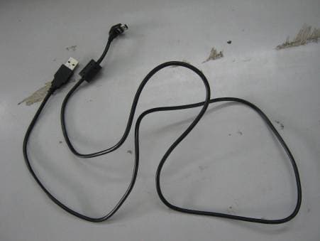
Click to zoom
Application Details
- Equipment Class
- JBP - Part 15 Class B Computing Device Peripheral
- Date of Grant
- Jun 23, 2010
- Application Purpose
- Original Equipment
- Date of Application
- Jun 23, 2010
- Equipment Note
- FILMSCAN35 MODERN BASIC
- Company
- EU3C COMPANY LIMITED
- Country
- Hong Kong
Documents & Files
Document Text
Text extracted from the exhibit documents filed with the FCC. Open a document above to read the original.
Users Manual
User Manual innovativetechnology ITNS-400 -1- Note This film scanner supports Windows XP, Vista/Windows7 (32/64bits) via USB 2.0 only. We strongly suggest using a clean, dry, non-alcohol cotton swab to insert into the film scanner slot and clean the glass surface periodically to produce a clear image. Make sure all negative films, slide films, and cover trays are free of dust and dirt before inserting into the ITNS-400 as this may affect the image quality when scanning. When cleaning films, please use a professionally recommended purger from a photo store to avoid damaging old or precious films. I. Unpack the ITNS-400 Quick Installation Guide ITNS-400 User Manual II. Driver Installation 1. Turn on the computer 2. Insert the installation CD into the CD-ROM drive and the installation CD menu will appear. 3. Choose Installation. To use the ITNS-400, please complete the following installation in advance. -2- 4. Follow the on-screen instructions. (Windows XP, Vista/Windows7) -3- -4- -5- -6- 5. After completing software installation, please connect ITNS-400 to PC. The New Hardware Wizard will detect a new device. -7- 6. Select “Yes” in XP or “Locate and install driver software (recommended)” in Vista/Windows7 OS. -8- -9- 7. After completing the installation, the filmscanner is ready to start with “35mm FilmScanner” Image Scan Tool under program files. (Windows XP, Vista/Windows7 Restart is not required, but it is recommended to restart your PC after installation/un-installation. ) III. Using the ITNS-400 Power status LED Copy button USB Cable Film Slot Installing film into the film holder Install slide Film into the holder entitled “Slides Only” 1. Open the slide holder as illustrated -10- 2. Place slide in recessed slot in holder3. Close the film holder Install Negative Film into the holder entitled “Negative Film Only”: 1. Open the film holder as illustrated 2. Install film into negative film slot 3. Close the film holder Note To avoid a mirror image, follow the serial numbers (from left to right) on top of film when installing negative film into holder. Figure 1 If the image is upside down [see fig.2], the image can be corrected by “Rotate” function in Image Scan Tool after capture [see fig.3]. Figure 2 Figure 3 -11- How to use ITNS-400 1. Put Film into film holder 2. Insert the film holder into the right side of the ITNS-400 unit -12- -13- 3. Connect ITNS-400 to PC 4. Click “Image Scan Tool” to enter operation interface as below -14- 5. Press “Copy” button to capture the image 6. Process necessary modification by function buttons in right hand side -15- 7. Save captured images to PC 8. Get fimal images from PC for further review and edit -16- User interface introduction When user selects a “Negative” source, the image in “Live View” window will be exactly like the processed result. -17- If device processes a slide, the “Live View” will show a color image and the FilmType will remain the same. This is the live view under black and white negative option. -18- User can convert images from traditional film to digital either by “Snap Shot” button in Image Scan Tool or the button on top of filmscanner. Then, the capture result will appear in the “Snap Shot” and “Final images to save” window. All of the effects in Image Scan Tool will be ready for instant preview in “Snap Shot” and “Final images to save” window. Touch button -19- Apply the Mirror function by pressing the “Mirror” icon, that will flip the image and be shown in the “Snap Shot” window as well as the “Final images to Save”. Or apply the Rotate function by pressing “Rotate” button, the image will be rotated 90 degrees each time. Images can be continuously rotated a full 360 degrees or until desired. If the user wishes to delete a specific image from the capture pool, simply click the image under “Final image to save” again, then the selected image can be deleted by applying the “Delete” button. After modification, user can save images to the default location at “C:\Documents and Settings\Users\My Documents\My Pictures”. -20- Once press “Save” key, all of captures images will be saved into defined location. The “final image” saving window shall be empty after press the “Save” button. -21- Or define preferable location for saving captures images by pressing the directory button. Another window will pop out for user to select required location. When the capture is complete, the user can press “Exit” button to quit this Image Scan Tool, Then, review captured images or process more fancy modification with bundle software for PC. -22- -23- IV. Specification Image Sensor:5 mega CMOS sensor Lens:F no.=2.0, 4 Glass elements, Focus Range: Fixed focus Exposure Control: Automatic Color Balance Automatic Scan Quality 1,800 dpi /3600 dpi (SW interpolation) Data Conversion 10 bits per color channel Scan Method Single pass Light Source Back light (3 white LEDs) Interface: USB 2.0 Power: USB port Dimensions W100.6 x L90.5 x H150.3mm Weight 0.39kg Operating Systems Windows XP/Vista/Windows 7 -24- V. Cleaning the ITNS-400 Please remove the film holder from device when you notice any dust in the live view window. Then you can use the cleaning brush to wipe away dust. Note We strongly suggest using a clean, dry, non-alcohol cotton swab to clean the glass surface periodically to produce a clear image during operation. .‐ . .( ‐):\\. .., . Question 1. How to install ITNS‐400 driver? Solution: 01Put FilmScan Driver CDROM into your CD player 02Open the X CDROMDriver folder 03Click mouse right buttonon setup exeand click “Run as administrator” to install driver : -25- ITNS-400 Trouble shooting 04 The InstallShield Wizard will show the message of “InstallShield Wizard Completed once the driver installed ready . . 05 Connect ITNS-400 to your PCthe PC will complete the device driver installation and confirm driver installed successfully ., . -26- Question 2. Came up the error message “Cannot Install This Hardware” or Can not find camera. Please connect your manuf…
Text truncated - open the document above for the full version.
Cover Letter(s)
香 港 商 泛 欧 电 子 通 路 股 份 有 限 公 司 EU3C Company Limited Add: Unit 7, 8/F., Austin Tower, 22-26 Austin Avenue, Tsim Sha Tsui, Kowloon, Hong Kong Tel: 852-2302-4811 Fax: 852-2302-4911 FCC ID: WFZSCND502E1233 Power of Attorney June-20-2010 Federal Communications Commission Authorization and Evaluation Division 7435 Oakland Mills Road Columbia, MD 21046 To Whom It May Concern: We, the undersigned, hereby authorize Guangzhou Huesent Testing Service Co., Ltd. ( Jerry Chen ) on our behalf, to apply to the Federal Communications Commission on our equipment. Any and all acts carried out by Guangzhou Huesent Testing Service Co., Ltd. on our behalf shall have the same effect as acts of our own. This authorization expires on June-20-2011 This is to advise that we are in full compliance with the Anti-Drug Abuse Act. We, EU3C Company Limited, are not subject to a denial of federal benefits pursuant to Section 5301 of the Anti-Drug Act of 1988, 21 USC853a, and no party to the application is subject to a denial of federal benefits pursuant to that section. Sincerely, Letty Lee ( Senior Internal Controller )
External Photos
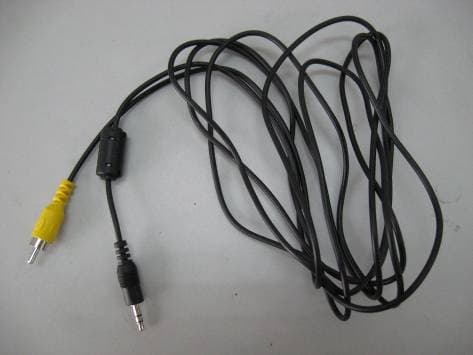
External Photographs of FCCID: WFZSCND502E1233 Page 1 of 2 Page 2 of 2
ID Label/Location Info
FCC ID (WFZSCND502E1233) Label Location FCC ID Label Page 1 of 1
ID Label/Location Info
FCC ID: WFZSCND502E1233 This device complies with Part 15 of the FCC Rules. Operation is subject to the following two conditions: (1) this device may not cause harmful interference, and (2) this device must accept any interference received, including interference that may cause undesired operation.
Internal Photos
Internal Photographs of FCCID: WFZSCND502E1233 Page 1 of 10 Page 2 of 10 Page 3 of 10 Page 4 of 10 Page 5 of 10 Page 6 of 10 Page 7 of 10 Page 8 of 10 Page 9 of 10 Page 10 of 10
Operational Description
Version 1.1, November 30, 2005Proprietary to OmniVision Technologies1 Advanced Information Preliminary Datasheet OV550-B49 Camera Bridge Processor O mniision ® General Description The OV550 Camera Bridge Processor is a low cost, enhanced single-chip processor for USB 2.0 PC camera applications, capable of supporting up to 5.0 Megapixel sensors for game console applications. When combined with an OmniVision VGA, 1.3 Mpixel, 2.0 Mpixel, 3.2 Mpixel, or 5.0 Mpixel digital C AMERACHIP™, the OV550 comprises an integrated USB 2.0 camera system, with no additional USB transceiver or DRAM required. The OV550 also supports full video operation. Features General Features •Low cost, low powered image processor that supports up to 5.0 Megapixel sensors •Maximum pixel clock running at 48 MHz: 30 fps for 1.3MP Raw mode, 15 fps for 1.3MP YUV mode •Supports USB Video Class with uncompressed format •Serial Camera Control Bus (SCCB) Master Controllers CAMERACHIP Interfaces •Up to 5 Megapixel •10-bit RGB interface •8-bit YUV interface Host Interface - USB 2.0 •Supports USB Video Class with uncompressed format •Supports both isochronous and bulk endpoint for video transfer Embedded 8-bit Microcontroller •Embedded 512-Byte data memory •Embedded 12KB program memory Miscellaneous •Embedded 3.3V to 1.8V regulators •Embedded PLL •Optional external serial EEPROM •General Purpose I/O (GPIO) •Power-down control Ordering Information Pb Note: The OV550-B49 is available in a lead-free package. ProductPackage OV0550-LB30BGA-49 (Lead-free) Applications •USB 2.0 applications combined with the following OmniVision C AMERACHIP families: –OV56xx (5.0 MegaPixel) –OV36xx (3.2 MegaPixel) –OV26xx (2.0 MegaPixel) –OV96xx (1.3 MegaPixel) –OV86xx (SVGA) –OV76xx (VGA) –OV66xx (CIF) NOTE: The OV550 supports digital image sensors up to 5.0 Megapixel resolution. However, it will not support analog image sensors (OVx9xx or OVx4xx products) Key Specifications Figure 1 OV550-B49 Pin Diagram Power Supply Core1.8 V I/O3.3V Regulator Input3.3V Power Requirements ActiveTBD StandbyTBD Temperature RangeTBD Package Dimensions6.00 mm x 6.00 mm 76 5 4 321 AIO_VDD2OSCENTMGPIO1GPIO0SIO_CSIO_D BRESET_GPIO4IO_VSS2IO_VDD1Y[1]Y[0]GPIO2 CXINXOUTCORE_VSS2Y[4]Y[3]Y[2]IO_VSS1 DUSB_VSSA2VRESCORE_VDD2PCLKCORE_VSS1CCLKY[5] EUSB_VDDL USB_VSSL USB_VDDA2Y[8]Y[7]Y[6]CORE_VDD1 FDMUSB_VSSA1 USB_VDDDSPWDNVSYNCHREFY[9] GDPRPUUSB_VDDA1 ROUT_VDD1 REG_VSS18 RIN_VDD18GPIO3 1234567 A B C D E F G 2Proprietary to OmniVision TechnologiesVersion 1.1, November 30, 2005 OV550-B49Camera Bridge Processor O mniision Functional Description Figure 2 shows the functional block diagram of the OV550 processor. The OV550 includes: •Camera Interface •USB Converter •Host Controller •SCCB Master Controller •Microcontroller •System Controller Camera Interface The Camera Interface takes either 10-bit RGB raw data or 8-bit YUV data from a maximum 5 Megapixels image sensor. The maximum pixel clock runs at 48MHz to support 30 fps for 1.3 Megapixel RAW mode or 15 fps for 1.3 Megapixel YUV mode. The Camera Interface can interface with the image sensor CCIR656 and CCIR601 modes. Host Controller The OV550 uses USB2.0 to communicate with the Host Controller and supports USB video class with uncompressed format. SCCB Master Controller The SCCB Master Controller controls sensor registers. It is possible for the SCCB Master Controller to interface with an optional external EEPROM for downloading firmware to the program memory of the Microcontroller when the system is powered up. Microcontroller The OV550 is embedded with an 8-bit microcontroller with 512-Byte data memory and 12KB program memory. It provides the flexibility of decoding protocol commands from the host for controlling the system, as well as fine-tuning image qualities. System Controller The System Controller provides some system functions, such as GPIO and power down functions. Figure 2 Functional Block Diagram Data Path Came ra Interface Host UDC USB MC Se r ial E 2 prom SCCB M aster RGB 10-bit YUV 8-bit OV x6xx Vide o FIFO UDCIF Syste m Re giste r Bus Syste m Controller GPIO Pin Description Version 1.1, November 30, 2005Proprietary to OmniVision Technologies3 O mniision Pin Description Table 1 Pin Description by Function Ball NumberNamePin TypeFunction/Description System Control F4SPWDNI/O Sensor Power Down General Purpose I/O Default: Output 1 A3GPIO0I/O General Purpose I/O Audio interface synchronization signal Default: Output 0 A4GPIO1I/O General Purpose I/O Audio interface clock signal Default: Output 1 B1GPIO2I/O General Purpose I/O Default: Input G1GPIO3I/O General Purpose I/O Default: Input B6GPIO4I/O General Purpose I/O Default: Input B7RESET_Input Power On Reset 0:Reset C6XOUTOutputCrystal Output C7XINInputCrystal Input A5TMInputTest Mode Enable A6OSCENOutputCrystal Enable Camera Interface B2Y[0]I/O Sensor Data Y[0] General Purpose I/O Default: Input of sensor data Y[0] B3Y[1]I/O Sensor Data Y[1] General Purpose I/O Default: Input of sensor data Y[1] C2Y[2]I/O Sensor Data Y[2] General Purpose I/O Default: Input of sensor data Y[2] C3Y[3]I/O Sensor Data Y[3] General Purpose I/O Default: Input of sensor data Y[3] 4Proprietary to OmniVision TechnologiesVersion 1.1, November 30, 2005 OV550-B49Camera Bridge Processor O mniision C4Y[4]I/O Sensor Data Y[4] General Purpose I/O Default: Input of sensor data Y[4] D1Y[5]I/O Sensor Data Y[5] General Purpose I/O Default: Input of sensor data Y[5] E2Y[6]I/O Sensor Data Y[6] General Purpose I/O Default: Input of sensor data Y[6] E3Y[7]I/O Sensor Data Y[7] General Purpose I/O Default: Input of sensor data Y[7] E4Y[8]I/O Sensor Data Y[8] General Purpose I/O Default: Input of sensor data Y[8] F1Y[9]I/O Sensor Data Y[9] General Purpose I/O Default: Input of sensor data Y[9] D2CCLKI/O Camera Clock to Sensor General Purpose I/O Default: Output of camera clock D4PCLKI/O Pixel Clock from Sensor General Purpose I/O Default: Input of pixel clock F2HREFI/O Horizontal Reference/Sync from Sensor General Pu…
Text truncated - open the document above for the full version.
Parts List/Tune Up Info
ItemComponent No.Part Spec Source code Q'tyVer. RoHS L/T Purchasi ng SupplierSearch Insertation location │ └┬─ 8─ 555-FS9KEYR0010Key_B for New FS-I for ITP1RoHS │ ├─ 1─ 203-00KAN0R4400MIC-KAN-04P1RoHSS11 │ └─ 2── 208-FS1KEYR0010Key_B PCB V1.0P1RoHS │ └─ 3── 290-050020F6000 2PIN distance:1.25mm/No anchor pole 2PIN-SMD-S P1RoHS S1
Schematics
1.1 Benny A3 CHECKED BY: DATE: APPROVED BY:SIZE SHEETDOC. REV. SCH DOC. TYPE PROJ. CODE MODEL NO. EU3C DESCRIPTIONDOC. NO.PCB P/NFILENAMEDESIGNED BY: DRAWN BY: SCHEMATIC OF FilmScaner 1 1 OF 1 DATE: DATE: DATE: Johnny Snap Button POWER CIRCUIT Johnny A1 SDA A2 SCL A3 GPIO0 A4 GPIO1 A5 TM A6 OSCEN A7 IO_VDD2 B1 GPIO2 B2 Y0 B3 Y1 B4 IO_VDD1 B5 IO_VSS2 F2 HREF F1 Y9 E7 VDDL E6 VSSL E5 VDDA2 E4 Y8 E3 Y7 E2 Y6 E1 CORE_VDD1 D7 VSSA2 D6 VRES D5 CORE_VDD2 F3 VSYNC F4 SPWDN F5 VDDD F6 VSSA1 F7 DM G1 GPIO3 G2 RIN_VDD G3 REG_VSS G4 ROUT_VDD G5 VDDA1 G6 RPU G7 DP D4 PCLK D3 CORE_VSS1 D2 CCLK D1 Y5 C7 XIN C6 XOUT C5 CORE_VSS2 C4 Y4 C3 Y3 C2 Y2 C1 IO_VSS1 B7 NRESET B6 GPIO4 U1 OV550_49_0.4 5 VIN 3 EN 1 VOUT 4 CN 6 CP 2 GND U7 RT9361B Y1 HC49SMD 12MHz R25 R0603 NC C15C06030.1uF 12345 J8 CON5-2.0 usb jack 1 GND 3 OUT 2 IN U3 SOT89XC62FP3302 S G D Q1 M-SOT-23 12 1 A0 2 A1 3 A2 4 GND 8 VCC 7 WP 6 SCL 5 SDA U2 24LC64 JP2 SW PUSHBUTTON C16 1210 22uF RC1 R06030R R13 R0603 3R3 R14 R0603 3R3 R16 R0603 3R3 C37C06030.1uF 1 GND 3 OUT 2 IN U5 SOT89XC62FP1802 R17 R0603 3R3 R18 R0603 3R3 1 GND 3 OUT 2 IN U4 SOT89XC62FP1302 + C11 6032 100uF C12C06030.1uFC14 C0603 0.1uF + C20 6032 100uF C21C06030.1uF + C18 6032 100uF C19C06030.1uF R8 R0603 1.5K R4 R0603 1M C1C060310P C2C060310P C10C06030.1uF R11R0603 6.2K 1 TP1 TEST POINT C39 C0603 1uF C38120610uF C40120610uF R3 R0603 220R R28 R0603 10k R29 R0603 NC C5C06030.1uF C9C06030.1uF C8C06030.1uF C6C06030.1uF C7C06030.1uF JP1 SW PUSHBUTTON R5 R0603 10k R6 R0603 10k R7 R0603 10k C42C06033pF C41C06033pF R2 R0603 150R R1 R0603 150R R9 R0603 10k R10 R0603 10k C4C06030.1uF S1 SW PUSHBUTTON + A - K D2 IN4148 1 GND 3 OUT 2 IN U9 SOT89XC62FP3302 + C48 C0805 100uF S G D Q2 SOT-23 1 2 3 R80 0 12 RA2 R0603 0R C3120610uF 1 GND 3 OUT 2 IN U8 SOT89XC62FP2802 C47C06030.1uF C43C06030.1uF C44 C060333PF OV5620CLCC 6 NC1 7 NC2 8 NC3 9 PWDN 10 FREX 11 RESET 12 EXPST 13 Y0 14 Y1 15 Y2 16 Y3 17 NC4 18 NC5 31 NC7 32 NC8 33 DVDD 34 Y4 35 Y5 36 Y6 37 Y7 38 Y8 39 Y9 40 PCLK 41 NC9 42 NC10 43 VSYNC 44 HREF 45 SCL 46 SDA 47 SVDD 48 AGND 1 DOVDD 2 STROBE 4 VREF1 5 VREF2 3 RVDD 19 NC6 20 EVDD 21 CLKP 22 CLKN 23 DATAP 24 DATAN 25 EGND 26 PVDD 27 XVCLK 28 DOGND 29 AVDD 30 DGND U10 OV5620CLCC R24 R0603 0R R31 R0603 0R C32 C060333PF C30 C0603 33PF C35 C06031uF C31 C06030.1uF C36 C06030.1uF C34 C06030.1uF C33 C06030.1uF C24C06031uF R22 R0603 10k C28C06030.1uF C22 C0603 0.1uF C45 C0603 0.1uF C29 C0603 0.1uF C27 C0603 0.1uF C23 1210 22uF C17 1210 22uF + C46 6032 100uF + C13 6032 100uF R19 R0603 Na R26 R0603 NA C26 C060333PF 1 1 2 2 3 3 4 4 LB COMMON CHOKE 1206 260OHM R20 60R@100MHz 800mA R21 60R@100MHz 800mA R0 60R@100MHz 800mA LA 30R@100MHz 500mA L3 60R@100MHz 800mA RA1 60R@100MHz 800mA RB1 60R@100MHz 800mA L4 60R@100MHz 800mA L2 60R@100MHz 800mA L1 60R@100MHz 800mA R12 60R@100MHz 800mA R15 60R@100MHz 800mA R30 60R@100MHz 800mA R23 R0603 100R R32 R0603 100R Y0 Y1 Y2 Y3 Y4 PCLK Y5Y6Y7 Y8 Y9 VSYNC HREF C_SIO_D U5.0V VSS DGND AGND DGND GPIO1 RPU DP DM RPU HREF VSYNC PCLK SNAPSHOT RESET# VSS FLIP VSS GND GND Y9Y8Y7Y6Y5Y4Y3Y2Y1Y0 CCLK S_PWDNOSC_ENLED GPIO1 C_SIO_D C_SIO_C EN VSS C_SIO_C C_SIO_D U5.0V DM DP LED RESET# SNAPSHOT IO_VDD CORE_VDD USB_VDDA USB_VDDL USB_VDDD D3.3V USB_VDDL CORE_VDD USB_VDDA USB_VDDD IO_VDD AVDD DVDD RVDD DOVDD DGND D3.3V S3.3V D1.8V USB_VDDD IO_VDD CORE_VDD USB_VDDA USB_VDDL USB_VDDD D3.3V D3.3V S3.3V D3.3V S3.3V C_SIO_C C_SIO_D IO_VDD S5.0V FLIP OSC_EN S5.0V SEN_PWR S5.0V EVDD DGND DGND AVDD C_SIO_C AGND DOVDD RVDD DGND DGND S_PWDN DGND DOVDD DGND EVDD RVDD AVDD AGND DVDD DGND CCLK GND GND RSTB GND AGND GND GND GND
Test Report
FCCID: WFZSCND502E1233 Report Number: HST201006-2376-FCC-E Page 1 of 23 Test Report Applicant: EU3C Company Limited Address of Applicant: Unit 7, 8/F., Austin Tower, 22-26 Austin Avenue, Tsim Sha Tsui, Kowloon, Hong Kong Equipment Under Test (EUT): EUT Name: FilmScan35 Modern Basic Model No.: SCND502E1233 Serial No.: Not supplied by client Standards: FCC PART15 SUBPART B: 2007 Date of Receipt: Jun. 12, 2010 Date of Test: Jun. 12, 2010 – Jun. 13, 2010 Date of Issue: Jun. 15, 2010 Test Result : PASS* * In the configuration tested, the EUT complied with the standards specified above. Authorized Signature: Henly.xie / Manager This report refers to the General Conditions for Inspection and Testing Services, printed overleaf This report details the results of the testing carried out on one sample. The results contained in this test report do not relate to other samples of the same product. The manufacturer should ensure that all products in series production are in conformity with the product sample detailed in this report. This report may only be reproduced and distributed in full. If the product in this report is used in any configuration other than that detailed in the report, the manufacturer must ensure the new system complies with all relevant standards. The report must not be used by the client to claim product certification, approval, or endorsement by NVLAP, NIST, or any agency of the federal government. All test results in this report can be traceable to National or International Standards. The test report prepare by: Guangzhou Huesent Testing Service Co., Ltd. No.91, Dongguanzhuang Road, Guangzhou, China. Tel: 86-20-28263298 Fax: 86-20-28263237 http://www.hst.org.cn E-mail:[email protected] Report Number: HST201006-2376-FCC-E Page 2 of 23 2. Test Summary Test Test RequirementTest Method Class / Severity Result Radiated Emission (30MHz to 1GHz) FCC PART 15, SUBPART B: 2007 ANSI C63.4:2003 Class B PASS Conducted Emission (150KHz to 30MHz) FCC PART 15, SUBPART B: 2007 ANSI C63.4:2003 Class B PASS Report Number: HST201006-2376-FCC-E Page 3 of 23 3. Contents TITLE ........................................................................................................................PAGE 1. COVER PAGE......................................................................................................................1 2. TEST SUMMARY......................................................................................................................... 2 3. CONTENTS .................................................................................................................................. 3 4. GENERAL INFORMATION ..........................................................................................................4 4.1 CLIENT INFORMATION........................................................................................................... 4 4.2 GENERAL DESCRIPTION OF E.U.T......................................................................................... 4 4.3 DETAILS OF E.U.T................................................................................................................ 4 4.4 DESCRIPTION OF SUPPORT UNITS......................................................................................... 4 4.5 STANDARDS APPLICABLE FOR TESTING................................................................................. 4 4.6 TEST LOCATION................................................................................................................... 4 4.8 DEVIATION FROM STANDARDS............................................................................................... 4 4.9 ABNORMALITIES FROM STANDARD CONDITIONS..................................................................... 4 5. EQUIPMENTS USED DURING TEST.......................................................................................... 5 6. TEST RESULTS ........................................................................................................................... 6 6.1 CONDUCTED EMISSIONS MAINS TERMINALS, 150 KHZ TO 30MHZ............................................... 6 6.1.1 E.U.T. Operation ............................................................................................................. 6 6.1.2 Plan View of Test Setup..................................................................................................6 6.1.3 Measurement Data..........................................................................................................6 6.2 RADIATED EMISSIONS, 30MHZ TO 1GHZ................................................................................... 9 6.2.1 E.U.T. Operation ............................................................................................................. 9 6.2.2 Test Setup ....................................................................................................................... 9 6.2.3 Measurement Data..........................................................................................................9 7. PHOTOGRAPHS ........................................................................................................................ 12 7.1 CONDUCTED EMISSION TEST SETUP........................................................................................ 12 7.2 RADIATED EMISSION TEST SETUP............................................................................................ 13 7.3 EUT CONSTRUCTIONAL DETAILS............................................................................................. 14 Report Number: HST201006-2376-FCC-E Page 4 of 23 4. General Information 4.1 Client Information Applicant: EU3C Company Limited Address of Applicant: Unit 7, 8/F., Austin Tower, 22-26 Austin Avenue, Tsim Sha Tsui, Kowloon, Hong Kong 4.2 General Description of E.U.T. EUT Name: FilmScan35 Modern Basic Trade Name: EU3C Item No.: See the model number shown on cover page. Serial No.: Not supplied by client 4.3…
Text truncated - open the document above for the full version.
Test Setup Photos
Setup Photographs of FCCID: WFZSCND502E1233 CE Page 1 of 2 RE Page 2 of 2
Contact Information
Applicant
LETTY LEE(SENIOR INTERNAL CONTROLLER)
Test Firm
China CEPREI LaboratoryLihui Chen
Technical Specifications
| # | Rule Parts | Frequency Range | Power Output |
|---|---|---|---|
| 1 | 15B | - | - |
Other Applications from EU3C COMPANY LIMITED
WFZSCND502B1232
Apr 12, 2011PART 15 CLASS B COMPUTING PERIPHERAL
Equipment Class
JBP - Part 15 Class B Computing Device Peripheral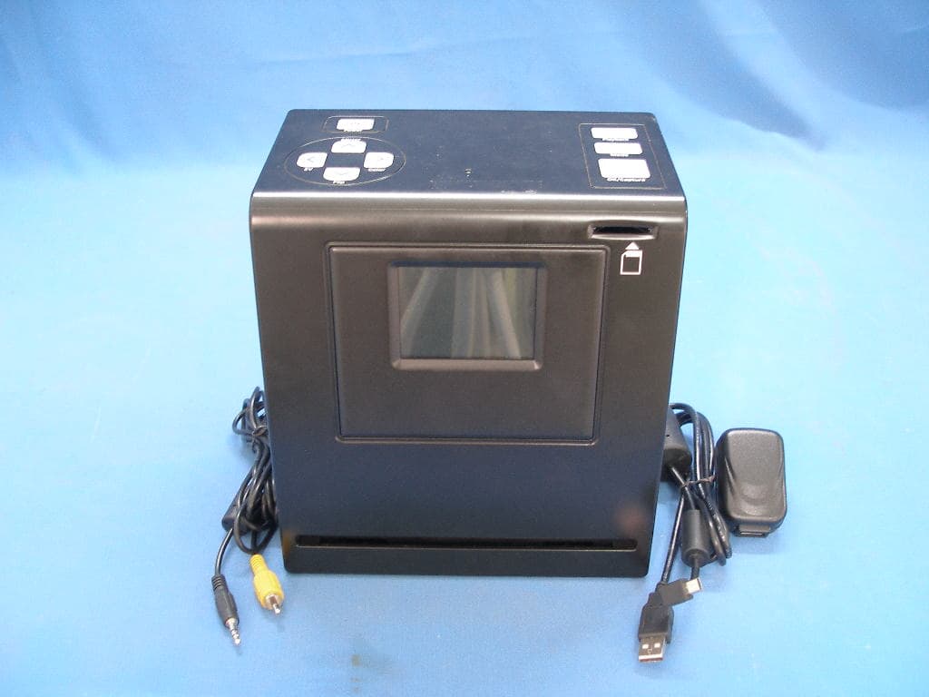
WFZSCND503H1231
Mar 28, 2011CS-II-5M-3.0
Equipment Class
JBP - Part 15 Class B Computing Device Peripheral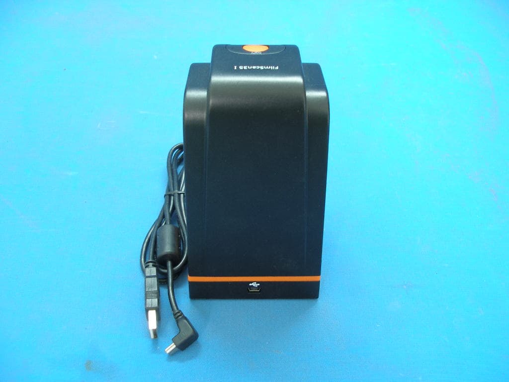
WFZSCND522A1231
Mar 28, 2011FS-I-5M-ND
Equipment Class
JBP - Part 15 Class B Computing Device Peripheral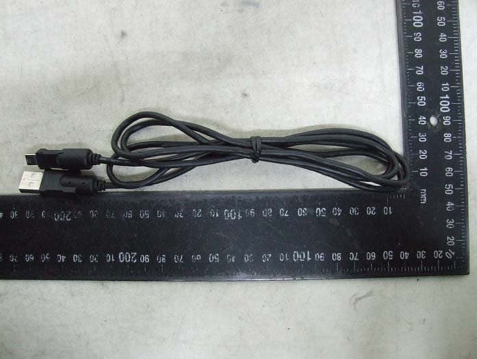
WFZBCS200211011
Mar 24, 2011Businesscardscanner Foldable
Equipment Class
JBP - Part 15 Class B Computing Device Peripheral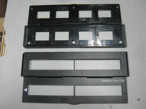
WFZSCND502E1234
Mar 22, 2011PART 15 CLASS B COMPUTING PERIPHERAL
Equipment Class
JBP - Part 15 Class B Computing Device Peripheral