X4TSCT-4VS83-24 PORT VIDEO SERVER
SUNYOUNG ELECTRONIC (SHENZHEN) CO., LTD.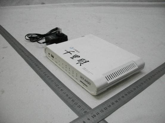
Click to zoom
Application Details
- Equipment Class
- JBP - Part 15 Class B Computing Device Peripheral
- Date of Grant
- Mar 23, 2011
- Application Purpose
- Original Equipment
- Date of Application
- Mar 23, 2011
- Equipment Note
- 4 PORT VIDEO SERVER
- Country
- China
Documents & Files
Document Text
Text extracted from the exhibit documents filed with the FCC. Open a document above to read the original.
Users Manual
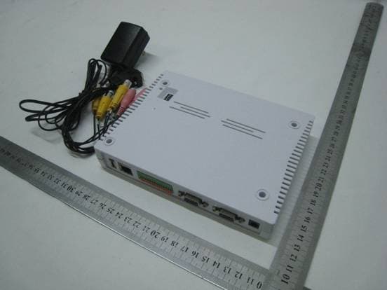
User Manual SCT-4VS83 Changwa Telecom 4 Port Video Server Version 2.0 2011.02.25 Federal Communications Commission(FCC) Statement You are cautioned that changes or modifications not expressly approved by the part responsible for compliance could void the use’s authority to operate the equipment FCC-Class B This equipment has been tested and found to comply with the limits for a Class B digital device, Pursuant to part 15 of the FCC Rules. These limits are designed to provide reasonable protection against harmful interference in a communications. However , these is no guarantee that interference will not occur in particular installation. If this equipment does cause harmful interference to radio or television reception, which can be determined by turning the equipment off and on, the user is encouraged to try to correct the interference by one or more of the following measures: - Reorient or relocate the receiving antenna. - Increase the separation between the equipment and receiver. - Connect the equipment into an outlet on a circuit different from that to which the receiver is connected. - Consult the dealer or an experienced radio/TV technician for help. 一、 Video Server Appearance Explanation Port Description DC IN 12V Power Input Video In & Audio In VidEo IN Audio In/Out Video Out VGA Video Output DI/DO Digital In/Out RS485 RS485 Control port RS232 RS232 Control port INTERNET 10/100/1000 M Internet Port USB USB Port AOUT Audio Out Port SD SD Card 二、 Video Server Installation Explanation 1. How to Link Ethernet:Please connect the Ethernet Cable to plug in the Internet port and connect another end to the Switch or HUB. 2. How to Link Power:Take out the Power Adaptor and connector to 12V Power DC In。 3. When Power On: The power light status is on and system is working。 三、 Digital In/Out & RS485 Port Explanation Port Item Pin Status 1 Digital Input 1(+) 2 Digital Input 1(-) 3 Digital Input 2(+) 4 Digital Input 2(-) 5 Digital Input 3(+) 6 Digital Input 3(-) 7 Digital Input 4(+) 8 Digital Input 4(-) 9 Digital Output 1(+) 10 Digital Output 1(-) 11 Digital Output 2(+) 12 Digital Output 2(-) 13 RS485 (Data +) 14 RS485 (Data -) 15 RS232 (RX) 16 RS232 (TX) Equipment Identity: Digital Input: Max Voltage:DC 24 V Max Electric Current:5mA Digital Output: Max Voltage:DC 30V Max Electric Current:1 A 四、 Video Server LED & Audio Explanation LED Expression Status LED Expression Alarm SD Green Flashlight SD Mistake Red SD Card Status No SD Card N/A Normal Green Flashlight Slowly network N/A Internet Status (ETH) Straming Green Flashlight Speedily System On Always Brightness Alarm voice six times Voice Mute Service Green Light Alarm voice three times Connector to Internet; But system is no action. Orange Light Doesn't have connector to Internet Red Light Work Status (Power) Maintenance mode Flashlight Speedily Alarm voice four times Camera ON Always Brightness Camera OFF N/A Camera Streaming of Video Flashlight Speedily Camera Status (CH1~4) Camera Error Flashlight Slowly No matter issue. N/A Event Status (CH1~4) Have matter issue. Flashlight one times 五、 Obstacle Determine & Processing Error State LED Audio Treatment method Power Off All LED Off N/A Check whether the power is connected well Internet Off Internet Off N/A Check Internet It is normal If it is out of question to join, please change another Network thread test Boot System Error N/A Boot system haven’t alarm six times 30 seconds later.
Block Diagram
8183 8183 DDR Flash TW2865 Flash IC+MCU 4Video in Audio in SD 12MHz
Cover Letter(s)
SUNYOUNG ELECTRONIC (SHENZHEN) Co., Ltd. FCC ID: XCTSCT-4VS83-2 Power of Attorney 2011-03-11 Federal Communications Commission Authorization and Evaluation Division 7435 Oakland Mills Road To Whom It May Concern: We, the undersigned, hereby authorize Most Technology Service Co., Ltd.(Mark Wen/General Manager) on our behalf, to apply to the Federal Communications Commission on our equipment. Any and all acts carried out by Most Technology Service Co., Ltd.(Mark Wen/General Manager) on our behalf shall have the same effect as acts of our own. This authorization will expire on Mar. 16, 2011 This is to advise that we are in full compliance with the Anti-Drug Abuse Act. We, SUNYOUNG ELECTRONIC (SHENZHEN)CO.,LTD are not subject to a denial of federal benefits pursuant to Section 5301 of the Anti-Drug Act of 1988, 21 USC853a, and no party to the application is subject to a denial of federal benefits pursuant to that section. Sincerely SUNYOUNG ELECTRONIC (SHENZHEN)CO.,LTD chris cheng (R&D DIV.Manager) Mar. 11. 2011
Operational Description
OPERATIONAL DESCRIPTION Boot up. Set up and connect network. Start RTSP service procedure and wait for connecting. Start video capture procedure, keep working by Framerate and Birrate which have been set, also connect to RTSP service procedure where offers 4corresponding video channel. Start audio sampling procedure, keep working by sample rate which has been set, also connect to RTSP service procedure where offers 4 corresponding audio channel. Get connect video server and video can be running transport, two modes are available— 1)IN TIME RECORDING Once Digital In is triggered which cause corresponding Digital out running and start to transport audio and video frequency to Video Server, also event data can be conveyed in the same time. 2) FULL-TIME RECORDING Video and Audio frequency has been transporting to Video Server, once Digital In is triggered which cause corresponding Digital out running and start to convey related event data.
Schematics
55 44 33 22 11 D D C C B B A A TitleSize Document Number Rev Date: Sheet of <Doc> 1.0 8182 A3 114 Monday, November 08, 2010 TitleSize Document Number Rev Date: Sheet of <Doc> 1.0 8182 A3 114 Monday, November 08, 2010 TitleSize Document Number Rev Date: Sheet of <Doc> 1.0 8182 A3 114 Monday, November 08, 2010 Description Release Version PAGE DVS-0828FINAL.DSN Content Suanmper Owing to the GM8182 is a high speed IC with highspeed DDR2-SDRAM interface, improper PCB layoutwill cause the function fail.From our experience, we found that the GM8182performance and stability is strongly related tothe PCB layout.In order to ensure your system will work whenmaking your own EVB at the first time,please copy the Power/Ground and DDR layout of oursample design into your system.If your PCB layout of the Power/Ground and DDRpart is not identical to our sample design,we may refuse to support your EVB debugging.GM8182 是一顆高速 SoC 晶片 , 並搭配高速之 DDR2 SDRAM 介面 . 不正確的 PCB 繞線 , 會造成 EVB 系統工作不正常 . 從我們多次設計 GM8182 系統經驗 , 發現 GM8182 的性能與穩定性 , 會與 PCB 繞線品質有強烈之關係 . 因此我們會提供客戶 Layout 與 Gerber file 做為參考 . 為了確保客戶在製作屬於自己的 EVB 時 , 第一次就能成功 . 我們要求客戶之 PCB 繞線 , 在 BGA Power/Ground 及 DDR SDRAM 部分 , 要與原廠相同 . 假若客戶之 PCB 繞線與原廠要求不同時 , 基於人力考量 , 我們可能拒絕幫助客戶的 PCB 偵錯工作 55 44 33 22 11 D D C C B B A A TitleSize Document Number Rev Date: Sheet of <Doc> 1.0 8182 A3 214 Monday, November 08, 2010 TitleSize Document Number Rev Date: Sheet of <Doc> 1.0 8182 A3 214 Monday, November 08, 2010 TitleSize Document Number Rev Date: Sheet of <Doc> 1.0 8182 A3 214 Monday, November 08, 2010 Rev Date Page Description/Change List Page Revision Description/Change List Rev Date 123456 78910 11 12 2009.10.21 1V0A 1. Modify USB power and gnd Bead. 2009.10.21 1V0A 1. Modify USB Vref Resistor to 11K. 2009.10.26 1V0B 2. Modify OTG IDDIG circuit. 2009.10.26 1V0B 2. Modify GM8182 SATA power and gnd.2009.10.27 1V1 1. Modify DDR series resistor. 55 44 33 22 11 D D C C B B A A I2C_SCLI2C_SDA SYS_RSTn I2C_SCL CA_PCLK SYS_RSTn I2C_SDA SYS_RSTn DDR_0_DQSn[0..1] DDR_0_CKE0 S2_TXD DDR_1_A[0..13] RxP0 DDR_0_BA[0..2] S3_RXD VGA_BOUT U_DM I2S0_BCLKSMC_OEn DDR_1_DQS[0..1] I2S0_TXD DDR_1_DQM[0..1] DDR_1_CSn0I2C_SDASYS_RSTnI2S0_FSDDR_0_RASnDDR_0_ODT0 ICE_TCK S3_TXD VSYNC_OUT V2_PCLKIDDR_0_CASnDDR_1_CLKn0 DDR_1_DQ[0..15] DDR_1_ODT0 ICE_TMSICE_DBGREQ SMC_CSn0DDR_0_CLKn0 SMC_DQ[0..7] S2_RXD U_PREFU_IDDIG RxN0TxN0 DDR_1_WEn DDR_1_DQSn[0..1] DDR_1_CKE0 S1_RXDS4_RXD U_DM_H V1_DI[0..7] SMC_WEn SMC_ADDR[0..23]DDR_0_DQ[0..15] ICE_TDI DDR_0_WEn DDR_1_BA[0..2] ICE_DBGACK CA_PCLK I2S0_RXD HSYNC_OUTDAC_RSETDAC_IOUTB V1_PCLKII2C_SCL U_VBUS DDR_0_A[0..13] VGA_GOUT DDR_1_RASn ICE_TRSTnVGA_ROUT U_DP_H V2_DI[0..7]DDR_0_DQS[0..1] DDR_0_CSn0 S4_TXDS1_TXDVGA_RSET DDR_1_CASnDDR_1_CLK0 ICE_TDO U_DP TxP0 DDR_0_DQM[0..1] DDR_0_CLK0 MAC_CLKGPIO0MAC_COLMAC_CRSMAC_MDIOMAC_TX_CLK MAC_RXD[0..7] MAC_RX_DVMAC_RX_ERMAC_TX_ENMAC_PHY_LINKMAC_MDCMAC_GTX_CKMAC_PHY_PDMAC_RX_CLK MAC_TXD[0..7] GPIO1GPIO2GPIO3 NAND_CEn0NAND_CEn1 U_DMU_DP SD_CDnSD_CMD_RSPSD_WPn SD_DAT[0..3] SD_CLK PHY_ACT PHY_ACT DAC_IOUTAICE_TMS U_DM_HU_DP_HU_VBUSU_IDDIGU_PREF SYS_RSTn TitleSize Document Number Rev Date: Sheet of <Doc> 1.0 8182 A1 314 Monday, November 08, 2010 TitleSize Document Number Rev Date: Sheet of <Doc> 1.0 8182 A1 314 Monday, November 08, 2010 TitleSize Document Number Rev Date: Sheet of <Doc> 1.0 8182 A1 314 Monday, November 08, 2010 08_CAPTURE108_CAPTURE1 SYS_RSTnI2C_SCLI2C_SDAV1_DI[0..7]V2_DI[0..7]V1_PCLKIV2_PCLKII2S0_BCLKI2S0_FSI2S0_RXDI2S0_TXDCA_PCLKDAC_IOUTAICE_TMS 05_GM818205_GM8182 14_USB/SD14_USB/SD U_DMU_DPSD_DAT[0..3]SD_CMD_RSPSD_WPnSD_CDnSD_CLKU_DP_HU_DM_HU_VBUSU_PREFU_IDDIG 13_Power13_Power SYS_RSTn 07_Flash07_Flash SYS_RSTnSMC_CSn0SMC_DQ[0..7]SMC_OEnSMC_ADDR[0..23]SMC_WEn 06_DDR206_DDR2 DDR_0_DQM[0..1]DDR_1_DQ[0..15]DDR_1_DQSn[0..1]DDR_0_DQS[0..1]DDR_1_ODT0DDR_0_DQSn[0..1]DDR_0_ODT0DDR_0_DQ[0..15]DDR_1_DQM[0..1]DDR_1_DQS[0..1]DDR_0_A[0..13]DDR_1_A[0..13]DDR_0_BA[0..2]DDR_1_BA[0..2]DDR_0_CLK0DDR_0_CLKn0DDR_1_CLK0DDR_1_CLKn0DDR_0_CKE0DDR_1_CKE0DDR_0_CSn0DDR_1_CSn0DDR_0_WEnDDR_1_WEnDDR_1_RASnDDR_0_RASnDDR_0_CASnDDR_1_CASn 11_Display 11_Display DAC_RSET DAC_IOUTB VGA_RSET VGA_ROUT VGA_GOUT VGA_BOUT VSYNC_OUT HSYNC_OUT 09_PANEL09_PANEL SYS_RSTn PHY_ACT S3_TXD S3_RXD 12_MISC12_MISC I2C_SDA ICE_TDO S2_TXDS1_TXDS4_TXD SYS_RSTn I2C_SCL ICE_DBGACK S1_RXDS2_RXDS4_RXD ICE_TRSTn ICE_TDI ICE_TMS ICE_TCK ICE_DBGREQ TxN0 TxP0 RxN0 RxP0 GPIO1GPIO2GPIO3 NAND_CEn0NAND_CEn1 04_GM818204_GM8182 U_IDDIGU_DPU_PREFU_VBUSU_DM SYS_RSTn S4_RXD SD_WPn SD_CMD_RSP SD_DAT[0..3] S2_RXDS1_RXD SD_CDn S3_RXD SMC_DQ[0..7] DDR_0_CLK0 I2C_SDA I2C_SCL S1_TXDS2_TXDS3_TXDS4_TXDICE_TRSTnICE_TDIICE_DBGREQICE_TMSICE_TCKICE_TDOICE_DBGACK SD_CLK DDR_0_ODT0DDR_1_ODT0 DDR_0_CLKn0DDR_1_CLKn0 DDR_1_CLK0 DDR_0_CKE0DDR_1_CKE0 DDR_0_BA[0..2]DDR_1_BA[0..2] DDR_0_CSn0DDR_1_CSn0 DDR_0_DQ[0..15]DDR_1_DQ[0..15] DDR_0_DQS[0..1] DDR_0_DQSn[0..1] DDR_1_DQS[0..1] DDR_1_DQSn[0..1] DDR_0_DQM[0..1]DDR_1_DQM[0..1] DDR_1_WEnDDR_0_WEn DDR_1_RASnDDR_0_RASnDDR_1_CASnDDR_0_CASn SMC_OEn SMC_ADDR[0..23] SMC_WEn V2_PCLKIV1_PCLKI V1_DI[0..7]V2_DI[0..7] MAC_MDIOMAC_TXD[0..7]MAC_TX_CLKMAC_TX_ENMAC_MDCMAC_RXD[0..7]MAC_RX_CLKMAC_RX_DVMAC_RX_ERMAC_CRSMAC_COLMAC_PHY_LINKDAC_IOUTBDAC_RSET DAC_IOUTA U_DM_HU_DP_H SMC_CSn0 HSYNC_OUTVSYNC_OUTVGA_BOUTVGA_GOUTVGA_ROUTVGA_RSET I2S0_TXD I2S0_RXD I2S0_FS I2S0_BCLK TxN0TxP0RxN0RxP0 CA_PCLK DDR_0_A[0..13]DDR_1_A[0..13] GPIO0MAC_CLKMAC_GTX_CKMAC_PHY_PDGPIO1GPIO2GPIO3NAND_CEn0NAND_CEn1 10_Ethernet10_Ethernet MAC_TXD[0..7] MAC_MDC MAC_TX_EN MAC_MDIO MAC_TX_CLK MAC_RX_CLK MAC_RXD[0..7] MAC_RX_DVMAC_RX_ER MAC_CRS MAC_COL MAC_PHY_LINK MAC_CLK MAC_GTX_CK MAC_PHY_PD GPIO0 PHY_ACT 55 44 33 22 11 D D C C B B A A DDR_1_DQ14DDR_1_DQS0DDR_0_DQM1DDR_0_DQ15DDR_0_DQ12DDR_0_DQ6 DDR_0_A6DDR_0_VREF1 DDR_1_DQM0DDR_1_DQ8 DDR_1_A12 DDR_0_DQ1DDR_1_DQ10DDR_1_DQ4DDR_0_DQ9DDR_0_DQ3 DDR_0_CSn0DDR_1_A3DDR_0_A12 DDR_1_DQ1 DDR_1_A8DDR_1_A5DDR_1_CKE0 DDR_0_DQSn0 DDR_0_A5DDR_0_A1 DDR_1_DQSn0 DDR_1_A6 DDR_0_DQS0DDR_1_DQSn1DDR_1_DQ5 DDR_0_RDRVUP DDR_0_DQS1DDR_0_DQ4 DDR_1_A7 DDR_0_DQSn1DDR_0_DQ8 DD…
Text truncated - open the document above for the full version.
Test Report
FCC ID:X4TSCT-4VS83-2 - 1 - FCC PART 15 SUBPART B Test Report FOR Applicant: SUNYOUNG ELECTRONIC (SHENZHEN)Co.,LTD Address: Room 2811,United plaza A, No.5022,Binhe Road Futian District, Shenzhen, China Product Name: Video Server Model Name: SCT-4VS83 Brand Name: N/A FCC ID: X4TSCT-4VS83-2 Date of Issue: Mar.10, 2011 Issued by: Most Technology Service Co., Ltd. Address: No.5, 2nd Langshan Road, North District, Hi-tech Industrial Park, Nanshan, Shenzhen, Guangdong, China Tel: 86-755-86170306 Fax: 86-755-86170310 The report consists 12 pages in total. It may be duplicated completely for legal use with the approval of the applicant. It should not be reproduced except in full, without the written approval of our laboratory. The client should not use it to claim product endorsement by MOST. The test results in the report only apply to the tested sample. The test report shall be invalid without all the signatures of testing engineers, reviewer and approver. FCC ID:X4TSCT-4VS83-2 - 2 - TABLE OF CONTENTS 1: VERIFICATION OF CONFORMITY................................................................................................... 3 2: GENNERAL INFORMATION..................................................................................................................... 4 2.1 Product Information.............................................................................................................................. 4 2.2 Objective ...................................................................................................................................................... 4 2.3 Test Standards And Results ...................................................................................................... 4 2.4 Measurement Uncertainty .................................................................................................................. 4 2.5 Environmental Conditions ............................................................................................................... 4 3: TEST FACILITY................................................................................................................................................ 5 3.1 Test Facility ............................................................................................................................................. 5 3.2 General Test Procedures ..................................................................................................................... 5 4: SETUP OF EQUIPMENT UNDER TEST......................................................................................................6 4.1 Support Equipment .................................................................................................................................... 6 4.2 Test Equipment List .............................................................................................................................. 6 5: TEST LINE CONDUCTED EMISSION REQUIREMENTS ............................................................ 7 5.1 Limits of line conducted emission test ....................................................................................... 7 5.2 BLOCK DIAGRAM OF TESP SETUP ...................................................................................................................7 5.3 preliminary procedure of line conducted emission test ......................................................7 5.4 Test result of line conducted emission test............................................................................9 6: TEST RADIATED EMISSION REQUIREMENT ................................................................................. 10 6.1 limits of radiated disturbances at 3m distances for class B.....................................10 6.2 BLOCK OF RADIATION INTERFERENCE..........................................................................................................10 6.3 Preliminary radiated emission test....................................................................................................10 6.4 Test result of radiation emission test..............................................................................................12 FCC ID:X4TSCT-4VS83-2 - 3 - 1. Verification of Conformity Equipment under test: Video Server Brand Name: N/A Model Number: SCT-4VS83 FCC ID: X4TSCT-4VS83-2 Applicant: SUNYOUNG ELECTRONIC (SHENZHEN)CO.,LTD Room 2811, United Plaza A,NO.5022, Binhe Road , Futian District, Shenzhen, China Manufacturer: SUNYOUNG ELECTRONIC (SHENZHEN)CO.,LTD Room 2811, United Plaza A,NO.5022, Binhe Road , Futian District, Shenzhen, China Technical Standards: FCC Part 15 Subpart B File Number: MOST MTECP03042 Date of test: Mar. 03, 2011-Mar 08, 2011 Deviation: None Condition of Test Sample: Normal Test Result: PASS The above equipment was tested by Most for compliance with the requirements set forth in FCC Rules and the Technical Standards mentioned above. This said equipment in the configuration described in this report shows the maximum emission levels emanating from equipment and the level of the immunity endurance of the equipment are within the compliance requirements. The test results of this report relate only to the tested sample identified in the report. Test by: (candy Zhang) Reviewed by: (key Wang) Approved by: (Yvette Zhou) FCC ID:X4TSCT-4VS83-2 - 4 - 2. General information 2.1 Product information Power Adaptor FM120010-US Motherboard 4VS83-A1 Chip 8183 NOTE: Please refer to the photographs of the EUT. For a more detailed features description about the EUT, please refer to User’s Manual. 2.2. Objective The objective of the report is to perform tests according to FCC Part 15 Subpart B for the EUT FCC ID Certification: NO. Identity Document Title 1 FCC PART15 Subpart B Class B personal computers and peripherals.......... 2.3 Test standards and results Test items and the results are as bellow: NO. Section Description Result Date of test 1 15.107 Conducted Pas…
Text truncated - open the document above for the full version.
Contact Information
Applicant
Chris Cheng(R&D Div. Manager)
Test Firm
Most Technology Service Co., Ltd.Mark Wen
Technical Specifications
| # | Rule Parts | Frequency Range | Power Output |
|---|---|---|---|
| 1 | 15B | - | - |
Other Applications from SUNYOUNG ELECTRONIC (SHENZHEN) CO., LTD.
X4TSCT-4VS83
Sep 21, 20104 PORT VIDEO SERVER
Equipment Class
JBP - Part 15 Class B Computing Device PeripheralX4TSY666RM001X
Feb 08, 2010WIRELESS MOUSE RECEIVER-USB PORT
Equipment Class
JBP - Part 15 Class B Computing Device Peripheral
X4TSY666RM611X
Feb 08, 2010WIRELESS MOUSE
Equipment Class
DXX - Part 15 Low Power Communication Device Transmitter
X4TSY666RM610X
Jan 28, 2010WIRELESS MOUSE
Equipment Class
DXX - Part 15 Low Power Communication Device Transmitter
X4TSY666RM608X
Jan 28, 2010WIRELESS MOUSE
Equipment Class
DXX - Part 15 Low Power Communication Device Transmitter