X5B-PL7602Wii Remote
Performance Designed Products, LLC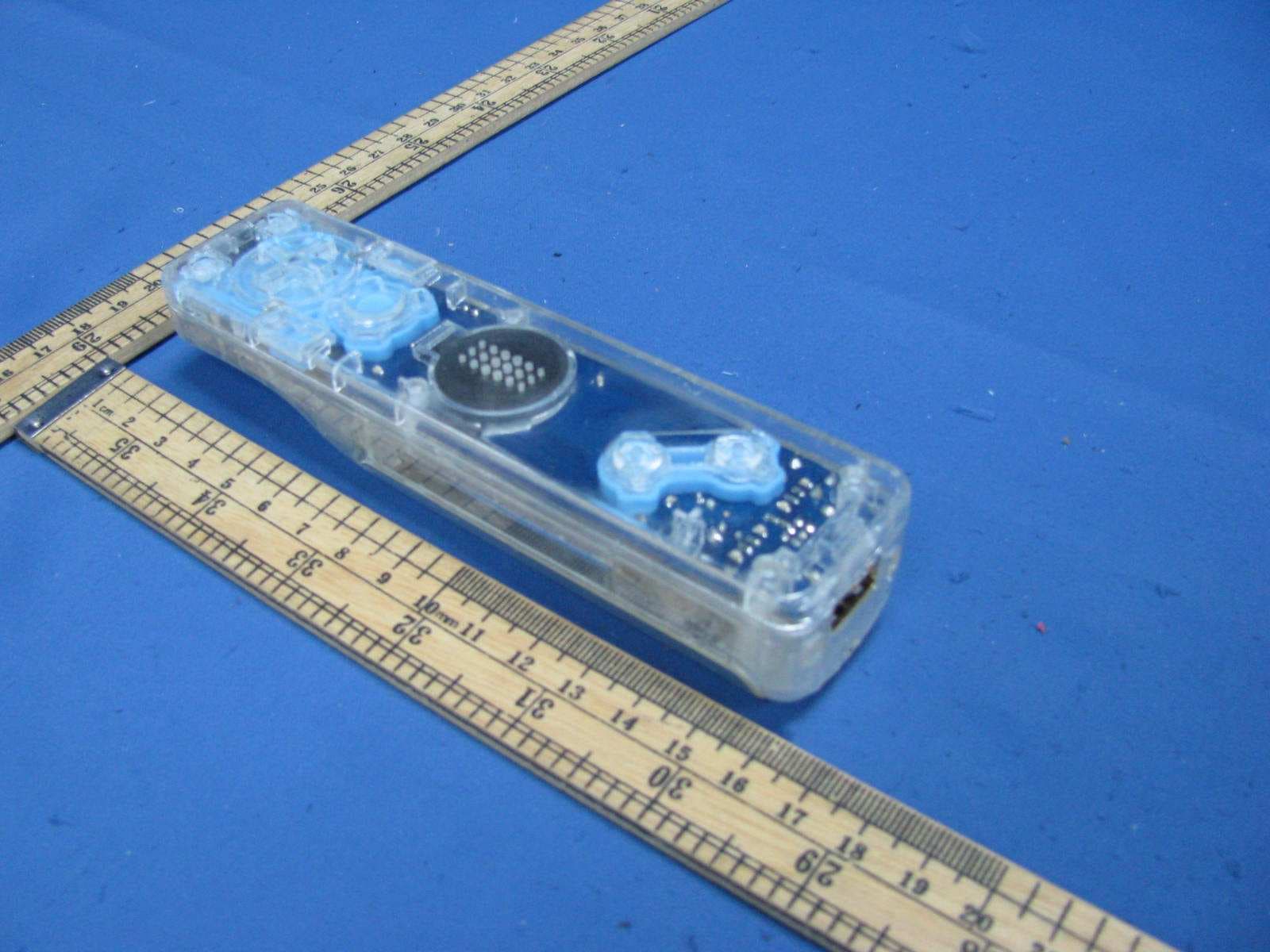
Click to zoom
Application Details
- Equipment Class
- DXX - Part 15 Low Power Communication Device Transmitter
- Date of Grant
- Mar 18, 2010
- Application Purpose
- Original Equipment
- Date of Application
- Mar 18, 2010
- Equipment Note
- Wii Remote
- Frequency Range
- 2402.00000000 - 2480.00000000
- Country
- United States
Documents & Files
Document Text
Text extracted from the exhibit documents filed with the FCC. Open a document above to read the original.
Users Manual
AFTERGLOW™ Remote For Nintendo Wii For: PL-7602 Thank you for purchasing the AFTERGLOW™ Remote for Wii® Contents: 1 AFTERGLOW™ Remote for Wii® 1 AFTERGLOW™ Remote Wrist Strap 1 Manual Using the AFTERGLOW™ Remote: 1) The AFTERGLOW™ Remote is designed to work with the Nintendo Wii® videogame system. The AFTERGLOW™ Remote must be synced to the Nintendo Wii console in order to function. 2) First, remove the battery door from the AFTERGLOW™ Remote and insert two (2) AA batteries into the compartment according to the battery orientation instructions engraved in the battery compartment. 3) Next, open the small door on the front of your Wii system. While the Wii is powered ON, press the red “Sync” button within. 4) Now, press the red “Sync” button in the AFTERGLOW™ Remote’s battery compartment. The place. 5) light. 6) Replace the battery door on the AFTERGLOW™ Remote. 7) Before play, always wear the AFTERGLOW™ Remote Wrist Strap and ensure that it is tight- ened securely around your wrist. Changing AFTERGLOW™ Modes: 1) - ATOR”, and “OFF.” 2) The green AFTERGLOW™ button in the AFTERGLOW™ Remote’s battery compartment is used to cycle through these three modes. 3) 1 1 2 2 3 4 A 1 1 2 2 3 4 1 1 2 2 3 4 CAUTION - Use the Wrist Strap - Wii gameplay with the AFTERGLOW™ Remote can involve rapid or vigorous motion. Please ensure to use the enclosed wrist strap to prevent losing your grip on the AFTERGLOW™ Remote and causing damage to the remote or surrounding objects. 1 1 2 2 3 4 HOME POWER A 4) Press the AFTERGLOW™ button once to cycle to ACCELERATOR setting. The AFTERGLOW™ Remote will vibrate twice to signal the change. In ACCELERATOR mode, AFTERGLOW™ lighting will activate when the AFTERGLOW™ Remote experiences strong acceleration. 5) Press the AFTERGLOW™ button once more. Three vibrations will signal the AFTERGLOW™ Remote is now on the OFF setting. Only the AFTERGLOW™ Remote’s appropriate player indi- cator light will glow. 6) To return to ON mode, press the AFTERGLOW™ button once more. One vibration will signal the remote is now in ON mode. 7) Cycle through the three settings as often as you like and enjoy the AFTERGLOW™ in your favorite mode! 1 1 2 2 3 4 HOME POWER A © 2010 Performance Designed Products LLC. All rights reserved. PDP and AFTERGLOW are trademarks of Performance Designed Products LLC. Wii is a registered trademark of Nintendo of America, Inc. This product is not designed, manufactured, sponsored or endorsed by Nintendo. For technical questions please visit www.pdp.com or call: 1-800-331-3844 USA ONLY *please keep this information for future reference 1840 East 27th Street Vernon, CA 90058 USA CBX II - Suite 321,382-390 Midsummer Blvd., Milton Keynes, Buckinghamshire MK9 2RG United Kingdom Waations to this unit not expressly approved by the party responsible for compliance could void the user’s authority to operate the equipment. NOTE: This equipment has been tested and found to comply with the limits for a Class B digital device, pursuant to Part 15 of the FCC Rules. These limits are designed to provide reasonable protection against harmful interference in a residential installation. This equipment generates, uses and can radiate radio frequency energy and, if not installed and used in accordance with the instructions, may cause harmful interference to radio communications. However, there is no guarantee that interference will not occur in a particular installation. If this equipment does cause harmful interference to radio or television reception, which can be ncouraged to try to correct the interference by one or more of the following measures: Reorient or relocate the receiving antenna. Increase the separation between the equipment and receiver. Connecto which the receiver is connected. Consult the dealer or an experienced radio/TV technician for help. FCC ID : X5B -PL7602 This device complies with Part 15 of the FCC Rules. Operation is subject to the following two conditions: (1) this device may not cause harmful interference, and (2) this device must accept any interference received, including interference that may cause undesired operation. IC: 8814A-PL7602 This Class B digital apparatus complies with Canadian ICES-003 Cet appareil numérique de la classe Best conforme à la norme NMB-003 du Canada.
Block Diagram
PDP Wiimote function block BT module block BT 79313 Functional Block Diagram 2.4GHz Radio RF Block Diagram
Cover Letter(s)
21 January 2010 To whom it may concern, Letter of Agency I, an officer of Performance Designed Products, LLC do hereby authorize Intertek Testing Services (Mr. Shawn Xing) to act on our behalf in front of the Federal Communications Commission with respect to all matters relating to certification of equipment under Part 15 and/or Part 95 of the FCC Rules until further notice. I further certify that no party (as defined in §1.2002(b) of CFR 47, 2007) to this application, including myself, is subject to a denial of federal benefits, that includes FCC benefits, pursuant to Section 5301 of the Anti-Drug Abuse Act of 1988, 21 U.S.C., 862. Regards, Tom Roberts Chief Technical Officer
External Photos
External Photos:
ID Label/Location Info
[March 17, 2010] To whom it may concern, Label Location Justification FCC ID: [X5B-PL7602] Request is hereby submitted by [Performance Designed Products, LLC] to request an alternative method of positively identifying the equipment, pursuant to 47 CFR § 2.925(f) of the FCC Rules. The FCC identifier for [Wii remote] will be placed in the battery compartment and the following requirements are confirmed to meet: a) The FCC identifier will visible at the time of purchase, by either of the following approaches: • Marketing the device without the battery installed, or • Providing instruction (stated on the box, user manual, or additional documentation) directing the user as to where to find the FCC label. b) The user accessible area will not require any special tools for access and the FCC label will not be placed on a removable part. The user manual has already included the FCC statements, pursuant to 47 CFR § 15.19(a)(3), 15.21 and 15.105(b). If you have questions or need further information, please contact the undersigned. Sincerely, [ Tom Roberts] [ Chief Technical Officer]
ID Label/Location Info
Label Size: 21mm*12 mm
Internal Photos
Internal Photos:
Operational Description
Technical Description The Equipment under Test (EUT) is a gamepad for the Nintendo Wii console. It is powered by a 2-AA size batteries and setup to 3.2V The main function of EUT is a gamepad included 13 keys, motion sensor, CMOS sensor, motor, sound chip, expansion port and Bluetooth module. It connects to the Wii console by Bluetooth protocol. Operating Frequency Band: 2402 MHz ~ 2480 MHz Sensitive: down to -81dBm Spread Spectrum: FHSS Modulation Method: GFSK. The functions of main ICs are mentioned as below. 1) RF1 is a Bluetooth module, including the BT79313 and EEPROM. BT79313 acts as Bluetooth Chip performs Bluetooth function, EEPROM acts as external memory. 2) U1 acts as MCU for system and gaming control. 3) U2 acts as motion sensor for gaming. 4) U7 acts as CMOS sensor module for gaming. 5) U9 acts as sound chip for gaming. 6) J1 acts as expansion port for gaming 7) Q1 acts as setup voltage regulator provide 3.2VDC to all system. BT79313 This specification are subject to be changed without notice. 2/5/2010 V1.0 - 1 - © 2009 being tech electronic corp. All rights reserved. No parts of this work may be reproduced in any form or by any means - graphic, electronic, or mechanical, including photocopying, recording, taping, or information storage and retrieval systems - without the written permission of the publisher. Products that are referred to in this document may be either trademarks and/or registered trademarks of the respective owners. The publisher and the author make no claim to these trademarks. While every precaution has been taken in the preparation of this document, the publisher and the author assume no responsibility for errors or omissions, or for damages resulting from the use of information contained in this document or from the use of programs and source code that may accompany it. In no event shall the publisher and the author be liable for any loss of profit or any other commercial damage caused or alleged to have been caused directly or indirectly by this document. Printed: December 2009 in Taiwan BT79313 Specification BT79313 This specification are subject to be changed without notice. 2/5/2010 V1.0 - 2 - General Description The BT79313 is a highly integrated single chip Bluetooth device with a stand-alone baseband processor and integrated 2.4 GHz transceiver and is compliant to Bluetooth 2.0. This chip is specifically designed for applications in wireless input devices including keyboards, mice, presenters and gaming controllers. Built-in firmware is fully compliant to Bluetooth ® Human Interface Device (HID) profile. Application − Wireless mouse − Wireless keyboard − Game controllers − Presenters − Remote controls − GPS mouse (G-mouse) RF-Transceiver − Clean, fast hopping synthesizer − 0 dBm, 1 Mbps GFSK transmitter − Analog and Digital filtered receiver − Internal VCO resonator and PLL filter − 50 ohm ant. port eliminates most external RF parts Features − Compliant with Bluetooth ® Specification V2.0 − Compliant with Bluetooth ® HID profile version 1.0 − Support AFH − Embedded 8-bits ’C51 compatible Micro-Controller − Internal 128 kB mask ROM and 8 kB SRAM − On chip support for common mouse sensor interface eliminates external processor − On chip support for Serial Peripheral Interface (SPI) (mater/slave mode) − Optional I 2 C compatible interface − Built-in Power On Reset (POR) − Built-in 8-bit accuracy/10-bit resolution ADC with 4 input channels for detecting low power of battery and reading various analog sensors such as 3-axis accelerometer, etc. − Low Power 1.8V core operation − Integrated Switch-mode Regulators (1 BUCK and 1 BOOST) to support external sensor, LED/Laser and MCU to reduce external BOM cost. − Crystal oscillator with built-in digital trimming − Power management includes digital shutdown and wake up commands with an integrated low power oscillator for sniff mode − Support MCP option with 4 Megabit Flash − Support COB (Chip on Board) option − 56-Pin QFN package available (8 x 8 x 0.9 mm) Antenna MCU ROM RAM UART 12MHz 2.4Ghz Radio Buck SPI XTAL Baseband Figure 1 – Functional Block Diagram Boost 8 bit ADC POR GPIO Batter BT79313 This specification are subject to be changed without notice. 2/5/2010 V1.0 - 3 - 1. Scope The document is a specification of BT79313. 1.1 Document Information Document No.: Version: 1.04 Total Page: 28 Date 2009/02/17 Title: ASIC Data Sheet Product Name: BT79313 1.2 Update History VersioDate/namDescription 0.0 2008/01/24 Established -- -- (status= Preliminary) 1.0 2008/12/03 Change status from Preliminary to Product. Minor updates throughou Indicate Buck regulator output as 1.83V, not 1.8V, wherever applicable. Add Key Features page. Add vendor list for xtal. Add Buck converter output filter values. 1.01 2009/02/02 Fix spelling on all page headers. Page 25: change Rr t Effective 1.02 2009/02/09 P. 1, 13, 18: Update accuracy of ADC to 8-bit. P. 3: Update T.O.C. P. 6: RF Interface: Add pin 57 to table. Clarify pins that are Test Pts. P. 10: Redraw module schematic to eliminate multiple net names. Last page: Remove leading ‘0’ from phone number. 1.03 2009/02/10 P. 5: Fix formatting of Fig. 2. Show pin 57. P. 9: Remove multiple net names on schematic. Correct spelling. P. 10: Additional schematic clean-up. Annotate photo. 1.04 2009/02/17 P. 10: Add/clarify annotations to photo. P. 16: Update Fig. 3 Bluetooth Software Stack. P. 19: Clarify first paragraph; add “optional” for Boost reg. BT79313 This specification are subject to be changed without notice. 2/5/2010 V1.0 - 4 - Key Features mCommon TX/RX terminal simplifies external matching. mFull RF reference designs available mBluetooth v2.0 Specification compliant Auxiliary Features mCrystal oscillator with built-in digital trimming mPower management includes digital shutdown and wake up commands with an integrated low power oscillator for sniff mode m8-bit ADC available with 4 input channels to applications mBuilt-in power reset to secure IC stability while powering up and t…
Text truncated - open the document above for the full version.
Schematics
1 2 34 ABCD 4 3 2 1 D CBA Title Number Revision Size A4 Date: 9-Dec-2009 Sheet of File: E:\ ៱ሽᆰໂٝ \Di sk -D\Schemati c_20 09\Wi i\Wi imot e\PDP\Wi i_PGW02 -3.dd b Drawn By: Wii_PGW02-3.Sch ( Page 1 ) RF Module D4Blue R4 680 D3Blue R3 680 D2Blue R2 680 D1Blue R1 680 C23104 12 CN1Motor ( 2222A ) R91K R7100K B 1 C 3 E 2 TR18050 Motor_ctrl R185.1R C3NC C1 8.2nH C2NC ANT CVDD GPIO0TxdRxdLED2LED3LED0 LED1 RSTnMotor_ctrlSCLKSDOSDI AMinusNC_PWRG_LEDPlus Power_keyHome CMOS_PWRSPI_CSSDOSDI SCLKnRESETSUSPEND Left Right Down UpIICDATAIICCLK TwoOneB SPI_CS C1122nF C6104 CVDD CVDD LED0LED1LED2LED3 1V8 D5D4148 CVDD NC_det4 PC6 C910uF SYNC VBAT BT1Battery VBAT C1710uF (10mil) PD3 1 PD4 2 PA2 3 VCC 4 GND 5 PA3 6 PB6 7 PB7 8 PD5 9 PD6 10 PD7 11 PB0 12 PB1 13 PB2 14 PB3 15 PB4 16 PB5 17 AVCC 18 PA0 19 PC7 20 GND 21 PA1 22 PC0 23 PC1 24 PC2 25 PC3 26 PC4 27 PC5 28 PC6 29 PD0 30 PD1 31 PD2 32 U1 BT13M880( QFN32L ) T21T22T23T24 T16 T25 T3T1T4T7T26 T5 Round T11T12 AXAY AZ T28T29T30 T35 GPIO5 (open) BT79S316 (Dice) LED1 10 GND 1 GPIO0 2 GPIO1 3 GPIO2 4 LED2 5 LED3 6 Txd_8051 7 Rxd_8051 8 LED0 9 Gnd 27 RSTn 26 HW_SELn 25 SDI 24 SDO 23 SCLK 22 GPIO7 21 Motor_ctrl 20 GPIO5 19 Power-on/off 18 Gnd 17 1V8-Out 16 Batn 11 Batp 12 VDDIO_In 13 Bst_Out 15 1V8_In 14 ANT 29 Gnd 28 Gnd 30 RF1BT79S315 NC_CVDD /0805 C510uF/0805 D11BlueD10BlueD9BlueD8BlueD7Blue R2215R CVDD R171M G_LED + C19100uF SW3 LED Key D12Blue 1 3 2 Q2 Si2301ADS G DS NC_det (option) 1 2 3 4 5 6 78 ABCD 8 7 6 5 4 3 2 1 D CBA Title Number Revision Size A3 Date: 15-Mar-2010 Sheet of File: E:\ ៱ሽᆰໂٝ \Di sk -D\Schemat ic_20 09 \Wi i\Bluet oot h Mod ule\Wi i_BT mod ule_BT79 S31 6_Di ce.dd b Drawn By: VDD-R 1 ANT 2 VDDI 3 TP 4 TN 5 AVDDA 6 VSS-ADC 7 ADC-IN0 8 VDD-ADC 9 L-Key/ADC-IN1 10 M-Key/ADC-IN2 11 P-Key/ADC-IN3 12 Z1 13 Z2 14 SCL 15 SDA 16 VSS-IO1 17 VDD-IO1 18 TXD/6-Key/SPI-SCLK 19 RXD/7-Key/SPI-SDO 20 LED0-OD 21 VDD18-C1 22 LED1-OD 23 VSS18-C1 24 Boost-BATN 25 Boost-LX 26 Boost-FB 27 Boost-BATP 28 REG-on/off 29 Buck-FB 30 Buck-BATP 31 Buck-LX 32 Buck-BATN 33 4-Key/SPI-SDI 34 5-Key/SPI-SELn 35 SHTDWN/8B-Key 36 Motion/Wkup 37 SDIO/SDA/MOSI 38 SCLK/SCL 39 VSS-IO2 41 VDD-IO2 40 MISO 42 NCS/8A-Key 43 R-Key 44 TM1 45 VDD18-C2 46 VSS18-C2 47 TM0 48 RST 49 XO 50 XI 51 VDDPL 52 DVDDA 53 VDDC 54 REGO 55 VT 56 VSS-R 57 U1 BT 79313 A0 1 A1 2 A2 3 GND 4 SDA 5 SCL 6 WP 7 VCC 8 U224LC64EEPROM R22K VDD_IO SCLSDA Battery Detector VDD_IO VBAT_P ADC_IN0 R3 560K/1% R4 560K/1% C8104 SCLBoost_FBBoost_LXSDATXD_K6RXD_K7LED0_ODLED1_OD NCS_8AKRSTnXOXIREG_Out Power_On Buck_FB Buck_LX 4_Key 5_Key SHTDWN_8BK SDIO_MOSI SCLK_SCL MISO ANT ADC_IN0 L_Key M_Key P_Key Z1 Z2 E1 ANTENNA IN 4 OUT 2 GND 1 GND 3 FL1 MDR774M-T C11NC C12NC C10 0R CP1 1uF CP21uF VCC_1V8 AVDDA AVDDA VCC_1V8 1V8_In Boost_BATN Buck_BATN Boost_BATNBuck_BATN VBAT_P Boost_BATPBuck_BATP VBAT_P Boost_BATP Buck_BATP VBAT_P C4 4.7uF R50R VDD_IO1 VDD_IO2 VDD_IO1VDD_IO2 VDD_IO VDD_IO VSS_IO1VSS18_C1 CP12 1uF CP111uF P12 VSS_IO2 VBAT_N VSS_ADC VSS18_C2 P13 CP34.7uF VCC_1V8 VDDPL CP41uF DVDDAVDDC CP54.7uF VDDR CP6 4.7uF VCC_1V8 VDD18_C1 CP81uF VCC_1V8 VDD18_C2 VCC_1V8 CP91uF Y112M XOXI R11M C5 27P C6 27P CLOCK P3 P4 P5 P6 P7 P8P9P10P11 P14P16 L1 SDN2624-100M Buck_FBBuck_LX C14.7uF Buck_Out P17 Internal Boost & Buck VBAT_P Boost_BATP L2 SDN2624-4R7K Boost_FB C34.7uF Boost_OutBoost_LX P15 C24.7uF C3 will be closed to L2 Power of NetsVBAT_N P1 P18 P19 P20 P21 P22 P24 P25 P26 P27 P29 P30 VSS_F VCC_1V8 CP10 1uF VDD_ADC (open) (open) (open) (DICE) Wii_BT module_BT79S316-5 (Dice).Sch TSSOP-8 10ppm 10uH (open) (open) (open) (open) (open) (open) (open) 1 2 34 ABCD 4 3 2 1 D CBA Title Number Revision Size A4 Date: 9-Dec-2009 Sheet of File: E:\ ៱ሽᆰໂٝ \Di sk -D\Schemati c_20 09\Wi i\Wi imot e\PDP\Wi i_PGW02 -3.dd b Drawn By: Wii_PGW02-3.Sch ( Page 2 ) S1 Left S6 ONE S10 Plus S2 Right S7BS4UpS3 Down S8A S9 Minus S11 Home S5 TWO Key *13ADownRightLeftBOneTwo Home Up PlusMinus SW1 SYNC SW2 POWER SYNC POWER_key 123456 J1I2C Conn Interface R6100K IICDATAIICCLK NC_det G-Sensor R19 6.8K NC_CVDD IICDATAIICCLK 1 3 2 Q3 Si2301ADS R51M + C33100uF G DS R21 6.8K IICDATAIICCLK NC_CVDD CVDD Power Section NC_CVDD GPIO 1 VSS 2 SCL 3 VDD 4 SDA 5 EXTCLK 6 NC 7 RST 8 U7BT47S200 T13 T14 T9T10 T15 T27 T17T18T19 T20 NC_CVDD CMOS_PWR NC_PWR R1010K NC 1 NC 2 NC 3 GND 4 VDD 5 IOEF0 6 IOAB0 7 RESETB 8 VSS 9 AVSS2 10 AUDPL 11 AVDD 12 AUDPR 13 AVSS1 14 VM 15 LFC 16 U9BT52R310 NC_CVDD AUDPRAUDPL SP1 SPEAKER C8 104 C722uF NC_CVDD C4 104 nRESETSUSPEND C16 22nF ON/OFF 1 VOUT 2 NC 3 VSS 4 CONT 5 Q1 FP6731 VBAT CVDD D6 SL24 C10104 C13104 C14104 C15104 AXAYAZ T34T33 L1 2.2uH T32 (SSOP16 / SOP16) + C21 E/C, 100uF C2010uF R13 10K C182.2uF C2222uF /0805 /0805 (open) SOT-23-5 (open) 5*11mm C16 depend on Sound( 47nF ) /0805 (open) NC 1 ST 2 COM 3 NC 4 COM 5 COM 6 COM 7 Zout 8 NC 9 Yout 10 NC 11 Xout 12 NC 13 VS 14 VS 15 NC 16 U2ADXL335 C12 104 GPIO5 + C24 470uF/10V E/C, 8*7mm R8 100K
Test Report
Packet DH1: Ref 87 dBμVAtt 0 dB ** A TDF 1 MHz/Center 2.4 GHzSpan 10 MHz * * 3DB RBW 100 kHz VBW 300 kHz SWT 200 ms * 1 PK VIEW -10 0 10 20 30 40 50 60 70 80 1 Marker 1 [T1 ] 69.56 dBμV 2.401997000 GHz 2 Marker 2 [T1 ] 16.76 dBμV 2.400020000 GHz Ref 87 dBμVAtt 0 dB ** A TDF 1 MHz/Center 2.4835 GHzSpan 10 MHz * * 3DB RBW 100 kHz VBW 300 kHz SWT 200 ms * 1 PK VIEW -10 0 10 20 30 40 50 60 70 80 1 Marker 1 [T1 ] 66.93 dBμV 2.480140000 GHz 2 Delta 2 [T1 ] -51.41 dB 3.400000000 MHz
Test Report
Packet DH5: Ref 87 dBμVAtt 0 dB ** A TDF Center 2.402 GHzSpan 3 MHz300 kHz/ * 3DB RBW 100 kHz SWT 200 ms * VBW 300 kHz * 1 PK VIEW -10 0 10 20 30 40 50 60 70 80 1 Marker 1 [T1 ] 64.98 dBμV 2.402054000 GHz ndB [T1] 20.00 dB BW 1.122000000 MHz T1 Temp 1 [T1 ndB] 45.07 dBμV 2.401430000 GHz T2 Temp 2 [T1 ndB] 44.64 dBμV 2.402552000 GHz Ref 87 dBμVAtt 0 dB ** A TDF Center 2.441 GHzSpan 3 MHz300 kHz/ 3DB SWT 200 ms * * * RBW 100 kHz VBW 300 kHz 1 PK VIEW -10 0 10 20 30 40 50 60 70 80 1 Marker 1 [T1 ] 66.19 dBμV 2.441138000 GHz ndB [T1] 20.00 dB BW 1.140000000 MHz T1 Temp 1 [T1 ndB] 46.13 dBμV 2.440418000 GHz T2 Temp 2 [T1 ndB] 46.23 dBμV 2.441558000 GHz Date: 23.DEC.2009 09:35:21 Ref 87 dBμVAtt 0 dB ** A TDF Center 2.48 GHzSpan 3 MHz300 kHz/ 3DB SWT 200 ms * * * RBW 100 kHz VBW 300 kHz 1 PK VIEW -10 0 10 20 30 40 50 60 70 80 1 Marker 1 [T1 ] 65.33 dBμV 2.480144000 GHz ndB [T1] 20.00 dB BW 1.188000000 MHz T1 Temp 1 [T1 ndB] 45.09 dBμV 2.479406000 GHz T2 Temp 2 [T1 ndB] 45.17 dBμV 2.480594000 GHz Date: 23.DEC.2009 09:39:11
Test Report
Intertek Testing Services Shenzhen Ltd. Kejiyuan Branch 6F, D Block, Huahan Building, Langshan Road, Nanshan District, Shenzhen, P. R. China Tel: (86 755) 8601 6288 Fax: (86 755) 8601 6751 Website: www.china.intertek-etlsemko.com February 20, 2010 Performance Designed Products, LLC 14144 Ventura Blvd, Suite 200 Sherman Oaks CA, 91423 United States Dear Tom Roberts : Enclosed you will find your file copy of a Part 15 Certification (FCC ID: X5B-PL7602). For your reference, TCB will normally take another 5-10 workdays for reviewing the report. Approval will then be granted when no query is sorted. Please contact me if you have any questions regarding the enclosed material. Sincerely, Shawn Xing Assistant Manager Enclosure • The test results reported in this test report shall refer only to the sample actually tested and shall not refer or be deemed to refer to bulk from which such a sample may be said to have been obtained. • This report is for the exclusive use of Intertek's Client and is provided pursuant to the agreement between Intertek and its Client. Intertek's responsibility and liability are limited to the terms and conditions of the agreement. Intertek assumes no liability to any party, other than to the Client in accordance with the agreement, for any loss, expense or damage occasioned by the use of this report. Only the Client is authorized to copy or distribute this report. Any use of the Intertek name or one of its marks for the sale or advertisement of the tested material, product or service must first be approved in writing by Intertek. The observations and test results referenced from this report are relevant only to the sample tested. This report by itself does not imply that the material, product, or service is or has ever been under an Intertek certification program. • For Terms And Conditions of the services, it can be provided upon request. • The evaluation data of the report will be kept for 3 years from the date of issuance. TRF No.: FCC 15C_TXa FCC ID: X5B-PL7602 Intertek Testing Services Shenzhen Ltd. Kejiyuan Branch 6F, D Block, Huahan Building, Langshan Road, Nanshan District, Shenzhen, P. R. China Tel: (86 755) 8601 6288 Fax: (86 755) 8601 6751 Website: www.china.intertek-etlsemko.com Performance Designed Products, LLC Application For Certification (FCC ID: X5B-PL7602) Wii remote MODEL: PL7602 2.4GHz Transceiver SZ09120239-1 Billy Li February 20, 2010 INTERTEK TESTING SERVICES TRF No.: FCC 15C_TXa FCC ID: X5B-PL7602 i LIST OF EXHIBITS INTRODUCTION EXHIBIT 1: General Description EXHIBIT 2: System Test Configuration EXHIBIT 3: Emission Results EXHIBIT 4: Equipment Photographs EXHIBIT 5: Product Labelling EXHIBIT 6: Technical Specifications EXHIBIT 7: Instruction Manual EXHIBIT 8: Miscellaneous Information EXHIBIT 9: Test Equipment List INTERTEK TESTING SERVICES TRF No.: FCC 15C_TXa FCC ID: X5B-PL7602 ii MEASUREMENT/TECHNICAL REPORT Performance Designed Products, LLC - MODEL: PL7602 FCC ID: X5B-PL7602 February 20, 2010 This report concerns (check one:) Original Grant X Class II Change Equipment Type: DXX - Part 15 Low Power Communication Device Transmitter Deferred grant requested per 47 CFR 0.457(d)(1)(ii)? Yes No X If yes, defer until: date Company Name agrees to notify the Commission by: date of the intended date of announcement of the product so that the grant can be issued on that date. Transition Rules Request per 15.37? Yes No X If no, assumed Part 15, Subpart C for intentional radiator − the new 47 CFR [10-1-08 Edition] provision. Report prepared by: Shawn Xing Intertek Testing Services Shenzhen Ltd. Kejiyuan Branch 6F, Block D, Huahan Building, Langshan Road, Nanshan District, Shenzhen, P. R. China Phone: (86 755) 8601 6288 Fax: (86 755) 8601 6751 INTERTEK TESTING SERVICES TRF No.: FCC 15C_TXa FCC ID: X5B-PL7602 iii Table of Contents 1.0 General Description............................................................................................ 2 1.1 Product Description ............................................................................................ 2 1.2 Related Submittal(s) Grants ............................................................................... 2 1.3 Test Methodology............................................................................................... 3 1.4 Test Facility........................................................................................................ 3 2.0 System Test Configuration ................................................................................. 5 2.1 Justification ........................................................................................................ 5 2.2 EUT Exercising Software.................................................................................... 5 2.3 Special Accessories ........................................................................................... 5 2.4 Equipment Modification ...................................................................................... 5 2.5 Measurement Uncertainty .................................................................................. 6 2.6 Support Equipment List and Description ............................................................. 6 3.0 Emission Results................................................................................................ 8 3.1 Field Strength Calculation................................................................................... 9 3.2 Radiated Emission Configuration Photograph................................................... 10 3.3 Radiated Emission Data ................................................................................... 11 4.0 Equipment Photographs................................................................................... 17 5.0 Product Labelling .............................................................................................. 19 6.0 Technical Specifications........................................................…
Text truncated - open the document above for the full version.
Test Setup Photos
Radiated Photos:
Contact Information
Applicant
Tom Roberts(Chief Technical Officer)
Technical Contact
Intertek Testing Services Shenzhen Ltd KejiyuanShawn Xing
[email protected]8675586140603
6F, D Block, Huahan Building, Langshan Road · Shenzhen · China
Non-Technical Contact
Intertek Testing Services Shenzhen Ltd KejiyuanShawn Xing
[email protected]8675586140603
Test Firm
Intertek Testing Services Shenzhen Ltd.Shawn Xing
Technical Specifications
| # | Rule Parts | Frequency Range | Power Output |
|---|---|---|---|
| 1 | 15C | 2.40 GHz - 2.48 GHz | - |
Other Applications from Performance Designed Products, LLC
X5B-049037X
Aug 22, 2024PDP REALMz Wireless Controller for Xbox
Equipment Class
DTS - Digital Transmission SystemX5B-049037T
Aug 22, 2024PDP REALMz Wireless Dongle for Xbox
Equipment Class
DTS - Digital Transmission SystemX5B-500253
Aug 02, 2024Rematch Wireless Controller for Nintendo Switch
Equipment Class
DSS - Part 15 Spread Spectrum TransmitterX5B-500246
Aug 01, 2024Wireless Controller for Nintendo Switch
Equipment Class
DSS - Part 15 Spread Spectrum TransmitterX5B-049038X
Jun 28, 2024Phantom Air Wireless Headset for Xbox / Phantom Air Wireless Headset for Play Station
Equipment Class
DSS - Part 15 Spread Spectrum Transmitter