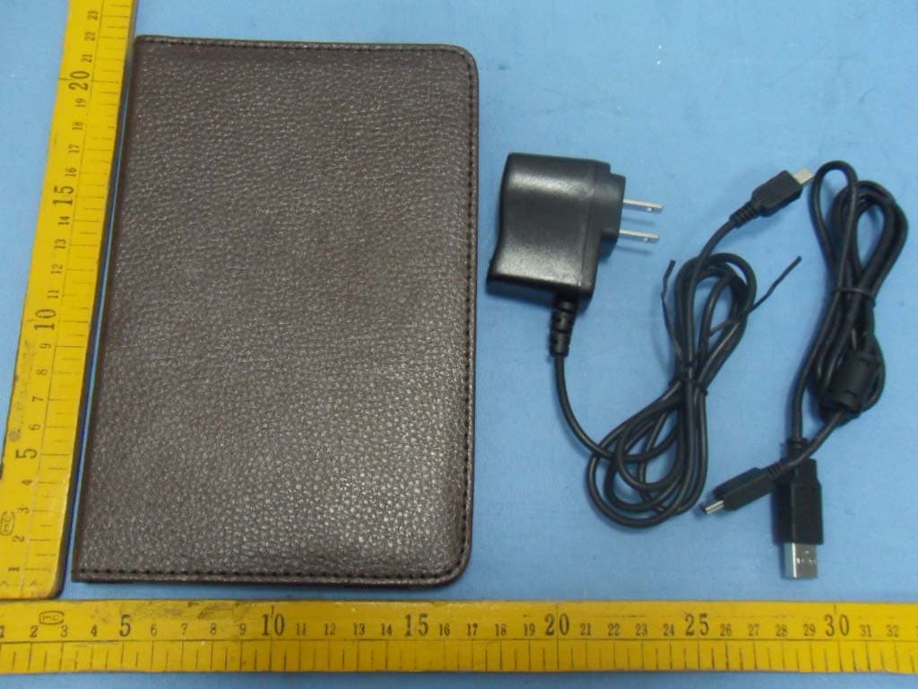
Click to zoom
Application Details
- Equipment Class
- JBP - Part 15 Class B Computing Device Peripheral
- Date of Grant
- Jun 23, 2010
- Application Purpose
- Original Equipment
- Date of Application
- Jun 23, 2010
- Equipment Note
- E-BOOK
- Country
- China
Documents & Files
Document Text
Text extracted from the exhibit documents filed with the FCC. Open a document above to read the original.
Users Manual
Home Menu Shelf Management Quick Find Entertainment T X T E P U B P D F C B A Continue Reading Settings By TitleBy AuthorBy format Recent Read Power offRecent Bookmarks My Favorites AudioPicturesGames B o o k m a r k Thanks for purchasing our product. Please read this manual carefully before starting to use this device. 1. Key Introduction 2. Function Introduction Top Bottom FrontBack Power On/Off Reset SD Card Slot Enter Key (You can click here to adjust the font size) Bookmark (You can click here to add bookmarks when reading) Rotate (You can click here to switch display mode when reading) Indicator Screen Battery Cap Previous Next Menu Return Direction Key Mini-USB Slot 2.5mm Earphone Slot Power On: In power off status, press the power button to turn on the device, then the “boot screen” will be displayed on screen. Power Off In power-on mode, press the power button on the device or select the “Power Off ” sign on the UI to shutdown the device. 2.1 Power On/Off 2.2 System UI After power on, under this UI, click icon on the screen to enter the function page. By Title: Sort articles by title By Author: Sort articles by author By Format: Sort articles by format Continue Read: Continue read the article you read recently Recent Read: Articles list you read recently My Favorite: Your favourite articles Music: Listening music Picture: Viewing pictures Games: Playing games Recent Bookmarks: Recent bookmarks you set Power Off: Shutdown the machine Settings: Setting the machine parameters 3. Charger Application Take out the USB charger, plug it into the wall outlet with AC 100V~240V, then plug the USB jack into the device. (see the illustration below). 4. Note 5. FCC NOTE Security: Do not use the device while driving. Display: Please do not squeeze and hit this equipment may cause injury. THE MANUFACTURER IS NOT RESPONSIBLE FOR ANY RADIO OR TV INTERFERENCE CAUSED BY UNAUTHORIZED MODIFICATIONS TO THIS EQUIPMENT. SUCH MODIFICATIONS COULD VOID THE USER’S AUTHORITY TO OPERATE THE EQUIPMENT. This device complies with Part 15 of the FCC Rules. Operation is subject to the following two conditions: 1. This device may not cause harmful interference, and 2. This device must accept any interference received, including interference that may cause undesired operation. 万册书百万字容量 纳 容 大 EB602 USB jack 1234 size:100x160mm 2010.06.11 V1.0 Qucik User Guide 物料名称:EB602简易说明书 NOTE: This equipment has been tested and found to comply with the limits for a Class B digital device, pursuant to Part 15 of the FCC Rules. These limits are designed to provide reasonable protection against harmful interference in a residential installation. This equipment generates, uses and can radiate radio frequency energy and, if not installed and used in accordance with the instructions, may cause harmful interference to radio communications. However, there is no guarantee that interference will not occur in a particular installation. If this equipment does cause harmful interference to radio or television reception, which can be determined by turning the equipment off and on, the user is encouraged to try to correct the interference by one or more of the following measures: —Reorient or relocate the receiving antenna. —Increase the separation between the equipment and receiver. —Connect the equipment into an outlet on a circuit different from that to which the receiver is connected. —Consult the dealer or an experienced radio/TV technician for help.
Block Diagram
EB602 Hardware Block Diagram V.3.3 PVI E-ink LCD Panel V Driver(Gate) LCD Panel N Driver(Source) Source Driver Gate Driver Control Signals VGH VGL NOR Flash 8M SRA M 128K *2 EPD Timming control PVI6001 A PVI6001A HOST Interface DC-DC Panel Power Cl VMAX NAND Flash 1G DDR1 64mx2 ARM11 S3C6410 Power management Battery Audio Codec 11 Fun. Keys USB SW USB DC IN VBUS IN V3.3 V1.3 REST Power Ctrl USB Mini AB Receptacle SD Socket Address BUS Data BUS Address BUS Data BUS SD Host USB Device USB Host Address BUS Data BUS IIS Interface Headhone jack Crustal 12MHz
External Photos
FCC ID: XAJEB602 Page 25 o f 29 Anbotek Compliance Laboratory Limited Report No. 201006724F Figure 1 The EUT-Overall View Figure 2 The EUT-Front View FCC ID: XAJEB602 Page 26 o f 29 Anbotek Compliance Laboratory Limited Report No. 201006724F Figure 3 The EUT-Front View Figure 4 The EUT-Back View
ID Label/Location Info
FCC ID Label Sample for FCC ID:EB602
ID Label/Location Info
The proposed Label Location on EUT Proposed FCC ID Label Location Proposed Label Location on EUT The EUT-Back View/Proposed FCC ID Label Location
Internal Photos
FCC ID: XAJEB602 Page 27 o f 29 Anbotek Compliance Laboratory Limited Report No. 201006724F Figure 5 The EUT-Inside View Figure 6 The EUT-Inside View FCC ID: XAJEB602 Page 28 o f 29 Anbotek Compliance Laboratory Limited Report No. 201006724F Figure 7 PCB of the EUT-Front View Figure 8 PCB of the EUT-Back View FCC ID: XAJEB602 Page 29 o f 29 Anbotek Compliance Laboratory Limited Report No. 201006724F Figure 9 PCB of the EUT-Front View Figure 10 PCB of the EUT-Back View
Operational Description
EB602 Circuit Description EB602 uses SAMSUNG s3c6410 ARM1176JZF-S 667MHZ Support 6” E_ink, 800x600 pixels, 64MBx2 DDRI, 1GB Nand flash memory, Expandable via SD card (up to 4GB). 1. The Power management IC TPS650243 Supply DC3.3V/2.5V/1.2V a set of voltage to support system. 2. Chipset IC SAMSUNG s3c6410(ARM11),connect to nand flash or DDR1 memory through Address BUS and Data BUS. It control Audio codec (WM9751LG) through IIS. 3. Chipset IC SAMSUNG s3c6410 ARM11), connect to SD Socket /keys/USB 4. Chipset IC PVI (PVI6001A),connect to NOR Flash or SRAM through Address BUS and Data BUS, the same time control 6” LCD panel display. 5. Chipset IC PVI (PVI6001A),connect to CPU s3c6410 through HOST Interface.
Schematics
5 5 4 4 3 3 2 2 1 1 DD CC BB AA Xm1ADDR12 Xm1ADDR11 Xm1ADDR10 Xm1ADDR9 Xm1ADDR8 Xm1ADDR7 Xm1ADDR6 Xm1ADDR5 Xm1ADDR4 Xm1ADDR3 Xm1ADDR2 Xm1ADDR1 Xm1ADDR0 X m 1 D A T A 3 1 X m 1 D A T A 3 0 X m 1 D A T A 2 9 X m 1 D A T A 2 8 X m 1 D A T A 2 7 X m 1 D A T A 2 6 Xm0DATA0 Xm0DATA1 Xm0DATA2 X m 1 D A T A 2 5 X m 1 D A T A 2 4 X m 1 D A T A 2 3 Xm0DATA3 Xm0DATA4 Xm0DATA5 Xm0DATA6 Xm0DATA7 Xm0DATA8 Xm0DATA9 X m 1 D A T A 2 2 X m 1 D A T A 2 1 X m 1 D A T A 2 0 Xm0DATA10 Xm0DATA11 Xm0DATA12 Xm0DATA13 Xm0DATA14 Xm0DATA15 X m 1 D A T A 1 9 X m 1 D A T A 1 8 X m 1 D A T A 1 7 X m 1 D A T A 1 6 X m 1 D A T A 1 5 X m 1 D A T A 1 4 X m 1 D A T A 1 3 X m 1 D A T A 1 2 X m 1 D A T A 1 1 X m 1 D A T A 1 0 X m 1 D A T A 9 X m 1 D A T A 8 X m 1 D A T A 7 X m 1 D A T A 6 X m 1 D A T A 5 X m 1 D A T A 4 X m 1 D A T A 3 X m 1 D A T A 2 X m 1 D A T A 1 X m 1 D A T A 0 Xm1ADDR15 Xm1ADDR14 Xm0WEn/nIOWR_CF6,9 Xm1DQS35 Xm1DQS25 Xm1DQS15 Xm1DQS05 Xm1DQM35 Xm1DQM25 Xm0CSn06 Xm1DQM15 Xm1DQM05 Xm0CSn1 Xm1WEn5 Xm1CASn5 Xm1RASn5 Xm1SCLKn5 Xm1SCLK5 Xm0CSn26 Xm1CKE05 Xm0CSn5 Xm0CSn36 Xm0CSn7 Xm0RDY0/ALE6 Xm0CSn6 Xm0RDY1/CLE6 Xm0INTsm0/FWEn6 Xm0INTsm1/FREn6 Xm0RPn/RnB6 Xm1DATA[31:0] 5 Xm0DATA[15:0]6 Xm0WAITn/IORDY Xm0INTata Xm0INPACKata Xm0CData Xm0RSTata Xm0REGata Xm0WEata Xm0OEata Xm1ADDR[12:0]5 Xm1CSn15 Xm0OEn/nIORD_CF6,9 Xm1CSn05 Xm0CSn1 Xm0CSn5 Xm0CSn7 Xm0CSn6 Xm0WAITn/IORDY Xm0INTata Xm0INPACKata Xm0CData Xm0RSTata Xm0REGata Xm0WEata Xm0OEata Xm1ADDR155 Xm1ADDR145 Xm1CKE15 Xm0ADDR29 Title SizeDocument NumberRev Date:Sheetof CPU(Data , Addr)<ver1.0 EB602 MAIN PART A3 111Thursday, November 12, 2009 Title SizeDocument NumberRev Date:Sheetof CPU(Data , Addr)<ver1.0 EB602 MAIN PART A3 111Thursday, November 12, 2009 Title SizeDocument NumberRev Date:Sheetof CPU(Data , Addr)<ver1.0 EB602 MAIN PART A3 111Thursday, November 12, 2009 TP7TP7 TP11TP11 TP4TP4 TP1TP1 TP2TP2 HOLE2HOLE2 HOLE1HOLE1 TP8TP8 TP9TP9 TP5TP5 U1A S3C6410 U1A S3C6410 Xm0ADDR0 C1 Xm0ADDR1 E3 Xm0ADDR2 D1 Xm0ADDR3 D2 Xm0ADDR4 H7 Xm0ADDR5 E1 Xm0ADDR6/GPO6 F2 Xm0ADDR7/GPO7 G4 Xm0ADDR8/GPO8 F1 Xm0ADDR9/GPO9 J8 Xm0ADDR10/GPO10 G2 Xm0ADDR11/GPO11 G1 Xm0ADDR12/GPO12 H4 Xm0ADDR13/GPO13 H2 Xm0ADDR14/GPO14 J4 Xm0ADDR15/GPO15 H3 Xm0DATA0 N2 Xm0DATA1 N1 Xm0DATA2 M7 Xm0DATA3 N3 Xm0DATA4 M8 Xm0DATA5 P2 Xm0DATA6 N4 Xm0DATA7 P3 Xm0DATA8 M2 Xm0DATA9 M4 Xm0DATA10 L7 Xm0DATA11 M3 Xm0DATA12 L8 Xm0DATA13 L2 Xm0DATA14 K4 Xm0DATA15 K1 Xm0OEn/nIORD_CF L4 Xm0WEn/nIOWR_CF J2 Xm0ADV/GPP0 Y2 Xm0SMCLK/GPP1 L3 X m 0 C S n 0 N 7 X m 0 C S n 1 R 3 X m 0 C S n 2 / G P O 0 P 4 X m 0 C S n 3 / G P O 1 R 2 X m 0 C S n 4 / G P O 2 T 3 X m 0 C S n 5 / G P O 3 N 8 X m 0 C S n 6 / G P O 4 T 2 X m 0 C S n 7 / G P O 5 P 7 X m 0 W A I T n / I O R D Y / G P P 2 R 4 X m 0 R D Y 0 / A L E / G P P 3 R 8 X m 0 R D Y 1 / C L E / G P P 4 W 2 X m 0 I N T s m 0 / F W E n / G P P 5 Y 3 X m 0 I N T s m 1 / F R E n / G P P 6 U 4 X m 0 R P n / R n B / G P P 7 Y 1 X m 0 I N T a t a / G P P 8 R 7 X m 0 R S T a t a / G P P 9 W 3 X m 0 I N P A C K a t a / G P P 1 0 A A 2 X m 0 R E G a t a / G P P 1 1 A A 3 X m 0 W E a t a / G P P 1 2 V 4 X m 0 O E a t a / G P P 1 3 A B 3 X m 0 C D a t a / G P P 1 4 U 7 X m 0 D Q M 0 / B E 0 L 1 X m 0 D Q M 1 / B E 1 K 7 X m 0 R A S / G P Q 0 U 2 X m 0 C A S / G P Q 1 P 8 X m 0 S C L K / G P Q 2 T 1 X m 0 S C L K n / G P Q 3 U 1 X m 0 C K E / G P Q 4 V 3 X m 0 D Q S 0 / G P Q 5 T 4 X m 0 D Q S 1 / G P Q 6 V 2 X m 0 W E n d m c / G P Q 7 U 3 X m 0 A P d m c / G P Q 8 J 1 Xm1CKE0 M18 Xm1CKE1 M24 Xm1SCLK A13 Xm1SCLKn A14 Xm1RASn L22 Xm1CASn L24 Xm1WEn M19 Xm1DQM0 A5 Xm1DQM1 G8 Xm1DQM2 D14 Xm1DQM3 H22 Xm1DQS0 D9 Xm1DQS1 G9 Xm1DQS2 B14 Xm1DQS3 E25 Xm1CSn0 L23 Xm1CSn1 L18 Xm1ADDR0 H24 Xm1ADDR1 J24 Xm1ADDR2 J23 Xm1ADDR3 H25 Xm1ADDR4 L19 Xm1ADDR5 K25 Xm1ADDR6 J25 Xm1ADDR7 K18 Xm1ADDR8 K23 Xm1ADDR9 J22 Xm1ADDR10 M23 Xm1ADDR11 K19 Xm1ADDR12 K24 Xm1ADDR13 K22 Xm1ADDR14 M17 Xm1ADDR15 L25 X m 1 D A T A 0 B 6 X m 1 D A T A 1 A 6 X m 1 D A T A 2 C 7 X m 1 D A T A 3 B 7 X m 1 D A T A 4 C 6 X m 1 D A T A 5 C 8 X m 1 D A T A 6 A 9 X m 1 D A T A 7 C 9 X m 1 D A T A 8 D 1 2 X m 1 D A T A 9 A 1 0 X m 1 D A T A 1 0 C 1 2 X m 1 D A T A 1 1 D 1 1 X m 1 D A T A 1 2 A 1 1 X m 1 D A T A 1 3 B 1 0 X m 1 D A T A 1 4 C 1 1 X m 1 D A T A 1 5 D 1 0 X m 1 D A T A 1 6 / X m 0 A D D R 1 6 B 1 2 X m 1 D A T A 1 7 / X m 0 A D D R 1 7 B 1 3 X m 1 D A T A 1 8 / X m 0 A D D R 1 8 A 1 2 X m 1 D A T A 1 9 / X m 0 A D D R 1 9 C 1 3 X m 1 D A T A 2 0 / X m 0 A D D R 2 0 C 1 5 X m 1 D A T A 2 1 / X m 0 A D D R 2 1 D 1 5 X m 1 D A T A 2 2 / X m 0 A D D R 2 2 B 1 5 X m 1 D A T A 2 3 / X m 0 A D D R 2 3 D 1 6 X m 1 D A T A 2 4 / X m 0 A D D R 2 4 F 2 3 X m 1 D A T A 2 5 / X m 0 A D D R 2 5 F 2 4 X m 1 D A T A 2 6 / X m 0 A D D R 2 6 F 2 5 X m 1 D A T A 2 7 G 2 4 X m 1 D A T A 2 8 E 2 4 X m 1 D A T A 2 9 G 2 3 X m 1 D A T A 3 0 G 2 5 X m 1 D A T A 3 1 H 2 3 TP6TP6 TP10TP10 TP12TP12 TP48TP48 TP3TP3 Create PDF with GO2PDF for free, if you wish to remove this line, click here to buy Virtual PDF Printer 5 5 4 4 3 3 2 2 1 1 DD CC BB AA XEINT4 XREXT Z_SCL Z_SDA XotgTI XEXTCLK XEINT4 VDD_D VDD_D VDD_D VDD_D VDD_D VDD_D VDD_D XnRESET 6 XSELNAND6 XnRESET6 XPWRRGTON10 XOM46 XOM36 XOM26 XOM16 XOM06 XDBGSEL6 XTDI9 XTCK9 XTMS9 XTRSTn9 XRTCK9 XTDO9 XuRXD_09 XuRXD_19 XuTXD_09 XuTXD_19 Xi2cSCL2 Xi2cSDA2 XotgTO6 XVBUS9 10 XEINT7/KP_ROW710 XEINT1110 XEINT132,11 XEINT152 XXTI6 X27MXTI6 XrtcXTI6 XmmcCLK0/ADDR_CF09 XXTO6 XmmcCMD0/ADDR_CF19 XmmcDATA0_0/ADDR_CF29 XmmcDATA0_19 XmmcDATA0_29 XmmcDATA0_39 X27MXTO6 XmmcDATA1_7/mmcDATA2_39 XPCM_DCLK0/I2S_CLK0/AC97_BITCLK0/ADDR_CF07 XPCM_EXTCLK0/I2S_CDCLK0/AC97_RSTn0/ADDR_CF17 XPCM_FSYNC0/I2S_LRCLK0/AC97_SYNC0/ADDR_CF27 XPCM_SOUT0/I2S_DO0/AC97_SDO07 XrtcXTO6 XmmcCDN0/mmcCDN19 XPCM_SIN0/I2S_DI0/AC97_SDI07 Xi2cSDA2 Xi2cSCL2 XotgTI6 GPN08 LAN_INT 9 XnRSTOUT 9 XotgID9 XEINT132 XEINT152 XEINT142 XEINT142 XEINT310 XEINT510 XotgDP9 XotgDM9 Title SizeDocument NumberRev Date:Sheetof CPU( I/O)ver1.0 EB602 MAIN PART A3 211Wednesday, June 09, 2010 Title SizeDocument NumberRev Date:Sheetof CPU( I/O)ver1.0 EB602 MAIN PART A3 21…
Text truncated - open the document above for the full version.
Test Report
FCC ID: XAJEB602 Page 1 o f 29 Anbotek Compliance Laboratory Limited Report No. 201006724F FCC TEST REPORT FOR Matsunichi Communication Holdings R&D (Shenzhen) Co., Ltd. E-BOOK Model No.: EB602 Prepared for : Matsunichi Communication Holdings R&D (Shenzhen) Co., Ltd. Address : 43B/F, INTERNAL CHAMBER OF COMMERCE TOWER, FUHUA RD3 CBD, FUTIAN DISTRICT, SHENZHEN, CHINA Tel: (86) 755-88315408 Fax: (86) 755-88313194 Prepared By : Anbotek Compliance Laboratory Limited Address : 2F, Langfeng Building, Kefa Road North, Hi-tech Industrial Park, Nanshan District, Shenzhen 518057, China Tel: (86) 755-26014771 Fax: (86) 755-26014772 Report Number : 201006724F Date of Test : Jun. 13~23, 2010 Date of Report : Jun. 24, 2010 FCC ID: XAJEB602 Page 2 o f 29 Anbotek Compliance Laboratory Limited Report No. 201006724F TABLE OF CONTENTS Description Page Test Report Verification 1. GENERAL INFORMATION ............................................................................................................... 4 1.1. Description of Device (EUT) ..........................................................................................................................4 1.2. Description of Test Facility.............................................................................................................................5 1.3. Measurement Uncertainty ...............................................................................................................................5 2. POWER LINE CONDUCTED MEASUREMENT ............................................................................ 6 2.1. Test Equipment ...............................................................................................................................................6 2.2. Block Diagram of Test Setup ..........................................................................................................................6 2.3. Power Line Conducted Emission Measurement Limits (FCC Part 15 Class B) .............................................6 2.4. Configuration of EUT on Measurement..........................................................................................................7 2.5. Operating Condition of EUT...........................................................................................................................7 2.6. Test Procedure.................................................................................................................................................7 2.7. Power Line Conducted Emission Measurement Results.................................................................................7 3. RADIATED EMISSION MEASUREMENT..................................................................................... 12 3.1. Test Equipment .............................................................................................................................................12 3.2. Block Diagram of Test Setup ........................................................................................................................12 3.3. Radiated Emission Limit (Subpart B Class B) ..............................................................................................13 3.4. EUT Configuration on Measurement ............................................................................................................13 3.5. Operating Condition of EUT.........................................................................................................................13 3.6. Test Procedure...............................................................................................................................................14 3.7. Radiated Emission Measurement Results .....................................................................................................14 4. PHOTOGRAPH ................................................................................................................................... 21 4.1. Photo of Power Line Conducted Emission Test............................................................................................21 4.2. Photo of Radiated Emission Test ..................................................................................................................22 APPENDIX I (Photos of EUT) (5 Pages) FCC ID: XAJEB602 Page 3 o f 29 Anbotek Compliance Laboratory Limited Report No. 201006724F TEST REPORT Applicant : Matsunichi Communication Holdings R&D (Shenzhen) Co., Ltd. Manufacturer : Goldland Electronics (Shenzhen) Co., Ltd. EUT : E-BOOK Model No. : EB602 Rating : DC 5V via AC/DC Adapter DC 3.7V via Battery Trade Mark : Matsunichi Measurement Procedure Used: FCC Rules and Regulations Part 15 Subpart B 15.107&15.109-2007 & ANSI C63.4-2009 The device described above is tested by Anbotek Compliance Laboratory Limited To determine the maximum emission levels emanating from the device. The maximum emission levels are compared to the FCC Part 15 Subpart B Class B limits both radiated and conducted emissions. The measurement results are contained in this test report and Anbotek Compliance Laboratory Limited Is assumed full responsibility for the accuracy and completeness of these measurements. Also, this report shows that the Equipment Under Test (EUT) is to be technically compliant with the FCC requirements. This report applies to above tested sample only. This report shall not be reproduced in part without written approval of Anbotek Compliance Laboratory Limited Date of Test : Jun. 13~23, 2010 Prepared by : (Engineer) Reviewer : (Project Manager) Approved & Authorized Signer : (Manager) FCC ID: XAJEB602 Page 4 o f 29 Anbotek Compliance Laboratory Limited Report No. 201006724F 1. GENERAL INFORMATION 1.1. Description of Device (EUT) Description : E-BOOK Model Number : EB602 Test Power Supply : AC 120V, 60Hz AC/DC Adapter : DYS AC-DC ADAPTER MODEL: DYS06-050150S-1 INPUT: 100-240V~, 50/60Hz, 0.2A OUTPUT: 5.0V1.5A FCC, UL Notebook PC : Manu…
Text truncated - open the document above for the full version.
Test Setup Photos
FCC ID: XAJEB602 Page 21 o f 29 Anbotek Compliance Laboratory Limited Report No. 201006724F 4. PHOTOGRAPH 4.1. Photo of Power Line Conducted Emission Test For Charge via AC/DC Adapter Mode For Data Copy Mode FCC ID: XAJEB602 Page 22 o f 29 Anbotek Compliance Laboratory Limited Report No. 201006724F 4.2. Photo of Radiated Emission Test For ON Mode For Music Play Mode FCC ID: XAJEB602 Page 23 o f 29 Anbotek Compliance Laboratory Limited Report No. 201006724F For Data Copy Mode
Contact Information
Applicant
Haihua Hu(QC Engineer)
Test Firm
Anbotek Compliance Laboratory limitedDaniel Zhu
Technical Specifications
| # | Rule Parts | Frequency Range | Power Output |
|---|---|---|---|
| 1 | 15B | - | - |
Other Applications from Matsunichi Communication Holdings R&D (Shenzhen) Co., Ltd.
XAJDM253
Jul 28, 2010MOBILE HARD DRIVE
Equipment Class
JBP - Part 15 Class B Computing Device Peripheral
XAJDM189
Jul 28, 2010MOBILE HARD DRIVE
Equipment Class
JBP - Part 15 Class B Computing Device Peripheral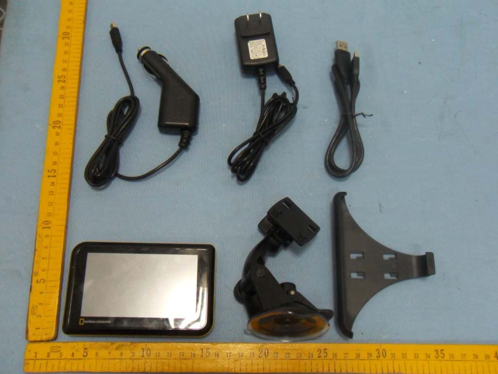
XAJGP430
Jun 27, 2010GPS
Equipment Class
JBP - Part 15 Class B Computing Device Peripheral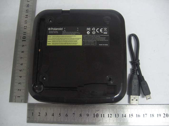
XAJDVD-RW
Jun 24, 2010DVD-RW
Equipment Class
JBP - Part 15 Class B Computing Device Peripheral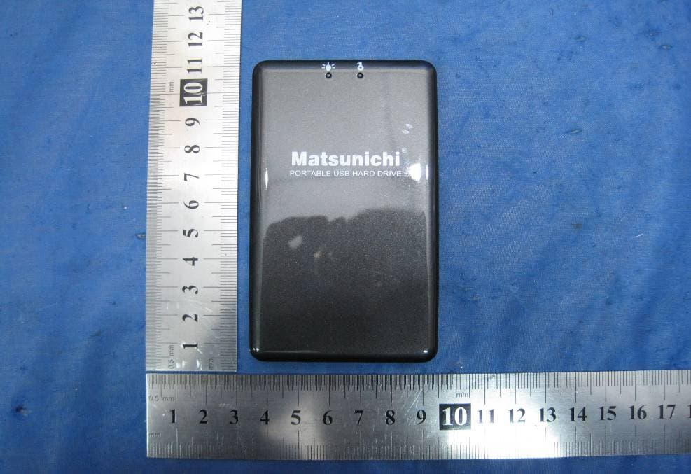
XAJ-DM186
Dec 07, 2009MATSUNICHI MOBILE HARD DISK ENCRYPTION
Equipment Class
JBP - Part 15 Class B Computing Device Peripheral