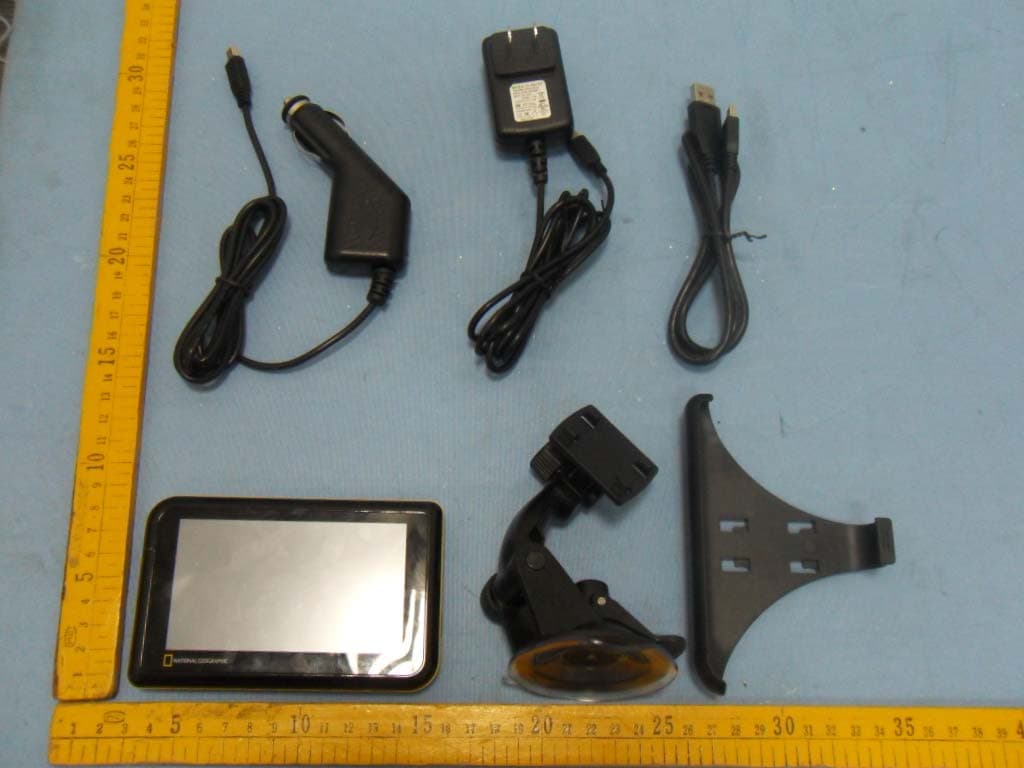
Click to zoom
Application Details
- Equipment Class
- JBP - Part 15 Class B Computing Device Peripheral
- Date of Grant
- Jun 27, 2010
- Application Purpose
- Original Equipment
- Date of Application
- Jun 27, 2010
- Equipment Note
- GPS
- Country
- China
Documents & Files
Document Text
Text extracted from the exhibit documents filed with the FCC. Open a document above to read the original.
Users Manual
www.matsunichi.com.cn 1 2 3 5 6 7 8 10 9 4 感谢您购买本公司的产品,在使用本产品前,请认真阅读本说明书。 1.基本按键介绍 2.功能说明 3.充电器的使用 ① 开机键 ② 拍照键 ③ Mini-SD插口 ④ Mini-USB接口 ⑤ 指示灯 ⑥ 声音控制键 ⑦ 3.5mm耳机接口 ⑧ 摄像头 ⑨ 电池盖 ⑩ GPS支架 2.1 开机/关机 开机:在关机状态下,按住电源开关3~5秒即可开机,开机时会显示松日LOGO。如下图: 2.2 系统主界面 开机后,在系统主界面下,点击屏幕下方的小图标即可切换到该功能的页面,点击右下角的箭 头图标可以翻页查看,翻页时屏幕中间会有动画效果。 2.3 二级界面-系统设置 在此界面下,点击屏幕上的图标即可进入对应的功能,点击右下角的箭头图标可以翻页查看,翻 页时会有动画效果。 3.1 USB充电器 先将充电器插入220V的交流电插座,再将另外一头插入本机USB插口 3.2 汽车充电器 先将汽车充电器的一头插入点烟器插孔内,再将另外一头插入本机的USB插口(如下图)。 休眠/关机:在开机状态下,按住电源键3~5秒,屏幕会出现休眠/关机确认画面,如下图: 在此界面下,点击 按键可进入休眠状态,点击 按键可关机,点击 按键退出此 界面返回到正常操作状态。 休眠唤醒:在休眠状态下,按一下机身上的电源键可退出休眠界面返回到正常操作状态。 序号故 障原因分析解决办法 1 2 3 无法开机 死 机 无法充电 1.电池电量耗尽(按电源键时, 屏幕没有显示)。 请使用充电器为本机充电。 2.在启动界面出现后,长时间停止不动。 取出电池,然后再次装入电池后正常 开机使用 取出电池,然后再次装入电池后正常 开机使用 屏幕不显示,或者有显示但显示不变 且按任何键无效。 在充电时,本机的绿色指示灯没有亮 或屏幕没有显示充电符号。 1.充电器是否插入正确或通电。 2.充电器损坏。 3.电池损坏或电池已充满电。 4.简单故障排除 1 2 3 5 6 7 8 10 9 4 1. Key Introduction 2. Function Introduction ① Power On/Off ② Camera Key ③ Mini-SD Jack ④ Mini-USB Jack ⑤ Indicator ⑥ Volume Control Button ⑦ 3.5mm Earphone Jack ⑧ Camera ⑨ Battery Cap ⑩ GPS Stand 2.1 Power On/Off Power On: In power off status, press the power button for 3~5 seconds to turn on the device, then the "NATIONAL GEOGRAPHIC" LOGO will be displayed on screen. Sleeping&Power Off: In power-on mode, press the power button on the device for 3~5 seconds then the sleeping mode or confirmation for power-off screen will display as follows: THE MANUFACTURER IS NOT RESPONSIBLE FOR ANY RADIO OR TV INTERFERENCE CAUSED BY UNAUTHORIZED MODIFICATIONS TO THIS EQUIPMENT. SUCH MODIFICATIONS COULD VOID THE USER’S AUTHORITY TO OPERATE THE EQUIPMENT. This device complies with Part 15 of the FCC Rules. Operation is subject to the following two conditions: 1. This device may not cause harmful interference, and 2. This device must accept any interference received, including interference that may cause undesired operation. Waking-up from the sleeping: When in sleeping mode, a short press on the power-on button of the device will wake up the system.When in sleeping mode, all the procedure in operation will pause but will back to normal status after waking up. In this UI click the button will be in sleeping mode, click the button will power off; click the button to exit the UI and back to normal operation. Thanks for purchasing our product. Please read this manual carefully before starting to use this device. 20 The c levice wil l be power off in s 2.2 System UI After power on, under this UI, click icon on the left screen to enter the function page. 3. Charger Application 4. Trouble Shooter 2.3 Secondary UI(Customized) Under this UI, click the button on screen to enter the function page. 3.1 USB Charger Take out the USB charger, plug it into the wall outlet with AC 220V (100V~240V), then plug USB line into the USB jack. 3.2 Car Lighter Charger Please insert the car charger into car cigarette lighter jack, then plug into the USB jack(see the illustration below). No.FaultPossible CauseSolutions 1 2 3 No power on Dead Unit Battery drained (The screen has no further display after a blink when pressing power on button.) Please refer to the description of battery charging in this manual, only use the enclosed charger to charge the device. No display of the screen, or display on screen is frozen as any button is pressed. Take out the battery, then put it back, start the device again. Impossible to recharge During charging, the green LED indicator of the device has no light or no charging sign displayed on the screen. If the charger is connected properly and powered. Charger is damaged. Battery is damaged or full charged. 软体: 审核: GP430 简易中文说明书 Simple User Manual FCC NOTE: NOTE: This equipment has been tested and found to comply with the limits for a Class B digital device, pursuant to Part 15 of the FCC Rules. These limits are designed to provide reasonable protection against harmful interference in a residential installation. This equipment generates, uses and can radiate radio frequency energy and, if not installed and used in accordance with the instructions, may cause harmful interference to radio communications. However, there is no guarantee that interference will not occur in a particular installation. If this equipment does cause harmful interference to radio or television reception, which can be determined by turning the equipment off and on, the user is encouraged to try to correct the interference by one or more of the following measures: —Reorient or relocate the receiving antenna. —Increase the separation between the equipment and receiver. —Connect the equipment into an outlet on a circuit different from that to which the receiver is connected. —Consult the dealer or an experienced radio/TV technician for help.
Block Diagram
GP430 Hardware Block Diagram GPS CODEC crystal frequency is 16.367667 MHz. System crystal frequency is 12MHz. System clock crystal frequency is 32.768KHz.
External Photos
FCC ID: XAJGP430 Page 35 o f 39 Anbotek Compliance Laboratory Limited Report No. 201006725F Figure 1 The EUT-Overall View Figure 2 The EUT-Front View FCC ID: XAJGP430 Page 36 o f 39 Anbotek Compliance Laboratory Limited Report No. 201006725F Figure 3 The EUT-Back View
ID Label/Location Info
FCC ID Label Sample for FCC ID:GP430
ID Label/Location Info
The proposed Label Location on EUT Proposed FCC ID Label Location Proposed Label Location on EUT The EUT-Back View/Proposed FCC ID Label Location
Internal Photos
FCC ID: XAJGP430 Page 37 o f 39 Anbotek Compliance Laboratory Limited Report No. 201006725F Figure 4 The EUT-Inside View Figure 5 The EUT-Inside View FCC ID: XAJGP430 Page 38 o f 39 Anbotek Compliance Laboratory Limited Report No. 201006725F Figure 6 The EUT-Inside View Figure 7 PCB of the EUT-Front View FCC ID: XAJGP430 Page 39 o f 39 Anbotek Compliance Laboratory Limited Report No. 201006725F Figure 8 PCB of the EUT-Back View
Operational Description
GP430 Circuit Description This block diagram is SiRF GPS solutions. SiRFatlas IV is a high performance DSP processor, which responsible coordination work for external device. Signal flow: GPS antenna receive satellite signals, amplified and filtered into the decoder, decode the signal out into the main control processing, processing is complete, the final get latitude and longitude and height data. By the data, the maps software can display real time map for users through the LCD. Memory is128M DDR, its function is the data operation. Storage is 4G flash, its function is storage program and user data. Audio processor function is audio decoding and speaker driver. Power chip management charge and discharge for the battery.
Schematics
55 44 33 22 11 D D C C B B A A 55 44 33 22 11 D D C C B B A A SILKSCREEN: 12Mhz OSC 2008.11.12 2008.12.11 GC830 01 CPU-A KEVIN GC830-SCH-B 20 2 ( ) B XINW XINXOUT XOUTW X_SCL_0X_SDA_0 MENU X_SDA_0 9,16 X_SCL_0 9,16 X_SDA_0 9,16 X_SCL_0 9,16 GPS_SPI_CLK 18GPS_SPI_DOUT 18GPS_SPI_CS 18 LCD_ENVEE 14 POWER_ON 10 X_GPIO14 GND GND VDD33 VDD33 VDD_IO GND R210KR0402 R52MR0402 R231KR0402 R8 499R R0402 R7 1M R0402 C3 15pF C0402 R4 4.7K R0402 Y1 32.768KHzXT-2X6 12 3 C4 15pF C0402 R3 4.7K R0402 C215pFC0402 SW2CAMSS305 12 34 Y212MCXA-3225 3 4 R6200KR0402 C115pFC0402 55 44 33 22 11 D D C C B B A A L L L GC830 01 CPU-B KEVIN GC830-SCH-B 20 3 ( ) B X_LDD13 15 X_SD1_DAT3 17 X_LDD15 15 X_LDD2 15 X_LDD0 15 X_L_FCK 15 X_SD1_DAT1 17 X_SD1_PWR_ON 17 X_LDD8 15 X_USB_VBUS 10 X_L_LCK 15 X_USB_DN 10 X_LDD10 15 X_LDD7 15 X_LDD9 15 X_LDD6 15 X_SD1_CLK 17 X_L_PCLK 15 X_L_DE 15 X_SD1_CD_B 17 X_LDD1 15 X_USB_ID 10 X_LDD3 15 X_LDD11 15 X_SD1_DAT2 17 X_LDD4 15 X_LDD12 15 X_USB_DP 10 X_SD1_DAT0 17 X_LDD5 15 X_LDD14 15 C_HSYNC 16 C_VSYNC 16 ID0 16 ID5 16 ID1 16 ID4 16 ID7 16 ID6 16 C_PCLK 16 ID2 16 ID3 16 X_SD1_CMD 17 X_SD1_WP_B 17AV-CNT 16 STAT2_FUL 10 TMC_CD 10 GNDA_USB 55 44 33 22 11 D D C C B B A A ...... 8bit DQS,DQM 400mil 500mil 60mil DDR GC830 01 CPU-C KEVIN GC830-SCH-B 20 4 ( ) B X_MDQS0 7 X_MCLK_O 7 X_MDQM1 7 X_MCAS 7 X_MDQS2 7 X_MCKE 7 X_MDQM0 7 X_MD[31:0] 7 X_MBA0 7 X_MDQS1 7 X_MDQM3 7 X_MCLKB_O 7X_MRAS 7 X_MDQS3 7 X_MA[12:0] 7 X_MCS0 7 X_MDQM2 7 X_MBA1 7 X_MWE 7 55 44 33 22 11 D D C C B B A A H 2008.12.17 CPU 2008.12.30 2009.01.04 GC830 01 CPU-D KEVIN GC830-SCH-B 20 5 ( ) B I2S_MCLK I2S_BCLK 9 I2S_MCLK 9 I2S_DOUT 9 X_FCE_B0 8 I2S_DIN 9 X_DF_RY_BY 8 X_XN 15 X_AUX0 10 I2S_LRCLK 9 X_YP 15 X_YN 15 X_XP 15 LCD_ENVDD 15 X_FCE_B1 8 PCM_CLK 13 PCM_IN 13 PCM_OUT 13 PCM_SYNC 13 CTS_RXD3 13 RTS_TXD3 13 BT_RST 13 BT-CNT 13 TMC_ON R14 33R R0402 C715pFC0402 C10 100pFC0402 12 C11 100pFC0402 12 55 44 33 22 11 D D C C B B A A 3.3V DC/DC 2.5V GC830 01 CPU-E KEVIN GC830-SCH-B 20 6 ( ) B VCC_3V3 VDD_TSCREF25 VDD_IO_LCD VCC_2V5 55 44 33 22 11 D D C C B B A A Serial Resistor 2.5V 2008.10.21 2008.10.22 2008.10.21 GC830 01 Normal DDR KEVIN GC830-SCH-B 20 7 ( ) B MA8 X_MA8 MDQM0 X_MDQM0 MA5 X_MA5 X_MDQM3 MD11 X_MD11 MD30 X_MD30X_MD8 MD8 X_MD3 MD3 MD13 X_MD13X_MD18 MD18 X_MWE MW E X_MD21 MD21 MDQS1 X_MDQS1 X_MA2 MA2 MD19 X_MD19 MD7 X_MD7 X_MCAS MCAS MDQS0 X_MDQS0 X_MDQS2 X_MD17 MD17 X_MRAS MA10 X_MA10 X_MD29 MD29 MA1 X_MA1 X_MD26 MD26 X_MDQM1 MA12 X_MA12 MD22 X_MD22 X_MCAS X_MA7 MA7 MD1 X_MD1 X_MCKE X_MDQM3 MDQM3 X_MDQS3 MDQS3 MD4 X_MD4 MD14 X_MD14 MA11 X_MA11 X_MDQM2 MDQM2 X_MD6 MD6 X_MCS0 MCS0 MA4 X_MA4 X_MCLK_O X_MD31 MD31 X_MD28 MD28 X_MD25 MD25 X_MD20 MD20 X_MBA0 MD5 X_MD5 X_MDQS3 MA9 X_MA9 X_MD0 MD0 X_MA6 MA6 X_MDQS1 X_MCS0 X_MDQM0 X_MBA1 MBA1 MD9 X_MD9 MD16 X_MD16 MD24 X_MD24 X_MCLK_OX_MCLKB_O X_MD2 MD2 X_MBA1 X_MWE X_MCLKB_O MBA0 X_MBA0 X_MDQM2 MDQS2 X_MDQS2 MRAS X_MRAS MD12 X_MD12 MD27 X_MD27 MDQM1 X_MDQM1X_MD10 MD10 MD15 X_MD15 X_MDQS0 MA0 X_MA0 MD23 X_MD23 MA3 X_MA3 X_MD29 X_MA6X_MA2 X_MD9X_MD5X_MD8X_MD28 X_MA7 X_MD7X_MD12X_MD18X_MD16X_MD6X_MD3X_MD26X_MD2X_MD25 MCLK_O X_MD14 X_MA5 MCLKB_O X_MD19 X_MA8 X_MD27X_MD10X_MD23 X_MA9 X_MD21X_MD0 MCKE X_MD11X_MD20 X_MA11 X_MD24X_MD13X_MD1X_MD17 X_MA4X_MA12 X_MD30 X_MA0X_MA1X_MA3 X_MD15 X_MA10 X_MD4X_MD31X_MD22 MBA0 MA6 MCAS MA11MA5 MDQS3 MCS0MCS0 MA2 MBA1MCKEMRAS MDQM1 MCKE MA9MA3MA7MA2MA1MA4 MDQM0 MA1 MRAS MA8 MBA0 MA6 MDQS1 MBA1 MA5MA12MA9 MWEMCLKB_O MA4MA0 MDQS0 MA3 MCAS MA8 MDQM3 MDQS2 MA0 MDQM2 MWEMCLKB_OMCLK_O MA10 MCLK_O MA7MA11MA10MA12 MD10 MD0 MD26 MD7 MD9 MD27 MD20 MD6MD1MD5 MD31 MD18 MD8 MD16 MD25 MD19 MD30 MD23MD21 MD13MD15 MD29 MD4 MD14 MD24 MD2 MD17 MD11 MD28 MD22 MD12 MD3 X_MDQS2 4 X_MCS0 4 X_MWE 4 X_MBA1 4 X_MCLK_O 4 X_MDQM1 4 X_MA[12:0] 4 X_MDQS1 4 X_MD[31:0] 4 X_MCLKB_O 4 X_MCKE 4 X_MDQM0 4 X_MCAS 4 X_MDQM3 4 X_MDQM2 4 X_MDQS0 4 X_MCLK_O 4 X_MRAS 4 X_MCKE 4 X_MBA0 4 X_MDQS3 4 X_MCLKB_O 4 MBA1 4 MA5 4 MBA0 4 MCAS 4 MA0 4 MA4 4 MCAS 4 MA4 4 MCKEMA2 4 MA7 4 MA1 4 MA8 4 MA0 4 MA10 4 MA3 4 MCS0 4 MRAS 4 MA7 4 MCS0 4 MCLK_O MBA1 4 MBA0 4 MA8 4 MA10 4 MA11 4 MA12 4 MA3 4 MWE 4 MRAS 4 MA6 4 MA2 4 MWE 4 MA12 4 MCKEMA9 4 MA6 4 MA1 4 MA11 4 MCLKB_OMCLKB_O MA9 4 MCLK_O MA5 4 VDD2V5 VDD2V5 VDD2V5 VCC_MEM VDD2V5 VREF_DDR VREF_DDR VDD2V5VDD2V5 R21 10R R0402 C33 10nFC0402 12 C42 0.1uFC0402 12 U3 MT46V16M16TOP-66PIN 12345678910111213 14 15 1617 18 1920212223242526274129303132 3334 35363738394028424344454647 4849 5051 52 53 54555657585960616263646566 VDD0 DQ0 VDDQ0 DQ1DQ2 VSSQ0 DQ3DQ4 VDDQ1 DQ5DQ6 VSSQ1 DQ7 NC0 VDDQ2 LDQSA13/NC1 VDD1 NC1LDMWE CASRASCSNC2BA0BA1A11A0A1A2A3 VDD2 VSS0 A4A5A6A7A8A9A10/APA12NC3CKECKCKUDM VSS1 VREF DNU1UDQS VSSQ2 NC4 DQ8 VDDQ3 DQ9 DQ10 VSSQ3 DQ11DQ12 VDDQ4 DQ13DQ14 VSSQ4 DQ15 VSS2 C39 0.1uFC0402 12 R25 10R R0402 C31 10nFC0402 12 R2610KR0402R22120RR0402 U4 MT46V16M16TOP-66PIN 12345678910111213 14 15 1617 18 1920212223242526274129303132 3334 35363738394028424344454647 4849 5051 52 53 54555657585960616263646566 VDD0 DQ0 VDDQ0 DQ1DQ2 VSSQ0 DQ3DQ4 VDDQ1 DQ5DQ6 VSSQ1 DQ7 NC0 VDDQ2 LDQSA13/NC1 VDD1 NC1LDMWE CASRASCSNC2BA0BA1A11A0A1A2A3 VDD2 VSS0 A4A5A6A7A8A9A10/APA12NC3CKECKCKUDM VSS1 VREF DNU1UDQS VSSQ2 NC4 DQ8 VDDQ3 DQ9 DQ10 VSSQ3 DQ11DQ12 VDDQ4 DQ13DQ14 VSSQ4 DQ15 VSS2 C40 10nFC0402 12 C41 0.1uFC0402 12 C28 10nFC0402 12 C30 0.1uFC0402 12 C38 0.1uFC0402 12 R24 10R R0402 C37 0.1uFC0402 12 C29 0.1uFC0402 12 C35 10nFC0402 12 C32 0.1uFC0402 12 C43 0.1uFC0402 12 C36 10nFC0402 12 55 44 33 22 11 D D C C B B A A Boot Configure MLC Nand Flash boot Open drain Pull up to X_PWR_EN K9G8G08....2K/pageK9GAG08....4K/page 2008.10.07 2008.11.12 6b110010 X_TEST_MODE[5:0] INAND Boot 6b001100 Default 6b0010016b1100006b000101 EFuse 11.30 MLC Nand Boot 4KB Page 8 Bit SLC Nand Boot 2KB Page 8 Bit 6b001000 Boot configurationBoundary Scan MLC Nand Boot 2KB Page 8 Bit GC830 01 MLC FLASH KEVIN GC830-SCH-B 20 8 ( ) B X_DF_AD6 X_DF_CLEX_DF_WP_B X_DF_AD4 X_DF_ALE X_DF_AD1 X_FCE_B0 X_DF_CLE X_DF_RY_BY X_DF_RY_BY X_DF_AD0X_DF_AD2 X_DF_AD7 X_FCE_B0 X_DF_AD6 X_DF_RE_B X_DF_AD3 X_DF_WE_B X_DF_WP_B…
Text truncated - open the document above for the full version.
Test Report
FCC ID: XAJGP430 Page 1 o f 39 Anbotek Compliance Laboratory Limited Report No. 201006725F APPLICATION FOR VERIFICATION On Behalf of Matsunichi Communication Holdings R&D (Shenzhen) Co., Ltd. GPS Model No.: GP430 Prepared for : Matsunichi Communication Holdings R&D (Shenzhen) Co., Ltd. Address : 43B/F, INTERNAL CHAMBER OF COMMERCE TOWER, FUHUA RD3 CBD, FUTIAN DISTRICT, SHENZHEN, CHINA Tel: (86) 755-88315408 Fax: (86) 755-88313194 Prepared By : Anbotek Compliance Laboratory Limited Address : 2F, Langfeng Building, Kefa Road North, Hi-tech Industrial Park, Nanshan District, Shenzhen 518057, China Tel: (86) 755-26014771 Fax: (86) 755-26014772 Report Number : 201006725F Date of Test : Jun. 13~23, 2010 Date of Report : Jun. 24, 2010 FCC ID: XAJGP430 Page 2 o f 39 Anbotek Compliance Laboratory Limited Report No. 201006725F TABLE OF CONTENTS Description Page Test Report Verification 1. GENERAL INFORMATION ............................................................................................................... 4 1.1. Description of Device (EUT) ..........................................................................................................................4 1.2. Description of Test Facility.............................................................................................................................5 1.3. Measurement Uncertainty ...............................................................................................................................5 2. POWER LINE CONDUCTED MEASUREMENT ............................................................................ 6 2.1. Test Equipment ...............................................................................................................................................6 2.2. Block Diagram of Test Setup ..........................................................................................................................6 2.3. Power Line Conducted Emission Measurement Limits (FCC Part 15 Class B) .............................................6 2.4. Configuration of EUT on Measurement..........................................................................................................7 2.5. Operating Condition of EUT...........................................................................................................................7 2.6. Test Procedure.................................................................................................................................................7 2.7. Power Line Conducted Emission Measurement Results.................................................................................7 3. RADIATED EMISSION MEASUREMENT..................................................................................... 12 3.1. Test Equipment .............................................................................................................................................12 3.2. Block Diagram of Test Setup ........................................................................................................................12 3.3. Radiated Emission Limit (Subpart B Class B) ..............................................................................................13 3.4. EUT Configuration on Measurement ............................................................................................................13 3.5. Operating Condition of EUT.........................................................................................................................13 3.6. Test Procedure...............................................................................................................................................14 3.7. Radiated Emission Measurement Results .....................................................................................................14 4. PHOTOGRAPH ................................................................................................................................... 31 4.1. Photo of Power Line Conducted Emission Test............................................................................................31 4.2. Photo of Radiated Emission Test ..................................................................................................................32 APPENDIX I (Photos of EUT) (4 Pages) FCC ID: XAJGP430 Page 3 o f 39 Anbotek Compliance Laboratory Limited Report No. 201006725F TEST REPORT VERIFICATION Applicant : Matsunichi Communication Holdings R&D (Shenzhen) Co., Ltd. Manufacturer : Guangzhou Singulargold Electronics Co., Ltd. EUT : GPS Model No. : GP430 Rating : DC 5V via AC/DC Adapter; DC 5V via DC/DC Adapter; DC 3.7V via Battery Trade Mark : NATIONAL GEOGRAPHIC Measurement Procedure Used: FCC Rules and Regulations Part 15 Subpart B 2007 & FCC / ANSI C63.4-2009 The device described above is tested by Anbotek Compliance Laboratory Limited To determine the maximum emission levels emanating from the device. The maximum emission levels are compared to the FCC Part 15 Subpart B Class B limits both radiated and conducted emissions. The measurement results are contained in this test report and Anbotek Compliance Laboratory Limited Is assumed full responsibility for the accuracy and completeness of these measurements. Also, this report shows that the Equipment Under Test (EUT) is to be technically compliant with the FCC requirements. This report applies to above tested sample only. This report shall not be reproduced in part without written approval of Anbotek Compliance Laboratory Limited Date of Test : Jun. 13~23, 2010 Prepared by : (Engineer) Reviewer : (Project Manager) Approved & Authorized Signer : (Manager) FCC ID: XAJGP430 Page 4 o f 39 Anbotek Compliance Laboratory Limited Report No. 201006725F 1. GENERAL INFORMATION 1.1. Description of Device (EUT) Description : GPS Model Number : GP430 Test Power Supply : AC 120V, 60Hz; DC 12V Battery AC/DC Adapter : DYS AC-DC ADAPTER MODEL: DYS06-050150W-1 INP…
Text truncated - open the document above for the full version.
Test Setup Photos
FCC ID: XAJGP430 Page 31 o f 39 Anbotek Compliance Laboratory Limited Report No. 201006725F 4. PHOTOGRAPH 4.1. Photo of Power Line Conducted Emission Test For Charge via AC/DC Adapter Mode For Data Copy Mode FCC ID: XAJGP430 Page 32 o f 39 Anbotek Compliance Laboratory Limited Report No. 201006725F 4.2. Photo of Radiated Emission Test For Data Copy Mode For Charge via DC/DC Adapter Mode FCC ID: XAJGP430 Page 33 o f 39 Anbotek Compliance Laboratory Limited Report No. 201006725F For GPS/Camera Mode For Video/FM Mode
Contact Information
Applicant
Haihua Hu(QC Engineer)
Test Firm
Anbotek Compliance Laboratory limitedDaniel Zhu
Technical Specifications
| # | Rule Parts | Frequency Range | Power Output |
|---|---|---|---|
| 1 | 15B | - | - |
Other Applications from Matsunichi Communication Holdings R&D (Shenzhen) Co., Ltd.
XAJDM253
Jul 28, 2010MOBILE HARD DRIVE
Equipment Class
JBP - Part 15 Class B Computing Device Peripheral
XAJDM189
Jul 28, 2010MOBILE HARD DRIVE
Equipment Class
JBP - Part 15 Class B Computing Device Peripheral
XAJDVD-RW
Jun 24, 2010DVD-RW
Equipment Class
JBP - Part 15 Class B Computing Device Peripheral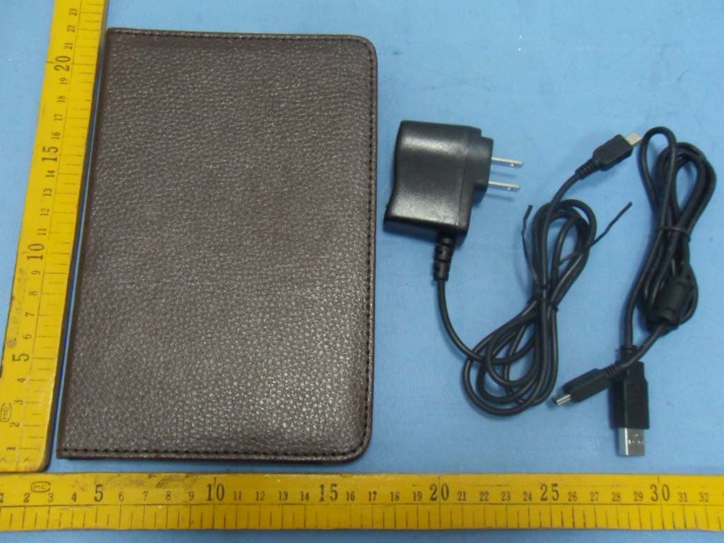
XAJEB602
Jun 23, 2010E-BOOK
Equipment Class
JBP - Part 15 Class B Computing Device Peripheral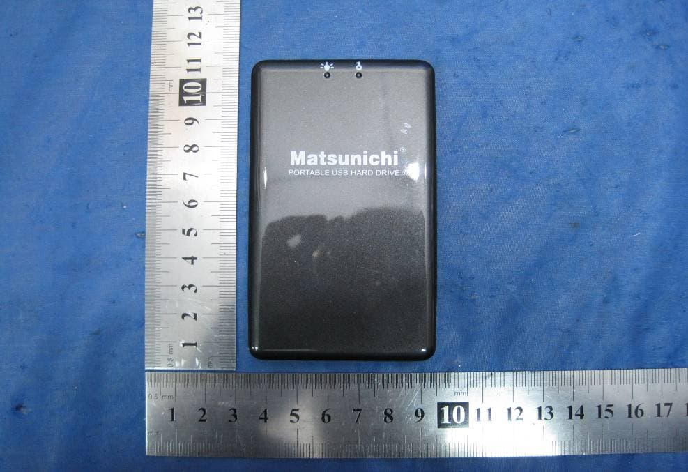
XAJ-DM186
Dec 07, 2009MATSUNICHI MOBILE HARD DISK ENCRYPTION
Equipment Class
JBP - Part 15 Class B Computing Device Peripheral