XDP-GT09011L Digital / 2.4G RF TFT Monitor Receiver
Global Tech China Ltd.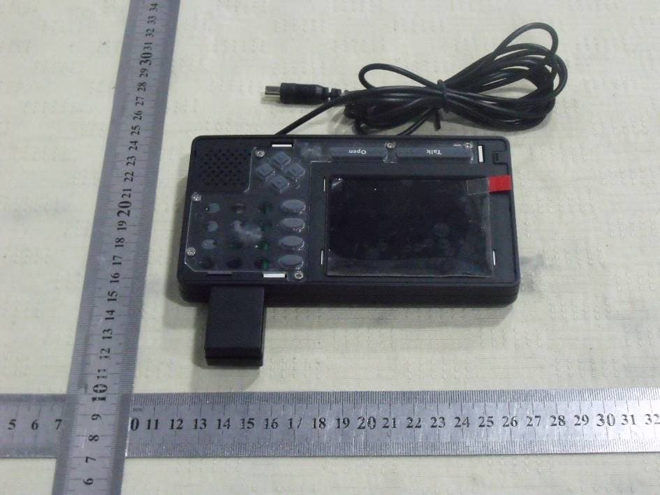
Click to zoom
Application Details
- Equipment Class
- DSS - Part 15 Spread Spectrum Transmitter
- Date of Grant
- Apr 11, 2011
- Application Purpose
- Original Equipment
- Date of Application
- Apr 11, 2011
- Equipment Note
- L Digital / 2.4G RF TFT Monitor Receiver
- Frequency Range
- 2402.00000000 - 2480.00000000
- Company
- Global Tech China Ltd.
- Country
- Hong Kong
Documents & Files
Document Text
Text extracted from the exhibit documents filed with the FCC. Open a document above to read the original.
Users Manual
L Digital Door Entry System Instructions manual Product Features 2.4G Digital Wireless Image Communication 2 Way Wireless Sound Communication Volume Adjustable on Monitor Wireless Door Lock Release Control on Monitor Unit (accessory) Wireless Door Bell Push Button on Door Entry Camera Unit Wireless Digital Zoom Function on Door Entry Camera Unit Wireless Door Camera Motorized Panning Function on Monitor Unit LEDs on Door Entry Camera to Allow Night Viewing Battery Operated Door Camera (optional 6V power adaptor as accessory) Completed Kit contents 1 x 2.4G Wireless TFT Monitor Unit with 1GB SD card 1 x 2.4G Wireless Door Camera Unit 2 x Fixing kits and 1 x instruction manual Optional Accessories Wired or Wireless Door Lock Release Kit Tools required: Small cross head screw driver T-10 Star screw driver Number 6 masonry drill bit A large masonry drill bit (for the Door Entry Camera) Hammer drill Small hammer Pencil, ruler and spirit level Important: before you install the L Digital Door Entry System please take these things into consideration. Position the TFT Screen close to a 13 Amp socket, for the plug-in adapter Keep the TFT out of reach of small children. Choose a position for the TFT, so you can have a clear run with all the power cable. How to install the TFT Using a spirit level and rule, mark and drill 2 holes 7 cm apart using a No. 6 drill bit, then using the wall plugs and screws provided, insert the masonry plugs. Screw the fixing screws into the plugs leaving 2 mm protruding. Attach the TFT on the wall. How to install the Door Entry Camera: When fitting the Door Camera please take into account the position of the sun throughout the year, as the camera view may be affected by direct bright sunlight. Also, if powered by an adaptor, plan the route the power cable will take from the Camera to the mains socket. Using a T-10 star screw driver unscrew the wall mount bracket from the Door Entry Camera. Using the back as a template, mark and drill the 2 mounting holes on the wall. The bottom of the Camera housing should be between 1.2 and 1.4 meters from the ground. If powering the Door Camera by batteries, remove the battery door cover on the rear housing and insert 4 x AA size Batteries. Please replace the battery door on rear housing and mount the Door entry camera unit to the bracket. Using a T-10 star screw driver screw the Door Entry Camera to the wall mount bracket. In normal use, the batteries will last approximately 6 to 9 months. If powering the Door Camera by the 6V adaptor, insert the jack plug to the socket on the Door Camera. Using a T-10 star screw driver screw the Door Entry Camera to the wall mount bracket. IMPORTANT: The Door Camera has a built-in power save mode whereby, if powered by Batteries only, it will shut down into sleep mode one minute after the “Call Button” is pressed . This sleep mode will not be activated if the Camera is powered by the 6V adaptor, which means that the Door Camera will be in View Mode at all times after power-up. Note that Alkaline batteries will power the Door Camera for approx 50 days (based on 5 activations a day) whereas Lithium batteries will last for approx 90 days. How to install the wired or wireless door release (optional accessory) Please use the diagram below as a guide Please consult the I/M that comes with these items. System Operation The system is very easy to operate. When a visitor presses the CALL button on the wireless Door Camera, the electronic door bell will sound at the TFT monitor unit. Please press any buttons on the monitor and the camera view will appear on that monitor’s TFT screen (If you have a multi-camera system installed, you may need to press the CAM SELECT button on the Monitor to bring up the Door Camera view). Note that if the Door Camera is being powered by batteries only, then, after 60 seconds, the image will disappear and the Door Camera will automatically revert to its power saving sleep mode. Press the CALL button again at the Door Camera to re-establish an image on the TFT screen. If the visitor is not within the camera view, move the camera Right or Left by using the camera’s Panning control buttons. You can talk to the visitor by pressing the Monitor’s TALK button. To listen to the visitor speak, release the TALK button (make sure the volume level is correct). There is no need for the visitor to press the CALL button again to speak to you (unless the Door Camera has reverted to its power saving sleep mode, in which case the visitor should press the CALL button again). The Door Camera has built-in night view LEDs so you can see your visitor at night, although, because CCTV cameras have limited picture visibility in the dark, even with infra-red LEDs, there is a limited range of view at night. Therefore, if the image is still dark, you may want to add a separate PIR activated light above the camera to give additional background light If you have a Door Lock Release added to the system, you can let your visitor in by pressing the OPEN button on the monitor unit. Note: The TFT Monitor will also revert to its power saving mode 2 minutes after any button was last pressed. Push Button Functionality On the TFT Monitor Unit On the Door Camera Individual Buttons on the TFT Monitor On the Side of the Monitor, there is a small switch that selects Monitor Off, Power Down On or Off. If Power Down has been selected, it means the unit will power down 2 minutes after a button has last been pressed. If Power Down has not been selected, it means that the Monitor will remain constantly in View Mode, including audio from the camera in view. 1. Mode Button SD Card Inserted : In View mode, press the Mode button once to change to Playback mode or press the MODE button and hold for 3 seconds to change to Setup mode. In either case, press once again to change back to View mode No SD Card Inserted : In View mode, press the Mode button once to change to Setup mode, press once again to change back to View mode 2. Camera…
Text truncated - open the document above for the full version.
Block Diagram
Block diagram
Cover Letter(s)
SCS-F18: Project and Product Certification Representative Authorization Letter Page 1 of 2 Rev 2.0 2206 Ringwood Avenue San Jose, CA 95131 Tel: 408-526-1188 Fax: 408-526-1088 Email: [email protected] Project and Product Certification Representative Authorization Letter Revision History Reason for Amendment (current / obsolete) From To Approved Date Initial Release (current) 1.0 1.0 Nov-14-2006 Revised wording (current) 1.0 2.0 Sept–25-2007 SCS-F18: Project and Product Certification Representative Authorization Letter Page 2 of 2 Rev 2.0 GLOBAL TECH CHINA LTD. 2011-3-24 To: SIEMIC, INC. 2206 Ringwood Avenue, San Jose, CA 95131 USA Dear Sir/Madam, Re: Project and Product Certification Representative Authorization Letter We, GLOBAL TECH CHINA LTD. hereby authorize SIEMIC, INC. to act as a Certification Body for certifying for the following project(s): (L DIGITAL / 2.4G RF TFT MONITOR RECEIVER, GT09011) We affirm that between SIEMIC and GLOBAL TECH CHINA LTD. any difference in understanding, including test plan, measurement methods, applicable standards and relevant procedures and processes have been resolved prior to commencement of testing activities. Sincerely, Signature Kendy lee E-mail: : [email protected] Phone: +852-28844318 Fax: +852-28844816 Address : Room 12, 14th Floor, Tower 2, Evergain Plaza, 88 Container Port Road, Kwai Chung, HongKong
External Photos
External of EUT
ID Label/Location Info
FCC ID Label FCC ID: XDP-GT09011 Model Number: GT09011 Made in China This device complies with Part 15 of the FCC Rules. Operation is subject to the following two conditions: (1) this device may not cause harmful interference, and (2) this device must accept any interference received, including interference that may cause undesired operation
ID Label/Location Info
Label Location Proposed Label Location on EUT
Internal Photos
Internal of EUT Internal of EUT Internal of EUT Wireless module Internal of EUT
Operational Description
L Digital Operation Description Product feature 2.4G Wireless Digital camera Image with Audio communication Pan motor control from 2.4G Wireless Receiver Direct AV out from 2.4G wireless Receiver Two way sound communication Operation Camera image data through TX module transfer RF datae and the Receiver module Asic progressing Audio and Video direct output from TFT display, Pan Key control from RX module Asic function processor detail Audio In/Out Processor Video In/Out Processor KeyPad control Buit In CPU 2.4G wireless module
RF Exposure Info
RF EXPOSURE EVALUATION According to FCC 1.1310: The criteria listed in the following table shall be used to evaluate the environment impact of human exposure to radio frequency(RF) Radiation as specified in §1.1307(b) Limits for Maximum Permissible Exposure(MPE) Frequency Range(MHz) Electric Field Strength(V/m) Magnetic Field Strength(A/m) Power Density(mW/cm 2 ) Average Time (A) Limits for Occupational/Control Exposures 300-1500 -- -- F/300 6 1500-100000 -- -- 5 6 (B) Limits for General Population/Uncontrol Exposures 300-1500 -- -- F/1500 6 1500-100000 -- -- 1 30 1.1 Friis transmission formula: Pd=(Pout*G)\(4*pi*R 2 ) Where Pd= Power density in mW/cm 2 Pout=output power to antenna in mW G= gain of antenna in linear scale Pi=3.1416 R= distance between observation point and center of the radiator in cm Pd the limit of MPE, 1mW/cm 2 . If we know the maximum gain of the antenna and total power input to the antenna, through the calculation, we will know the distance where the MPE limit is reached. 1.2 Measurement Result . Antenna gain: 1 dBi Channel Channel Frequency (MHz) Output Peak power (dBm) Output Peak power (mW) Antenna Gain (dBi) Power density at 20cm (mW/ cm 2 ) Power density Limits (mW/cm 2 ) 1 2402.00 12.88 19.41 1 0.004826 1 6 2440.00 13.05 20.18 1 0.005018 1 11 2480.00 12.91 19.54 1 0.004859 1
Schematics
1 2 3 4 5 6 7 8 9 10 11 12 ABCD 12 11 10 9 8 7 6 5 4 3 2 1 D CBA VCC_2V5 X12M_IN VCC_2V5 SYS_3V3 VCC_2V5 Pairing_MODE V_D5 X12M_OUT SYS_3V3 DGND VCC_2V5 SYS_3V3 DGND V_D4 SW6 SYS_3V3 SYS_3V3 DGND DGND V_D3 V_D7 S_SDA VCC_2V5 SW3 SYS_3V3 V_D0 S_SCL VCC_2V5 V_D6 SYS_3V3 V_D9 VCC_2V5 DGND SW5 VCC_2V5 DGND V_D15 SW4 V_D14 DGND DGND VCC_2V5 V_D2 DGND VCC_2V5 VCC_2V5 DGND V_D8 VCC_2V5 SYS_3V3 DGND DGND V_D1 SYS_3V3 SYS_3V3 V_D10 V_D11 V_D12 V_D13 DGND USB_DN USB_DP SYS_3V3 VCC_2V5 DGNDUSB_DET VCC_2V5 C4222uF C560.1uF C590.1uF R33 100R C620.1uFC610.1uF C440.1uF C640.1uFC630.1uF C450.1uF 1 2 R12 1K C700.1uF R32 100R C650.1uF C460.1uF C490.1uF C580.1uF C670.1uF C480.1uF C510.1uF C600.1uF C690.1uF C500.1uF C530.1uF C660.1uF 12 C3210uF C520.1uF C550.1uF C4722uF 1 2 R13 1K C680.1uF C540.1uF 12 C3110uF C570.1uF S_SDAS_SCL SYS_3V3 DGND SYS_3V3 DGND VCC_2V5 VCC_2V5 VCC_3V DGND ROMD1 I2S_LRC ROMD4 L01_MISO I2S_BCLK ROMA3 ROMA12ROMA10 ROMA4 ROMA11 L01_CS L01_ENROMA7 NROMRD NROMCE ROMD0ROMA0ROMA1ROMA8 L01_NSSROMA13 L01_MOSI ROMD6ROMA2ROMA5ROMA9 L01_SCLK ROMD7 NROMWR I2S_MCLK ROMA6 I2S_ADC ROMD2ROMD3 I2S_DAC ROMD5 ROMA14 RST V_BS1V_UDQMV_A10V_A7SWDMASS_INV_CASV_A2V_A8V_CSV_LDQMV_CKENEAV_A9V_A6V_A5 TEST0 V_BS0V_WEV_A12V_A0V_A1V_RASV_A11V_A3V_CLKV_A4 V_D[0..15] V_D[0..15] ROMA15ROMA16 SPI_DATASPI_CLKSPI_ACS L01_IRQ_OUT RXD0TXD0 X12M_INX12M_OUT C36 22pF 34 12 X112MHz C37 22pF DGND DGND USB_DN USB_DET USB_DP R34 270R C43 0.1uF R36 100K R4320K R41 3K R42 10K R35 270R DGND VUSB USB interface VUSB R2410K R14NC R15NC R16NCR2510K R2310K R260R NEA TEST0 SWD MASS_IN DGND DGND SYS_3V3 DGND SYS_3V3 DGND SYS_3V3 R313k C110.1uF RST DGND SYS_3V3 S_MCLK1 S_IMG9 S_IMG8 S_IMG4 S_IMG6 S_IMG3 S_IMG2 S_IMG7 S_VSYNC S_IMG5 S_HSYNC R11 0R R110R S_PCLK S_MCLK S_MCLK C1180pF DGND R3 100R C3 47pF R4 100R C4 47pF S_IMG2S_IMG3 R5 100R C5 47pF R6 100R C6 47pF S_IMG4S_IMG5 R7 100R C7 47pF R8 100R C8 47pF S_IMG6S_IMG7 R9 100R C9 47pF R10 100R C10 47pF S_IMG8S_IMG9 R2 100R C2 47pF S_PCLK DGND N01N02N03N04N05N06N07N08N09 RY10R SYS_3V3 VCC_3V S_PCLK USB_DN_INUSB_DP_IN 1234 JA3CON4 VCC_3V DGND AU_DOWN X32K_IN C33 10pF C3410pF DGND DGND X32K_OUT 1 23 4 X232.768KHz X32K_IN X32K_OUT VCC_2V5 SYS_3V3 C8822p L01_MOSIL01_MISOL01_SCLK L01_NSS L01_EN L01_CS RF33V DGND C87 3.3pF 12345678910 SIP110 HEADER L01_IRQ_OUT CF147uF CF21uF DGND DGND RF33V SYS_3V3 RN1100R LOUTROUT MODE SPK_IN SPI_CLKSPI_DATASPI_ACS MODE XAUD_IN R4947k C290.1uF C8610uF R48470k C270.1uF C732200pF C220.1uF MICIN 22 RLINEIN 23 LLINEIN 24 MODE 25 CSB 26 SDIN 27 SCLK 28 XT/MCLK 1 XTO 2 DCVDD 3 DGND 4 DBVDD 5 CLKOUT 6 BLCK 7 DACDAT 8 DACLRC 9 ROUT 17 LOUT 16 HPGND 15 RHPOUT 14 LHPOUT 13 HPVDD 12 ADCLRC 11 ADCDAT 10 AVDD 18 AGND 19 VMID 20 MICBIAS 21 U6WM8731(L) C210.1uF C30 0.1uF R5410k R28 0R C7410uF/16V R29 100R C8510uF I2S_BCLK I2S_DACI2S_ADC I2S_MCLK I2S_LRC SPI_DATASPI_CLKSPI_ACS DGND AU_3V I2S33V I2S_AGND AU_3V DGND IS233V I2S_AGND I2S33V I2S_AGND I2S_AGND I2S_AGND I2S33V C280.1uF I2S_AGND C38100pF I2S_AGND Q5 BC847w R6110k R663.3k R673.3k I2S_AGND I2S_AGND C8310uF I2S_AGND C841uF I2S33V R5510k C781pF R53No R301k Vin 1 GND 2 SHD 3 CC 4 Vout 5 U7 EMP8935-30VF05GRR C79100nF I2S_AGND I2S_AGND 3.0V RA110R AU_3V VCC_3V SPK OUTSPK GND M1 MICROPHONE1 LHPOUT DGND I2S_AGND 1234 5678 U5SPK AP RU2 1k CU1 1uF RU11K I2S_AGND I2S_AGND RU52K CU510uF/16V CU41uF SPK_IN CU20.039uF RU320K SD +5V I2S_AGND RU6100R AU_DOWN R17NC R20NCR19NC C170.1uF R47470k R18NC DQ0 2 CAS 17 DQ1 4 RAS 18 DQ2 5 VSS 28 DQ3 7 CS 19 DQ4 8 WE 16 DQ5 10 VCC 1 DQ6 11 VSSQ 6 DQ7 13 CLK 38 VSSQ 12 VSS 41 VCCQ 3 VSS 54 VSSQ 52 BS0 20 CKE 37 VSSQ 46 VCCQ 9 VCC 14 BS1 21 VCC 27 A0 23 VCCQ 43 A1 24 UDQM 39 A2 25 A3 26 A4 29 A5 30 A6 31 A7 32 A8 33 A9 34 A10/AP 22 A11 35 VCCQ 49 DQ8 42 DQ9 44 DQ10 45 DQ11 47 DQ12 48 DQ13 50 DQ14 51 DQ15 53 LDQM 15 A12 36 NC 40 U4SDRAM 64M/128M/256M C140.1uFC180.1uF C200.1uF C71 22uF/16V C150.1uFC190.1uF C160.1uF V_D0V_D1V_D2V_D3V_D4V_D5V_D6V_D7V_D8V_D9V_D10V_D11V_D12V_D13V_D14V_D15 V_A0V_A1V_A2V_A3V_A4V_A5V_A6V_A7V_A8V_A9 V_A10V_BS0 V_CASV_RAS V_WE V_UDQM V_LDQM V_CKEV_CLK V_CS V_A11V_A12V_BS1 V_BS0 V_BS1 DGND SD_3V SD_3V DGND SD_3V DGND SD_3V SD_3V SD_3V SD_3V SD_3V SD_3V DGND DGND DGND DGND DGND DGND SD_3V DGND SD_3V DGND RS10R SD_3V VCC_3V NROMCE ROMA0 ROMA5 ROMA3ROMD7 ROMA7ROMA13 ROMA2ROMA1ROMD6ROMA10 ROMA14 ROMD4 ROMA6 ROMD0 ROMA8 ROMD1ROMD2NROMRD ROMA4 ROMD5ROMD3 ROMA15ROMA16NROMW RROMA9ROMA11ROMA12 R464.7k C130.1uF R454.7k R444.7k A11 1 A9 2 A8 3 A13 4 A14 5 A17 6 WE 7 VDD 8 A18 9 A16 10 A15 11 A12 12 A7 13 A6 14 A5 15 A4 16 OE 32 A10 31 CE 30 D7 29 D6 28 D5 27 D4 26 D3 25 VSS 24 D2 23 D1 22 D0 21 A0 20 A1 19 A2 18 A3 17 U3 SST_FLASH_TSOP R27100R ROMD0ROMD1ROMD2ROMD3ROMD4ROMD5ROMD6ROMD7 ROMA4ROMA5ROMA6ROMA7ROMA8 ROMA10 ROMA11ROMA12ROMA13ROMA14ROMA15ROMA16 NROMRD NROMCE NROMWR ROMA9 ROMA0ROMA1ROMA2ROMA3 SF_3V SF_3V SF_3V DGND DGND DGND ROMA17 ROMA17 ROMA18 ROMA18 RF1100R SF_3V SYS3V3 MR8980A MARS 23456789 101112131415161718192021222324252627282930313233343536373839404142434445464748495051525354 55 56 57 58 59 60 61 62 63 64 65 66 67 68 69 70 71 72 73 74 75 76 77 78 79 80 87 88 89 90 91 92 93 94 95 96 97 98 100 101 102 103 104 105 106 107 108 109110111 165 164 163 162161160159158157156155154153152151150149148147146145144143142141140139138137136135134133132131130129128127126125124123122121120119118117114113112 216 215 214 213 212 211 210 209 208 207 206 205 204 203 202 201 200 199 198 197 196 195 194 193 192 191 190 189 188 187 186 185 184 183 182 181 180 179 178 177 176 175 174 173 172 171 170 169 168 167 166 1 81 82 83 84 85 86 99 115116 U1LQFP-216 1 2 3 4 5 6 7 8 9 10 11 12 ABCD 12 11 10 9 8 7 6 5 4 3 2 1 D CBA VCC_2V5 X12M_IN VCC_2V5 SYS_3V3 VCC_2V5 SW1_MODE V_D5 X12M_OUT SYS_3V3 DGND VCC_2V5 SYS_3V3 DGND MIC_DOW N V_D4 SW6 SYS_3V3 SYS_3V3 DGND DGND V_D3 V_D7 VCC_2V5 SW3 SYS_3V3 V_D0 VCC_2V5 V_CKEV_D6 SYS_3V3 V_D9 VCC_2V5 DGND SW5 VCC_2V5 X27M_IN DGND V_CLKV_D15 SW4 V_D14 DGND DGND VCC_2V5 V_LDQM V_D2 POWER DGND X27M_OUT VCC_2V5 VCC_2V5 DGND V_D8 VCC_2V5 SYS_3V3DGND DGND V_D1 SYS_3V3 SYS_3…
Text truncated - open the document above for the full version.
Test Report
SHENZHEN EMTEK CO., LTD. REPORT NO: ES101009017F FCC ID: XDP-GT09011 DATE: 3/24/2011 Page 1 of 41 ELECTROMAGNETIC EMISSIONS COMPLIANCE REPORT INTENTIONAL RADIATOR CERTIFICATION TO FCC PART 15 SUBPART C REQUIREMENT OF L Digital / 2.4G RF TFT Monitor Receiver MODEL No.: GT09011 FCC ID: XDP-GT09011 REPORT NO: ES101009017F ISSUE DATE: March 24, 2011 Prepared for GLOBAL TECH CHINA LTD. Room 12, 14th Floor, Tower 2, Evergain Plaza, 88 Container Port Road, Kwai Chung, HongKong Prepared by SHENZHEN EMTEK CO., LTD Bldg 69, Majialong Industry Zone, Nan0shan District, Shenzhen, Guangdong, China TEL: 86-755-26954280 FAX: 86-755-26954282 SHENZHEN EMTEK CO., LTD. REPORT NO: ES101009017F FCC ID: XDP-GT09011 DATE: 3/24/2011 Page 2 of 41 VERIFICATION OF COMPLIANCE Applicant: GLOBAL TECH CHINA LTD. Room 12, 14th Floor, Tower 2, Evergain Plaza, 88 Container Port Road, Kwai Chung, HongKong Manufacturer: GLOBAL TECH CHINA LTD. Room 12, 14th Floor, Tower 2, Evergain Plaza, 88 Container Port Road, Kwai Chung, HongKong Product Description: L Digital / 2.4G RF TFT Monitor Receiver Brand Name: N/A Model Number: GT09011 Serial Number: N/A File Number: ES101009017F Date of Test: January 31, 2011 to March 17, 2011 We hereby certify that: The above equipment was tested by SHENZHEN EMTEK CO., LTD. The test data, data evaluation, test procedures, and equipment configurations shown in this report were made in accordance with the procedures given in ANSI C63.4 (2009) and the energy emitted by the sample EUT tested as described in this report is in compliance with conducted and radiated emission limits of FCC Rules Part 15.247. The test results of this report relate only to the tested sample identified in this report. Approved By David Lee / Q.A. Manager SHENZHEN EMTEK CO., LTD. SHENZHEN EMTEK CO., LTD. REPORT NO: ES101009017F FCC ID: XDP-GT09011 DATE: 3/24/2011 Page 3 of 41 Ta b l e o f C o n t e n t s 1. GENERAL INFORMATION ................................................................................................. 5 1.1 P RODUCT DESCRIPTION.............................................................................................................. 5 1.2 RELATED SUBMITTAL(S) / GRANT (S).......................................................................................... 6 1.3 T EST METHODOLOGY................................................................................................................. 6 1.4 S PECIAL ACCESSORIES................................................................................................................ 6 1.5 E QUIPMENT MODIFICATIONS...................................................................................................... 6 1.6 T EST FACILITY............................................................................................................................ 6 2. SYSTEM TEST CONFIGURATION .................................................................................... 7 2.1 EUT CONFIGURATION................................................................................................................ 7 2.2 EUT EXERCISE........................................................................................................................... 7 2.3 T EST PROCEDURE....................................................................................................................... 7 2.4 L IMITATION................................................................................................................................7 2.5 C ONFIGURATION OF TESTED SYSTEM....................................................................................... 11 3. DESCRIPTION OF TEST MODES .................................................................................... 12 4. CONDUCTED EMISSIONS TEST ..................................................................................... 13 4.1 M EASUREMENT PROCEDURE:.................................................................................................... 13 4.2 T EST SET-UP (BLOCK DIAGRAM OF CONFIGURATION)............................................................ 13 4.3 M EASUREMENT EQUIPMENT USED: .......................................................................................... 13 4.4 CONDUCTED EMISSION LIMIT................................................................................................... 13 4.5 M EASUREMENT RESULT: .......................................................................................................... 14 4.6 CONDUCTED MEASUREMENT PHOTOS:...................................................................................... 15 5. RADIATED EMISSION TEST ............................................................................................ 16 5.1 M EASUREMENT PROCEDURE..................................................................................................... 16 5.2 T EST SET-UP (BLOCK DIAGRAM OF CONFIGURATION)............................................................ 16 5.3 M EASUREMENT EQUIPMENT USED: .......................................................................................... 17 5.4 RADIATED EMISSION LIMIT........................................................................................................ 17 5.5 MEASUREMENT RESULT............................................................................................................ 18 5.6 RADIATED MEASUREMENT PHOTOS: ......................................................................................... 24 6. CHANNEL SEPARATION TEST ....................................................................................... 25 6.1 M EASUREMENT PROCEDURE..................................................................................................... 25 6.2 T EST SET-UP (BLOCK DIAGRAM OF CONFIGURATION)............................................................ 25 6.3 M EASUREMENT EQUIPMENT USED: ........................................................................…
Text truncated - open the document above for the full version.
Test Setup Photos
RADIATED EMISSION TEST CONDUCTED EMISSION TEST
Contact Information
Applicant
Kendy lee
Test Firm
EMTEK (Shenzhen) Co., Ltd.David Lee
Technical Specifications
| # | Rule Parts | Frequency Range | Power Output |
|---|---|---|---|
| 1 | 15C | 2.40 GHz - 2.48 GHz | 20.00 mW |
Other Applications from Global Tech China Ltd.
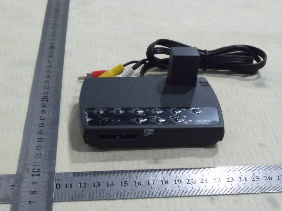
XDP-GT09013
Apr 11, 2011I Digital / 2.4G RF DVR Receiver
Equipment Class
DSS - Part 15 Spread Spectrum Transmitter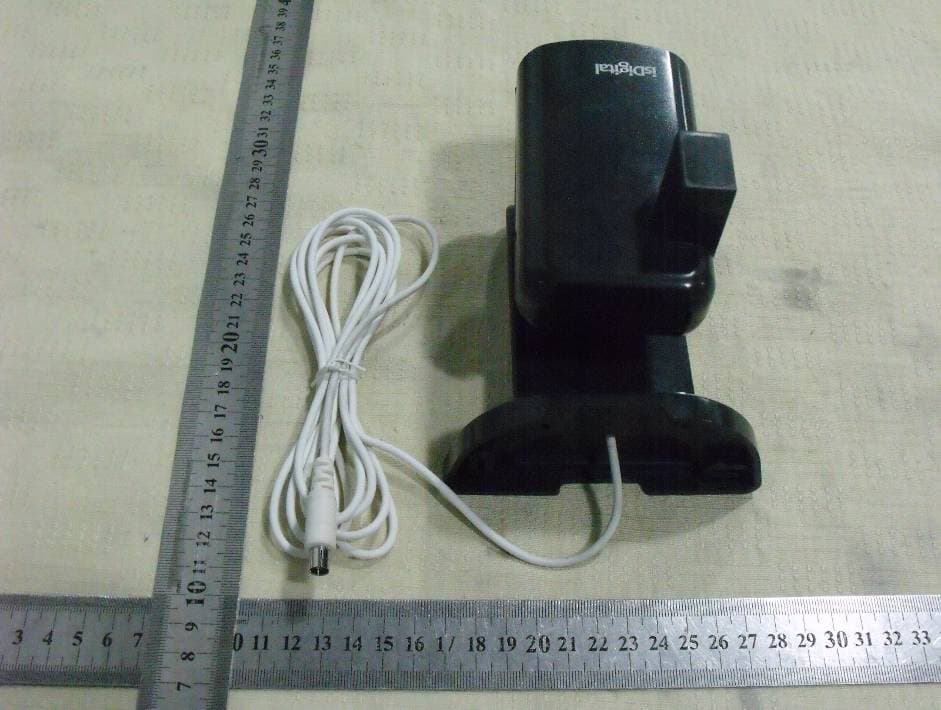
XDP-GT09012
Mar 14, 2011I Digital / 2.4G RF PanTilt Camera (Transmitter)
Equipment Class
DSS - Part 15 Spread Spectrum Transmitter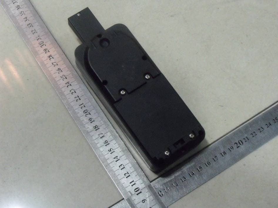
XDP-GT09010
Feb 24, 2011L Digital / 2.4G RF Door Entry Camera (Transmitter)
Equipment Class
DSS - Part 15 Spread Spectrum Transmitter