XKB-IUP250-WDPayment Terminal
INGENICO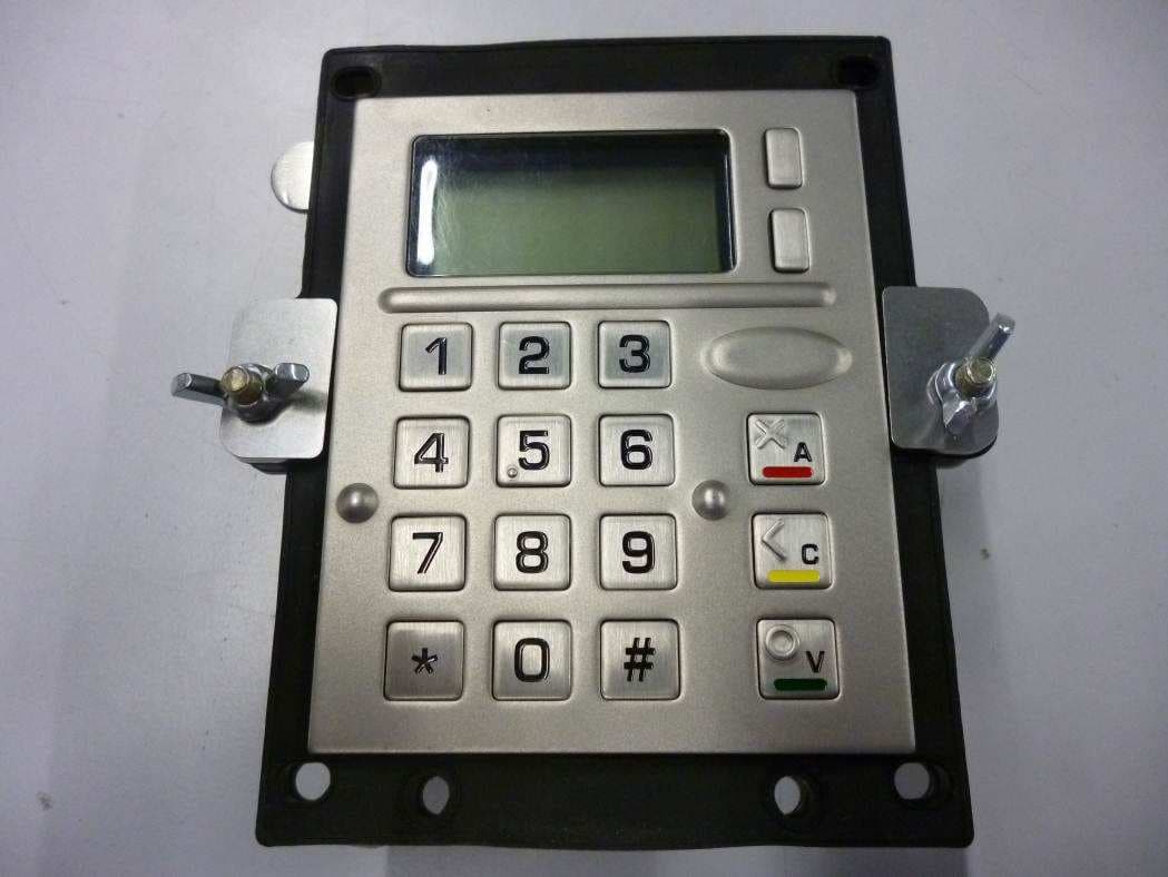
Click to zoom
Application Details
- Equipment Class
- JBP - Part 15 Class B Computing Device Peripheral
- Date of Grant
- Aug 29, 2012
- Application Purpose
- Original Equipment
- Date of Application
- Aug 29, 2012
- Equipment Note
- Payment Terminal
- Company
- INGENICO
- Country
- France
Documents & Files
Document Text
Text extracted from the exhibit documents filed with the FCC. Open a document above to read the original.
Users Manual
Ingenico – 28-32 Boulevard de Grenelle - 75015 PARIS Tél. 33(0)1 58 01 80 00 - Fax 33 (0)1 58 01 91 35 iUP 250 & iUR 250 I n t é g r a t i o n G u i d e Intégration Guide_iUP250&iUR250 2/83 Copyright © 2012 Ingenico 900009151 R11 000 01/1223 All rights reserved The scope of this document is to assist third party integrators when dealing with Ingenico UNattended products (iUN) such as iUP250 and iUR250, both certified PCI PTS 3.x, or others. It offers all information needed for a successful integration of iUP250 and iUR250 products into unattended kiosk machines. For any sales information please refer to your Ingenico contact into the region. Updates table Version Date Nature of modifications Author Visa 1.0 17/11/2011 First version D.GEORGES 2.0 01/06/2012 Official version D.GEORGES Intégration Guide_iUP250&iUR250 3/83 Copyright © 2012 Ingenico 900009151 R11 000 01/1223 All rights reserved Table of contents 1 GENERAL ............................................................................................................. 6 1.1 Definition of acronyms ..................................................................................... 6 1.2 iUP250 & iUR250 payment solution presentation .......................................... 7 1.2.1 Diagram of iUP250 & iUR250 connectivity and communications .................. 8 1.2.2 Examples of integration ................................................................................ 9 1.2.3 Services ...................................................................................................... 10 1.3 Description of modules .................................................................................. 11 1.3.1 iUP250 ........................................................................................................ 11 1.3.1.1 Technical Hardware characteristics ...................................................... 12 1.3.1.2 iUP250 output connectors description .................................................. 14 1.3.1.3 SAM & μSD Installation ........................................................................ 22 1.3.1.4 Buzzer ................................................................................................... 22 1.3.1.5 RGB backlight ....................................................................................... 23 1.3.1.6 Maintenance Button .............................................................................. 23 1.3.1.7 Cable Protection ................................................................................... 24 1.3.1.8 Antenna Installation .............................................................................. 25 1.3.1.9 PINPad and Reader interconnectivity ................................................... 26 1.3.2 iUR250 ........................................................................................................ 27 1.3.2.1 Technical Hardware Characteristics ..................................................... 28 1.3.2.2 iUR250 output connectors description .................................................. 29 1.3.2.3 RGB Leds ............................................................................................. 31 1.3.2.4 iUR250 Optional Lever Lock ................................................................. 31 1.4 Professional installation Requirement ......................................................... 32 2 MAIN ACCESSORIES ........................................................................................ 33 2.1.1 Generality ................................................................................................... 33 2.1.2 Optional PINPad-to-Reader USB cable ...................................................... 33 2.1.3 iUP250 Power supply ................................................................................. 33 2.1.4 Stand-by management cable ...................................................................... 33 2.1.5 Optional Pinshield ....................................................................................... 34 3 SOFTWARE ........................................................................................................ 37 3.1 iUP250 .............................................................................................................. 37 3.1.1 Software Architecture ................................................................................. 38 3.1.2 Secure management of software ................................................................ 39 3.1.3 Operating system ........................................................................................ 40 3.1.4 TELIUM MANAGER ................................................................................... 41 3.1.5 Software downloading ................................................................................ 43 3.1.6 Development station ................................................................................... 45 3.2 iUR250 ............................................................................................................. 47 Intégration Guide_iUP250&iUR250 4/83 Copyright © 2012 Ingenico 900009151 R11 000 01/1223 All rights reserved 3.2.1 Software architecture .................................................................................. 48 3.2.2 Software security management .................................................................. 48 3.2.3 Operating system ........................................................................................ 49 4 TERMINAL MANAGEMENT SYSTEM ............................................................... 50 4.1 Introduction ..................................................................................................... 50 4.2 Basic functions ............................................................................................... 50 4.3 Advanced functions ....................................................................................…
Text truncated - open the document above for the full version.
Attestation Statements
1/1 Attestation The application designed by the FCC ID: XKB-IUP250-WD is only a Class B computing device peripheral without any intentional radiators except for a GPRS option with modular approval (FCC ID: VW3HILOV2). If the GPRS module is used in this application, I attest that we follow all the installation instructions and grant conditions of the GPRS module. Marc Delorme Quality Manager 9 Avenue de la Gare Rovaltain TGV BP 25156 26958 Valence Cedex 9
Cover Letter(s)
July 20 th , 2012 CONFIDENTIALITY REQUEST Curtis-Straus LLC One Distribution Center Circle #1 Littleton, MA 01460 USA Re: Confidentiality request for a Digital Device FCC ID: XKB-IUP250-WD Gentlemen, INGENICO SA requests, pursuant to 47CFR 0.459, post grant confidentiality for portions of the material contained in this application. The following document regarding this submission for FCC ID: XKB-IUP250-WD shall be kept confidential: 1. Block Diagram (File: Block Diagram - XKB-IUP250-WD.pdf) Specifically, these exhibits contain information relating to circuit function and complexity that could be of benefit to competitors. The material contains trade secrets and confidential information that INGENICO does not customarily release to the public and which is otherwise not generally available to the public. Regards, Marc DELORME Quality Manager
External Photos
FCC ID: XKB-IUP250-WD Page 1/4 EXTERNAL PHOTOS OF TESTED EUT FCC ID: XKB-IUP250-WD Page 2/4 FCC ID: XKB-IUP250-WD Page 3/4 FCC ID: XKB-IUP250-WD Page 4/4 Difference with GPRS module
ID Label/Location Info
FCC ID: XKB-IUP250-WD Page 1/5 PRODUCT LABELING FCC ID / IC number label Place of label FCC ID: XKB-IUP250-WD Page 2/5 FCC ID: XKB-IUP250-WD Page 3/5 Configuration n°1 FCC ID: XKB-IUP250-WD Page 4/5 Configuration n°2 FCC ID: XKB-IUP250-WD Page 5/5 Configuration n°3
Internal Photos
FCC ID: XKB-IUP250-WD Page 1/10 INTERNAL PHOTOS OF TESTED EUT FCC ID: XKB-IUP250-WD Page 2/10 FCC ID: XKB-IUP250-WD Page 3/10 FCC ID: XKB-IUP250-WD Page 4/10 FCC ID: XKB-IUP250-WD Page 5/10 FCC ID: XKB-IUP250-WD Page 6/10 FCC ID: XKB-IUP250-WD Page 7/10 FCC ID: XKB-IUP250-WD Page 8/10 OPTION PCB – COM2 + MDB: FCC ID: XKB-IUP250-WD Page 9/10 OPTION PCB – COM2 + MDB+GPRS MODULAR APPROVAL: FCC ID: XKB-IUP250-WD Page 10/10 Modular Approval GPRS
Operational Description
FCC ID: XKB-IUP250-WD Page 1/5 OPERATIONAL DESCRIPTION 1.1. EUT description FCC ID: XKB-IUP250-WD Page 2/5 FCC ID: XKB-IUP250-WD Page 3/5 1.2. Related Submittal(s) / Grant(s) All host equipment used in the test configuration are FCC granted, when relevant. 1.3. Tested System Details The FCC IDs for all equipment, plus description of all cables used in the tested system are: The system was configured for testing in a typical fashion (as a customer would normally use it). The equipment IUP250 can be used with several internal option cards: COM2 + MDB Configuration n°2 COM2 + MDB + GPRS modular approval Configuration n°3 The Equipment Under Test will be the configuration n°3 to represent others configurations (Worst case) IUP250 has to be is integrated in unattended devices. The test configuration is given by the manufacturer Internal max frequencies: 400MHz Modular Approval contained: - 1 x GPRS module, SAGEMCOM , HILO V2 INGENICO, FCC ID: VW3HILOV2 Power supply: 12-30Vdc EUT is not sold with any power supply, an AC/DC power supply adapter is used to provide 12VDC (worst case) during whole tests.(worst case) Input/output: - 1 x MDB slave port “DC power input (12-30VDC)“ - 2 x Serial link (COM0 & COM 2) - 1 x Ethernet line - 1 x USB port (Slave) - 4 x USB ports (Host) - 1 x MDB Master (4 wires). “ - 1 x 5V output port - 2 x SAMs slot - 1 x SIM slot - 1 x MicroSD slot - 1 x SMA connector, (GSM) Cables/Accessories: - 1 x AC power cord, 2 wires, unshielded: 2m - 1 x DC power supply cable (fixed on mains power unit), unshielded: 1.75m - 1 x Ethernet cable Type: STP Cat 5e, shielded: 2m - 5 x USB cables, shielded, (4 x spiraled: 1m & 1x non spiraled: 1m) - 2 x RS232 Com cables, RJ11, unshielded, 1.5 m (COM 0 & Com 2) - 1 x MdB-slave ‘6 pins’ <-> MdB- master ‘8 pins’ cable, unshielded - 1 x Jack cable , unshielded, length: 0.3cm - 1 x GPRS Antenna type, length: 200cm FCC ID: XKB-IUP250-WD Page 4/5 Auxiliaries equipment used during test: - 1 x Laptop TOSHIBA SATELLITE PS141E-04YC sn : 13594938G - 1 x AC/DC Power supply adapter PHIHONG PSM36W-120TW, 100-240VAC / 1.5A / 50-60Hz, output 12VDC / 3A Functions: - 1 x SAM card reader - 1 x Serial link communication (COM0 & COM2) - 1 x μSD card reader (SAM1 & SAM2) A generic program test is loaded on EUT, in order to perform in loop following functions: - Reading / writing SAM card (SAM1 & SAM2) - Reading / writing μSD card (MMC) - Continous loop communication From RX/TX on Serial port (COM0 & COM2) - Continous Ethernet communication is performed from EUT to Laptop (Ping) FCC ID: XKB-IUP250-WD Page 5/5 1.4. Test Methodology Both conducted and radiated testing were performed according to the procedures in ANSI C63.4-2003, FCC Part 15 Subpart B. Radiated testing was performed at an antenna to EUT distance of 10 meters. During testing, all equipment’s and cables were moved relative to each other in order to identify the worst case set-up. 1.5. Test facility Tests have been performed from February 2 nd to 28 th , 2012. This test facility has been fully described in a report and accepted by FCC as compliant with the radiated and AC line conducted test site criteria in ANSI C63.4-2003 in a letter dated March 25 th , 2008 (registration number 94821). This test facility has also been accredited by COFRAC (French accreditation authority for European Union test lab accreditation organization) according to NF EN ISO/IEC 17025, accreditation number 1-1633 as compliant with test site criteria and competence in 47 CFR Part 15/ANSI C63.4 and EN55022/CISPR22 norms for 89/336/EEC European EMC Directive application. All pertinent data for this test facility remains unchanged.
Test Report
Rapport d’essai / Test report N° 249987-R2-E JDE : 110606 DELIVRE A / ISSUED TO : INGENICO 9 Avenue de la Gare Rovaltain TGV - BP 25156 26958 VALENCE Cedex 9 Objet / Subject : Essais de compatibilité électromagnétique conformément aux normes FCC CFR 47 Part 15, Subpart B Electromagnetic compatibility tests according to the standards FCC CFR 47 Part 15, Subpart B Matériel testé / Apparatus under test : Produit / Product : Clavier pour automate banquaire / Bank automate keyboard Marque / Trade mark : INGENICO Constructeur / Manufacturer : INGENICO Type / Model : IUP250 N° de série / serial number : PROTO FCC ID : XKB-IUP250-WD Date des essais / Test date : Du 8 au 28 Février 2012 / From February 8 th to 28 th , 2012 Lieu d’essai / Test location : LCIE SUD-EST ZI Centr’Alp – 170 rue de Chatagnon 38430 MOIRANS - FRANCE Test réalisé par / Test performed by : Jonathan PAUC Ce document comporte /Composition of document : 17 pages. MOIRANS, LE 19 JUILLET 2012, JULY 19TH, 2012 Ecrit par / Written by, Approuvé par / Approved by, Anthony MERLIN Jacques LORQUIN La reproduction de ce document n'est autorisée que sous sa forme intégrale. Toute reproduction partielle ou toute insertion de résultats dans un texte d'accompagnement en vue de leur diffusion doit recevoir un accord préalable et formel du LCIE. Ce document résulte d’essais effectués sur un spécimen, un échantillon ou une éprouvette. Il ne préjuge pas de la conformité de l’ensemble des produits fabriqués à l’objet essayé. Sauf indication contraire, la décision de conformité prend en compte l’incertitude de mesures. Il ne préjuge en aucun cas d’une décision de certification. This document shall not be reproduced, except in full, without the written approval of the LCIE. This document contains results related only to the item tested. It does not imply the conformity of the whole production to the item tested .Unless otherwise specified; the decision of conformity takes into account the uncertainty of measures. This document does not anticipate any certification decision. RAPPORT D'ESSAI / TEST REPORT N° 249987-R2-E Page : 2 / 17 SUMMARY 1. TEST PROGRAM ............................................................................................................................... 3 2. SYSTEM TEST CONFIGURATION ..................................................................................................... 4 3. CONDUCTED EMISSION DATA......................................................................................................... 6 4. RADIATED EMISSION DATA ............................................................................................................. 8 6. ANNEX 1 (GRAPHS) ........................................................................................................................ 13 7. UNCERTAINTIES CHART ................................................................................................................ 17 RAPPORT D'ESSAI / TEST REPORT N° 249987-R2-E Page : 3 / 17 1. TEST PROGRAM Standard: - FCC Part 15, Subpart B (Digital Devices) - ANSI C63.4 (2003) EMISSION TEST LIMITS RESULTS (Comments) Limits for conducted disturbance at mains ports 150kHz-30MHz Frequency Quasi-peak value (dBμV) Average value (dBμV) COMPLY 150-500kHz 66 to 56 56 to 46 0.5-5MHz 56 46 5-30MHz 60 50 Radiated emissions 30MHz-12.5GHz* Measure at 3m 30MHz-88MHz : 40 dBμV/m 88MHz-216MHz : 43.5 dBμV/m 216MHz-960MHz : 46.0 dBμV/m Above 960MHz : 54.0 dBμV/m COMPLY *§15.33: The highest internal source of a testing device is defined like more the highest frequency generated or used in the testing device or on which the testing device works or agrees. - If the highest frequency of the internal sources of the testing device is lower than 108 MHz, measurement must be only performed until 1GHz. - If the highest frequency of the internal sources of the testing device ranges between 108 MHz and 500 MHz, measurement must be only performed until 2GHz. - If the highest frequency of the internal sources of the testing device ranges between 500 MHz and 1 GHz, measurement must be only performed until 5GHz. If the highest frequency of the internal sources of the testing device is above 1 GHz, measurement must be only performed until 5 times the highest frequency or 40 GHz, while taking smallest of both. RAPPORT D'ESSAI / TEST REPORT N° 249987-R2-E Page : 4 / 17 2. SYSTEM TEST CONFIGURATION 2.1. JUSTIFICATION The system was configured for testing in a typical fashion (as a customer would normally use it). The equipment IUP250 can be used with several internal option cards: COM2 + MDB Configuration n°2 COM2 + MDB + GPRS modular approval Configuration n°3 The Equipment Under Test will be the configuration n°3 to represent others configurations (Worst case) IUP250 has to be is integrated in unattended devices. The test configuration is given by the manufacturer 2.2. HARDWARE IDENTIFICATION Equipment under test (EUT): IUP250 Serial number: PROTO FCC ID: XKB-IUP250-WD Internal max frequencies: 400MHz Modular Approval contained: - 1 x GPRS module, SAGEMCOM , HILO V2 INGENICO, FCC ID: VW3HILOV2 Power supply: 12-30Vdc EUT is not sold with any power supply, an AC/DC power supply adapter is used to provide 12VDC (worst case) during whole tests.(worst case) Input/output: - 1 x MDB slave port “DC power input (12-30VDC)“ - 2 x Serial link (COM0 & COM 2) - 1 x Ethernet line - 1 x USB port (Slave) - 4 x USB ports (Host) - 1 x MDB Master (4 wires). “ - 1 x 5V output port - 2 x SAMs slot - 1 x SIM slot - 1 x MicroSD slot - 1 x SMA connector, (GSM) Cables/Accessories: - 1 x AC power cord, 2 wires, unshielded: 2m - 1 x DC power supply cable (fixed on mains power unit), unshielded: 1.75m - 1 x Ethernet cable Type: STP Cat 5e, shielded: 2m - 5 x USB cables, shielded, (4 x spiraled: 1m & 1x non spiraled: 1m) - 2 x RS232 Com cables, RJ11, unshielded, 1.5 m (COM 0 & Com 2) - 1 x MdB-slave ‘6 pins’ <-> MdB- master ‘8 pins’ cable, unshielded - 1 x Ja…
Text truncated - open the document above for the full version.
Test Setup Photos
FCC ID: XKB-IUP250-WD Page 1/2 1 CONDUCTED AND RADIATED MEASUREMENT PHOTO 1.1 Conducted emission FCC ID: XKB-IUP250-WD Page 2/2 1.2 Radiated emission
Contact Information
Applicant
Nicolas Jacquemont(Certification Manager)
Test Firm
LCIE Sud-EstJacques Lorquin
Technical Specifications
| # | Rule Parts | Frequency Range | Power Output |
|---|---|---|---|
| 1 | 15B | - | - |
Other Applications from INGENICO
XKB-DX8AM
Aug 06, 2026Smart POS Terminal
Equipment Class
PCB - PCS Licensed TransmitterXKB-INGA02WF
Apr 03, 2026Smart Module
Equipment Class
DSS - Part 15 Spread Spectrum TransmitterXKB-INGA02WU
Mar 25, 2026Smart Module
Equipment Class
DTS - Digital Transmission SystemXKB-MOBEM3TOC
Dec 24, 2025Mobile Payment Terminal
Equipment Class
DXX - Part 15 Low Power Communication Device Transmitter
XKB-RX9CLWBT
Aug 26, 2024Payment terminal
Equipment Class
NII - Unlicensed National Information Infrastructure TX