XMR2021RM502QGL5G Sub-6 GHz M.2 Module
Quectel Wireless Solutions Company Limited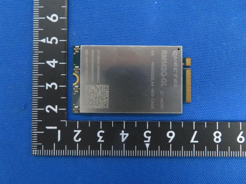
Click to zoom
Application Details
- Equipment Class
- CBE - Citizens Band End User Devices
- Date of Grant
- May 31, 2021
- Application Purpose
- Original Equipment
- Date of Application
- May 31, 2021
- Equipment Note
- 5G Sub-6 GHz M.2 Module
- Frequency Range
- 3552.50000000 - 3697.50000000
- Country
- China
Documents & Files
Document Text
Text extracted from the exhibit documents filed with the FCC. Open a document above to read the original.
Users Manual
RM502Q-GL Hardware Design 5G Module Series Rev. RM502Q-GL_Hardware_Design_V1.0 Date: 2020-07-06 Status: Preliminary www.quectel.com 5G Module Series RM502Q-GL Hardware Design RM502Q-GL_Hardware_Design 1 / 77 Our aim is to provide customers with timely and comprehensive services. For any assistance, please contact our company headquarters: Quectel Wireless Solutions Co., Ltd. Building 5, Shanghai Business Park Phase III (Area B), No.1016 Tianlin Road, Minhang District, Shanghai 200233, China Email: [email protected] Or our local office. For more information, please visit: http://www.quectel.com/support/sales.htm For technical support, or to report documentation errors, please visit: http://www.quectel.com/support/technical.htm Or email to: [email protected] GENERAL NOTES QUECTEL OFFERS THE INFORMATION AS A SERVICE TO ITS CUSTOMERS. THE INFORMATION PROVIDED IS BASED UPON CUSTOMERS’ REQUIREMENTS. QUECTEL MAKES EVERY EFFORT TO ENSURE THE QUALITY OF THE INFORMATION IT MAKES AVAILABLE. QUECTEL DOES NOT MAKE ANY WARRANTY AS TO THE INFORMATION CONTAINED HEREIN, AND DOES NOT ACCEPT ANY LIABILITY FOR ANY INJURY, LOSS OR DAMAGE OF ANY KIND INCURRED BY USE OF OR RELIANCE UPON THE INFORMATION. ALL INFORMATION SUPPLIED HEREIN IS SUBJECT TO CHANGE WITHOUT PRIOR NOTICE. COPYRIGHT THE INFORMATION CONTAINED HERE IS PROPRIETARY TECHNICAL INFORMATION OF QUECTEL WIRELESS SOLUTIONS CO., LTD. TRANSMITTING, REPRODUCTION, DISSEMINATION AND EDITING OF THIS DOCUMENT AS WELL AS UTILIZATION OF THE CONTENT WITHOUT PERMISSION ARE FORBIDDEN. OFFENDERS WILL BE HELD LIABLE FOR PAYMENT OF DAMAGES. ALL RIGHTS ARE RESERVED IN THE EVENT OF A PATENT GRANT OR REGISTRATION OF A UTILITY MODEL OR DESIGN. Copyright © Quectel Wireless Solutions Co., Ltd. 2020. All rights reserved. 5G Module Series RM502Q-GL Hardware Design RM502Q-GL_Hardware_Design 2 / 77 About the Document Revision History Version Date Author Description 1.0 2020-07-06 Kingson ZHANG/ Qiqi WANG Initial 5G Module Series RM502Q-GL Hardware Design RM502Q-GL_Hardware_Design 3 / 77 Contents About the Document ................................................................................................................................... 2 Contents ....................................................................................................................................................... 3 Table Index ................................................................................................................................................... 5 Figure Index ................................................................................................................................................. 6 1 Introduction .......................................................................................................................................... 8 1.1. Safety Information ....................................................................................................................... 9 2 Product Concept ................................................................................................................................ 10 2.1. General Description .................................................................................................................. 10 2.2. Key Features ............................................................................................................................. 11 2.3. Functional Diagram ................................................................................................................... 13 2.4. Evaluation Board ....................................................................................................................... 14 3 Application Interfaces ....................................................................................................................... 15 3.1. Pin Assignment ......................................................................................................................... 16 3.2. Pin Description .......................................................................................................................... 17 3.3. Power Supply ............................................................................................................................ 21 3.3.1. Decrease Voltage Drop .................................................................................................. 21 3.3.2. Reference Design for Power Supply .............................................................................. 22 3.4. Turn on and off Scenarios ......................................................................................................... 23 3.4.1. Turn on the Module ........................................................................................................ 23 3.4.1.1. Turn on the Module with a Host GPIO ................................................................ 24 3.4.1.2. Turn on the Module Automatically ...................................................................... 24 3.4.1.3. Turn on the Module with Compatible Design ...................................................... 25 3.4.2. Turn off the Module ........................................................................................................ 26 3.4.2.1. Turn off the Module through FULL_CARD_POWER_OFF# .............................. 26 3.4.2.2. Turn off the Module through AT Command ........................................................ 26 3.5. Reset ......................................................................................................................................... 28 3.6. (U)SIM Interfaces ...................................................................................................................... 30 3.7. USB Interface ............................................................................................................................ 32 3.8. PCIe Interface ...................................…
Text truncated - open the document above for the full version.
External Photos
Report No.: 2101RSU049-UE 1 of 1 EUT Photograph (1) EUT Photo (2) EUT Photo
ID Label/Location Info
Label Location
Internal Photos
Report No.: 2101RSU049-UE 1 of 1 EUT Photograph (1) EUT Photo (2) EUT Photo
RF Exposure Info
MRT Technology (Suzhou) Co., Ltd Report No.: 2101RSU049-U8 Phone: +886-3-3288388 Report Version: V01 Web: www.mrt-cert.com Issue Date: 05-22-2021 1 of 10 RF Exposure Evaluation Declaration FCC ID: XMR2021RM502QGL Application: Quectel Wireless Solutions Company Limited Application Type: Certification Product: 5G Sub-6 GHz M.2 Module Model No.: RM502Q-GL Brand Name: Quectel Test Procedure(s): KDB 447498 D01v06 Test Date: February 05 ~ May 18, 2021 Reviewed By: Sunny Sun Approved By: Robin Wu The test results relate only to the samples tested. The test results shown in the test report are traceable to the national/international standards through the calibration of the equipment and evaluated measurement uncertainty herein. The test report shall not be reproduced except in full without the written approval of MRT Technology (Suzhou) Co., Ltd. Report No.: 2101RSU049-U8 2 of 10 Revision History Report No. Version Description Issue Date Note 2101RSU049-U8 Rev. 01 Initial Report 05-22-2021 Valid Report No.: 2101RSU049-U8 3 of 10 1. GENERAL INFORMATION 1.1. Applicant Quectel Wireless Solutions Company Limited Building 5, Shanghai Business Park Phase III (Area B), No.1016 Tianlin Road, Minhang District, Shanghai, China 200233 1.2. Manufacturer Quectel Wireless Solutions Company Limited Building 5, Shanghai Business Park Phase III (Area B), No.1016 Tianlin Road, Minhang District, Shanghai, China 200233 1.3. Testing Facility Test Site - MRT Suzhou Laboratory Laboratory Location (Suzhou - Wuzhong) D8 Building, No.2 Tian’edang Rd., Wuzhong Economic Development Zone, Suzhou, China Laboratory Location (Suzhou - SIP) 4b Building, Liando U Valley, No.200 Xingpu Rd., Shengpu Town, Suzhou Industrial Park, China Laboratory Accreditations A2LA: 3628.01 CNAS: L10551 FCC: CN1166 ISED: CN0001 VCCI: R-20025, G-20034, C-20020, T-20020 Test Site - MRT Shenzhen Laboratory Laboratory Location (Shenzhen) 1G, Building A, Junxiangda Building, Zhongshanyuan Road West, Nanshan District, Shenzhen, China Laboratory Accreditations A2LA: 3628.02 CNAS: L10551 FCC: CN1284 ISED: CN0105 Test Site - MRT Taiwan Laboratory Laboratory Location (Taiwan) No. 38, Fuxing 2 nd Rd., Guishan Dist., Taoyuan City 333, Taiwan (R.O.C.) Laboratory Accreditations TAF: L3261-190725 FCC: 291082, TW3261 ISED: TW3261 Report No.: 2101RSU049-U8 4 of 10 1.4. Product Information Product Name 5G Sub-6 GHz M.2 Module Model No. RM502Q-GL Brand Name Quectel Operating Temperature -30 ~ 70 °C Power Type 3.135 ~ 4.4Vdc, typical 3.7Vdc UMTS Specification Single Band Band 2, 4, 5 Modulation Uplink up to 16QAM, Downlink up to 64QAM E-UTRA Specification Single Band Band 2, 4, 5, 7, 12, 13, 14, 17, 25, 26, 30, 38, 41, 48, 66, 71 Intra-Band CA_2C, CA_5B, CA_7C, CA_38C, CA_41C, CA_48C, CA_66C HPUE Band Band 41 Modulation UL & DL up to 256QAM 5G NR Specification SA Band n2, n7, n5, n12, n25, n41, n66, n71, n77 SA UL MIMO Band n41, n77 EN-DC Band DC_25A_n41A, DC_26A_n41A, DC_2A_n41A, DC_66A_n41A DC_4A_n41A, DC_2A_n77A, DC_7A_n77A, DC_12A_n77A, DC_41A_n77A, DC_66A_n77A HPUE Band n41, n77 (SA & UL MIMO) SCS for NR cell FDD Band: 15kHz; TDD Band: 30kHz Modulation UL & DL up to 256QAM Report No.: 2101RSU049-U8 5 of 10 2. RF Exposure Evaluation 2.1. Limits According to FCC 1.1310: The criteria listed in the following table shall be used to evaluate the environment impact of human exposure to radio frequency (RF) radiation as specified in 1.1307(b) Limits for Maximum Permissible Exposure (MPE) Frequency Range (MHz) Electric Field Strength (V/m) Magnetic Field Strength (A/m) Power Density (mW/cm 2 ) Average Time (Minutes) (A) Limits for Occupational/ Control Exposures 300-1500 -- -- f/300 6 1500-100,000 -- -- 5 6 (B) Limits for General Population/ Uncontrolled Exposures 300-1500 -- -- f/1500 6 1500-100,000 -- -- 1 30 f= Frequency in MHz Calculation Formula: Pd = (Pout*G)/(4*pi*r 2 ) Where Pd = power density in mW/cm 2 Pout = output power to antenna in mW G = gain of antenna in linear scale Pi = 3.1416 r = distance between observation point and center of the radiator in cm Pd is the limit of MPE, 1mW/cm². If we know the maximum gain of the antenna and the total power input to the antenna, through the calculation, we will know the distance r where the MPE limit is reached. Report No.: 2101RSU049-U8 6 of 10 2.2. Test Result of RF Exposure Evaluation Product 5G Sub-6 GHz M.2 Module Test Item RF Exposure Evaluation Test Mode Frequency Band (MHz) Maximum Conducted Power (dBm) Antenna Gain (dBi) ERP (EIRP) (dBm) Power Density at 20cm (mW/cm 2 ) Limit (mW/ cm 2 ) WCDMA B2 1850 ~ 1910 25.00 8.00 33.00 0.3969 1.0000 WCDMA B4 1710 ~ 1755 25.00 5.00 30.00 0.1989 1.0000 WCDMA B5 824 ~ 849 25.00 5.00 30.00 0.1989 0.5493 LTE B2 1850 ~ 1910 25.00 8.00 33.00 0.3969 1.0000 LTE B4 1710 ~ 1755 25.00 5.00 30.00 0.1989 1.0000 LTE B5 824 ~ 849 25.00 5.00 30.00 0.1989 0.5493 LTE B7 2500 ~ 2570 25.00 8.00 33.00 0.3969 1.0000 LTE B12 699 ~ 716 25.00 5.00 30.00 0.1989 0.4660 LTE B13 777 ~ 787 25.00 5.00 30.00 0.1989 0.5180 LTE B14 788 ~ 798 25.00 5.00 30.00 0.1989 0.5253 LTE B17 704 ~ 716 25.00 5.00 30.00 0.1989 0.4693 LTE B25 1850 ~ 1915 25.00 8.00 33.00 0.3969 1.0000 LTE B26 814 ~ 849 25.00 5.00 30.00 0.1989 0.5427 LTE B30 2305 ~ 2315 25.00 -1.02 23.98 0.0497 1.0000 LTE B38 2570 ~ 2620 28.00 5.00 33.00 0.3969 1.0000 LTE B41 2496 ~ 2690 28.00 5.00 33.00 0.3969 1.0000 LTE B48 3550 ~ 3700 25.00 -2.00 23.00 0.0397 1.0000 LTE B66 1710 ~ 1780 25.00 5.00 30.00 0.1989 1.0000 LTE B71 663 ~ 698 25.00 5.00 30.00 0.1989 0.4420 Report No.: 2101RSU049-U8 7 of 10 Test Mode Frequency Band (MHz) Maximum Conducted Power (dBm) Antenna Gain (dBi) ERP (EIRP) (dBm) Power Density at 20cm (mW/cm 2 ) Limit (mW/ cm 2 ) n2 1850 ~ 1910 25.00 8.00 33.00 0.3969 1.0000 n5 824 ~ 849 25.00 5.00 30.00 0.1989 0.5493 n7 2500 ~ 2570 25.00 8.00 33.00 0.3969 1.0000 n12 699 ~ 716 25.00 5.00 30.00 0.1989 0.4660 n25 1850 ~ 1915 25.00 8.00 33.00 0.3969 1.0000 n41 2496 ~ 2690 28.00 5.00 33.00 0.3969 1.0000 n66 1710 ~ 1780 25.00 5.00 30.00 0.198…
Text truncated - open the document above for the full version.
Test Report
MRT Technology (Suzhou) Co., Ltd Report No.: 2101RSU049-U1 Phone: +86-512-66308358 Report Version: V02 Web: www.mrt-cert.com Issue Date: 05-31-2021 1 of 78 FCC ID: XMR2021RM502QGL Application: Quectel Wireless Solutions Company Limited Application Type: Certification Product: 5G Sub-6 GHz M.2 Module Model No.: RM502Q-GL Brand Name: Quectel FCC Rule Part(s): Part 96 Test Procedure(s): ANSI C63.26: 2015 Test Date: January 21 ~ May 30, 2021 Reviewed By: Sunny Sun Approved By: Robin Wu MEASUREMENT REPORT FCC PART 96 The test results relate only to the samples tested. This equipment has been shown to be capable of compliance with the applicable technical standards as indicated in the measurement report and was tested in accordance with the measurement procedures specified in ANSI C63.26-2015. Test results reported herein relate only to the item(s) tested. The test report shall not be reproduced except in full without the written approval of MRT Technology (Suzhou) Co., Ltd. Report No.:2101RSU049-U1 2 of 78 Revision History Report No. Version Description Issue Date Note 2101RSU049-U1 Rev. 01 Initial Report 05-19-2021 Invalid 2101RSU049-U1 Rev. 02 Added EIRP of full bandwidth 05-31-2021 Valid Report No.:2101RSU049-U1 3 of 78 CONTENTS Description Page 1. GENERAL INFORMATION ...................................................................................................... 5 1.1. Applicant ...................................................................................................................... 5 1.2. Manufacturer ................................................................................................................ 5 1.3. Testing Facility .............................................................................................................. 5 1.4. Product Information ...................................................................................................... 6 1.5. Radio Specification under Test ..................................................................................... 6 1.6. Description of Available Antennas ................................................................................. 7 1.7. Test Methodology ......................................................................................................... 7 1.8. EMI Suppression Device(s)/Modifications ..................................................................... 7 1.9. Maximum Power, Frequency Tolerance, and Emission Designator .............................. 8 1.10. Configuration of Tested System ................................................................................... 9 1.11. Test Environment Condition .......................................................................................... 9 2. TEST EQUIPMENT CALIBRATION DATE ............................................................................. 10 3. MEASUREMENT UNCERTAINTY ......................................................................................... 12 4. TEST RESULT ....................................................................................................................... 13 4.1. Summary .................................................................................................................... 13 4.2. Occupied Bandwidth Measurement ............................................................................ 14 4.2.1. Test Limit ................................................................................................................ 14 4.2.2. Test Procedure ....................................................................................................... 14 4.2.3. Test Setting ............................................................................................................. 14 4.2.4. Test Setup .............................................................................................................. 14 4.2.4.1. Test Result .............................................................................................................. 15 4.3. Frequency Stability Measurement .............................................................................. 23 4.3.1. Test Limit ................................................................................................................ 23 4.3.2. Test Procedure ....................................................................................................... 23 4.3.3. Test Setting ............................................................................................................. 23 4.3.4. Test Setup .............................................................................................................. 24 4.3.5. Test Result .............................................................................................................. 25 4.4. Equivalent Isotropically Radiated Power Measurement .............................................. 26 4.4.1. Test Limit ................................................................................................................ 26 4.4.2. Test Procedure ....................................................................................................... 26 4.4.3. Test Setting ............................................................................................................. 26 4.4.4. Test Setup .............................................................................................................. 27 4.4.5. Test Result .............................................................................................................. 28 4.5. Band Edge Measurement ........................................................................................... 40 Report No.:2101RSU049-U1 4 of 78 4.5.1. Test Limit ................................................................................................................ 40 4.5.2. Test Procedure ........................................................................................…
Text truncated - open the document above for the full version.
Test Report
Report No.:2101RSU049-U1 47 of 78 20MHz Channel Bandwidth - 1RB Low Channel ACP MiddleChannel ACP - Low RB Position MiddleChannel ACP - High RB Position High Channel ACP Extended Band Edge Report No.:2101RSU049-U1 48 of 78 5MHz Channel Bandwidth - Full RB Low Channel ACP Middle Channel ACP Extended Band Edge (3612.5 ~ 3621.5MHz) Extended Band Edge (3628.5 ~ 3637.5MHz) High Channel ACP Report No.:2101RSU049-U1 49 of 78 10MHz Channel Bandwidth - Full RB Low Channel ACP Middle Channel ACP High Channel ACP Extended Band Edge Report No.:2101RSU049-U1 50 of 78 15MHz Channel Bandwidth - Full RB Low Channel ACP Middle Channel ACP High Channel ACP Extended Band Edge Report No.:2101RSU049-U1 51 of 78 20MHz Channel Bandwidth - Full RB Low Channel ACP Middle Channel ACP High Channel ACP Extended Band Edge Report No.:2101RSU049-U1 52 of 78 Product 5G Sub-6 GHz M.2 Module Test Site SIP-SR5 Test Engineer Candy Luo Test Date 2021/02/26 ~ 2021/03/10 Test Band Intra-Band CA_48C_QPSK Test Result Pass 10+20MHz Channel Bandwidth Lower Band Edge RB = 0 & 99 Lower Band Edge RB = 49 & 0 Upper Band Edge RB = 0 & 99 Upper Band Edge RB = 49 & 0 Report No.:2101RSU049-U1 53 of 78 5+20MHz Channel Bandwidth Lower Band Edge RB = 0 & 99 Lower Band Edge RB = 24 & 0 Upper Band Edge RB = 0 & 99 Upper Band Edge RB = 24 & 0 20+5MHz Channel Bandwidth Lower Band Edge RB = 0 & 24 Lower Band Edge RB = 99 & 0 Upper Band Edge RB = 0 & 24 Upper Band Edge RB = 99 & 0 Report No.:2101RSU049-U1 54 of 78 15+20MHz Channel Bandwidth Lower Band Edge RB = 0 & 99 Lower Band Edge RB = 74 & 0 Upper Band Edge RB = 0 & 99 Upper Band Edge RB = 74 & 0 20+10MHz Channel Bandwidth Lower Band Edge RB = 0 & 49 Lower Band Edge RB = 99 & 0 Upper Band Edge RB = 0 & 49 Upper Band Edge RB = 99 & 0 Report No.:2101RSU049-U1 55 of 78 20+15MHz Channel Bandwidth Lower Band Edge RB = 0 & 74 Lower Band Edge RB = 99 & 0 Upper Band Edge RB = 0 & 74 Upper Band Edge RB = 99 & 0 20+20MHz Channel Bandwidth Lower Band Edge RB = 0 & 99 Lower Band Edge RB = 99 & 0 Upper Band Edge RB = 0 & 99 Upper Band Edge RB = 99 & 0 Report No.:2101RSU049-U1 56 of 78 5+20MHz Channel Bandwidth Full RB Lower Band Edge Upper Band Edge Upper Extended Band Edge 20+5MHz Channel Bandwidth Full RB Lower Band Edge Upper Band Edge Upper Extended Band Edge Report No.:2101RSU049-U1 57 of 78 10+20MHz Channel Bandwidth Full RB Lower Band Edge Upper Band Edge Upper Extended Band Edge 20+10MHz Channel Bandwidth Full RB Lower Band Edge Upper Band Edge Upper Extended Band Edge
Test Report
Report No.:2101RSU049-U1 58 of 78 15+20MHz Channel Bandwidth Full RB Lower Band Edge Upper Band Edge Upper Extended Band Edge 20+15MHz Channel Bandwidth Full RB Lower Band Edge Upper Band Edge Upper Extended Band Edge Report No.:2101RSU049-U1 59 of 78 20+20MHz Channel Bandwidth Full RB Lower Band Edge Upper Band Edge Report No.:2101RSU049-U1 60 of 78 4.6. Conducted Spurious Emission Measurement 4.6.1.Test Limit The level of the carrier and the various conducted spurious and harmonic frequencies is measured by means of a calibrated spectrum analyzer. The spectrum is scanned from the lowest frequency generated in the equipment up to a frequency including its 10 th harmonic. All out of band emissions are measured with a spectrum analyzer connected to the antenna terminal of the EUT while the EUT is operating at its maximum duty cycle, at maximum power, and at the appropriate frequencies. All data rates were investigated to determine the worst-case configuration. All modes of operation were investigated, and the worst-case configuration results are reported in this section. The conducted power of any emissions below 3530MHz or above 3720MHz shall not exceed -40dBm/MHz. 4.6.2.Test Procedure ANSI C63.26-2015 - Section 5.7 4.6.3.Test Setting 1. Set the analyzer frequency to low, mid, high channel. 2. RBW = 1MHz 3. VBW ≥ 3*RBW 4. Sweep time = auto 5. Detector = power averaging (rms) 6. Set sweep trigger to “free run.” 7. User gate triggered such that the analyzer only sweeps when the device is transmitting at full power. 8. Trace average at least 100 traces in power averaging (rms) mode if sweep is set to auto-couple. To accurately determine the average power over the on and off time of the transmitter, it can be necessary to increase the number of traces to be averaged above 100, or if using a manually configured sweep time, increase the sweep time. Report No.:2101RSU049-U1 61 of 78 4.6.4.Test Setup Report No.:2101RSU049-U1 62 of 78 4.6.5.Test Result Product 5G Sub-6 GHz M.2 Module Test Site SIP-SR5 Test Engineer Candy Luo Test Date 2021/02/01 Test Band LTE Band 48_QPSK Channel Frequency (MHz) Channel Bandwidth (MHz) Frequency Range (MHz) Max Spurious Emissions (dBm/MHz) Limit (dBm/ MHz) Result 55265 3552.5 5 30 ~ 40000 -58.00 ≤ -40.00 Pass 55900 3625.0 5 30 ~ 40000 -57.71 ≤ -40.00 Pass 56715 3697.5 5 30 ~ 40000 -57.71 ≤ -40.00 Pass 55290 3555.0 10 30 ~ 40000 -59.12 ≤ -40.00 Pass 55900 3625.0 10 30 ~ 40000 -57.55 ≤ -40.00 Pass 56690 3695.0 10 30 ~ 40000 -57.14 ≤ -40.00 Pass 55315 3557.5 15 30 ~ 40000 -58.40 ≤ -40.00 Pass 55900 3625.0 15 30 ~ 40000 -57.20 ≤ -40.00 Pass 56665 3692.5 15 30 ~ 40000 -58.16 ≤ -40.00 Pass 55340 3550.0 20 30 ~ 40000 -57.95 ≤ -40.00 Pass 55900 3625.0 20 30 ~ 40000 -57.44 ≤ -40.00 Pass 56640 3690.0 20 30 ~ 40000 -57.67 ≤ -40.00 Pass Report No.:2101RSU049-U1 63 of 78 5MHz Channel Bandwidth Low Channel Middle Channel High Channel 10MHz Channel Bandwidth Low Channel Middle Channel High Channel Report No.:2101RSU049-U1 64 of 78 15MHz Channel Bandwidth Low Channel Middle Channel High Channel 20MHz Channel Bandwidth Low Channel Middle Channel High Channel Report No.:2101RSU049-U1 65 of 78 Product 5G Sub-6 GHz M.2 Module Test Site SIP-SR5 Test Engineer Candy Luo Test Date 2021/02/23 Test Band Intra-Band CA_48C_QPSK Frequency (MHz) Channel Bandwidth (MHz) Frequency Range (MHz) Max Spurious Emissions (dBm) Limit (dBm) Result PCC SCC 3553.3 3565.0 5+20 30 ~ 40000 -47.17 ≤ -40.00 Pass 3615.8 3627.5 5+20 30 ~ 40000 -45.25 ≤ -40.00 Pass 3678.3 3690.0 5+20 30 ~ 40000 -46.21 ≤ -40.00 Pass 3560.0 3571.7 20+5 30 ~ 40000 -45.95 ≤ -40.00 Pass 3622.5 3634.2 20+5 30 ~ 40000 -45.27 ≤ -40.00 Pass 3685.0 3696.7 20+5 30 ~ 40000 -46.09 ≤ -40.00 Pass 3555.5 3569.9 10+20 30 ~ 40000 -44.84 ≤ -40.00 Pass 3615.6 3630.0 10+20 30 ~ 40000 -44.99 ≤ -40.00 Pass 3675.6 3690.0 10+20 30 ~ 40000 -44.43 ≤ -40.00 Pass 3560.0 3574.4 20+10 30 ~ 40000 -44.42 ≤ -40.00 Pass 3620.1 3634.5 20+10 30 ~ 40000 -44.60 ≤ -40.00 Pass 3680.1 3694.5 20+10 30 ~ 40000 -45.17 ≤ -40.00 Pass 3557.8 3574.9 15+20 30 ~ 40000 -45.05 ≤ -40.00 Pass 3615.3 3632.4 15+20 30 ~ 40000 -44.67 ≤ -40.00 Pass 3672.9 3690.0 15+20 30 ~ 40000 -45.04 ≤ -40.00 Pass 3560.0 3577.1 20+15 30 ~ 40000 -45.16 ≤ -40.00 Pass 3617.6 3634.7 20+15 30 ~ 40000 -44.49 ≤ -40.00 Pass 3675.1 3692.2 20+15 30 ~ 40000 -44.62 ≤ -40.00 Pass 3560.0 3579.8 20+20 30 ~ 40000 -44.73 ≤ -40.00 Pass 3615.1 3634.9 20+20 30 ~ 40000 -44.77 ≤ -40.00 Pass 3670.2 3690.0 20+20 30 ~ 40000 -44.90 ≤ -40.00 Pass Report No.:2101RSU049-U1 66 of 78 5+20MHz Channel Bandwidth Lowest Channel Middle Channel/1RB@0 and 1RB@99 Middle Channel/1RB@24 and 1RB@0 Highest Channel 20+5MHz Channel Bandwidth Lowest Channel Middle Channel/1RB@0 and 1RB@24 Middle Channel/1RB@99 and 1RB@0 Highest Channel Report No.:2101RSU049-U1 67 of 78 10+20MHz Channel Bandwidth Lowest Channel Middle Channel/1RB@0 and 1RB@99 Middle Channel/1RB@49 and 1RB@0 Highest Channel 20+10MHz Channel Bandwidth Lowest Channel Middle Channel/1RB@0 and 1RB@49 Middle Channel/1RB@99 and 1RB@0 Highest Channel Report No.:2101RSU049-U1 68 of 78 15+20MHz Channel Bandwidth Lowest Channel Middle Channel/1RB@0 and 1RB@99 Middle Channel/1RB@74 and 1RB@0 Highest Channel 20+15MHz Channel Bandwidth Lowest Channel Lowest Channel Middle Channel/1RB@99 and 1RB@0 Middle Channel/1RB@99 and 1RB@0 Report No.:2101RSU049-U1 69 of 78 20+20MHz Channel Bandwidth Lowest Channel Middle Channel/1RB@0 and 1RB@99 Middle Channel/1RB@99 and 1RB@0 Highest Channel Report No.:2101RSU049-U1 70 of 78 4.7. Radiated Spurious Emission Measurement 4.7.1.Test Limit Out of band emissions: The power of any emissions below 3530 MHz or above 3720 MHz shall not exceed -40dBm/MHz. E (dBμV/m) = EIRP (dBm) - 20 log D + 104.8; where D is the measurement distance in meters. The emission limit equal to 55.3dBμV/m. 4.7.2.Test Procedure ANSI C63.26-2015 - Section 5.2.7 & 5.5 4.7.3.Test Setting 1. RBW = 1MHz 2. VBW ≥ 3*RBW 3. Sweep time ≥ 10 × (number of points in sweep) × (transmission symbol period…
Text truncated - open the document above for the full version.
Test Setup Photos
Report No.: 2101RSU049-ET 1 of 2 Test Setup Photo Description: Radiated Spurious Emissions Test Setup for Below 1GHz Description: Radiated Spurious Emissions Test Setup for Above 1GHz Report No.: 2101RSU049-ET 2 of 2 Description: Radiated Spurious Emissions Zoom-in Test Setup Description: Conducted Measurement Test Setup
Contact Information
Applicant
Jean Hu
Test Firm
MRT Technology (Suzhou) Co., Ltd.Mr. Marlin Chen
[email protected]+86-512-66308358
Technical Specifications
| # | Rule Parts | Frequency Range | Power Output | Emission | Tolerance |
|---|---|---|---|---|---|
| 12 | 96 | 3.55 GHz - 3.70 GHz | 56.50 mW | 22M5W7D | 0.0103 ppm |
Other Applications from Quectel Wireless Solutions Company Limited
XMR2026FME160X
Sep 11, 2026Wi-Fi & Bluetooth Module
Equipment Class
DSS - Part 15 Spread Spectrum TransmitterXMR2026FCE860X
Sep 11, 2026Wi-Fi & Bluetooth Module
Equipment Class
NII - Unlicensed National Information Infrastructure TXXMRFCH100XH915
Sep 10, 2026Wi-Fi HaLow Module
Equipment Class
DTS - Digital Transmission SystemXMR2026RG255GNA
Sep 04, 20265G RedCap Sub-6 GHz Module
Equipment Class
CBE - Citizens Band End User DevicesXMR2026KGM100XB
Aug 28, 2026Wireless Module for Amazon Sidewalk
Equipment Class
DTS - Digital Transmission System