XMR2023EM160RGLLTE-A Cat 16 M.2 Module
Quectel Wireless Solutions Company Limited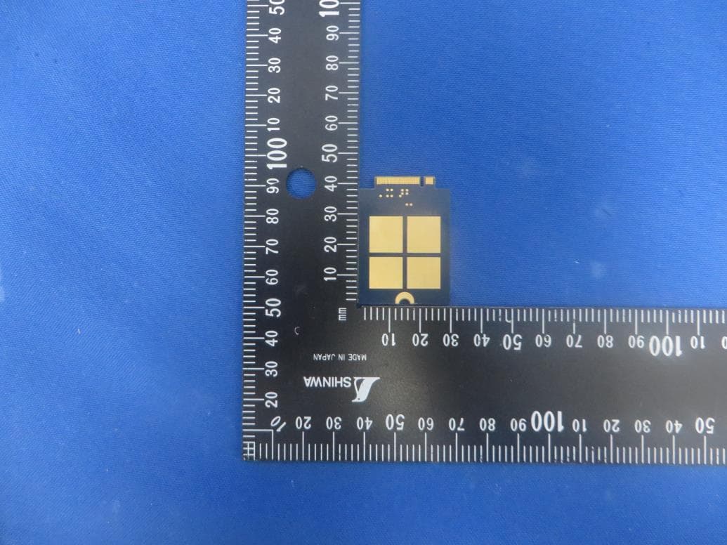
Click to zoom
Application Details
- Equipment Class
- CBE - Citizens Band End User Devices
- Date of Grant
- Jul 18, 2023
- Application Purpose
- Original Equipment
- Date of Application
- Jul 15, 2023
- Equipment Note
- LTE-A Cat 16 M.2 Module
- Frequency Range
- 3552.50000000 - 3697.50000000
- Country
- China
Documents & Files
Document Text
Text extracted from the exhibit documents filed with the FCC. Open a document above to read the original.
Users Manual
EM120R-GL&EM160R-GL Hardware Design LTE-A Module Series Rev. EM120R-GL&EM160R-GL_Hardware_Design_V1.0 Date: 2020-07-02 Status: Preliminary www.quectel.com LTE-A Module Series EM120R-GL&EM160R-GL Hardware Design EM120R-GL&EM160R-GL_Hardware_Design 1 / 79 Our aim is to provide customers with timely and comprehensive service. For any assistance, please contact our company headquarters: Quectel Wireless Solutions Co., Ltd. Building 5, Shanghai Business Park Phase III (Area B), No.1016 Tianlin Road, Minhang District, Shanghai 200233, China Tel: +86 21 5108 6236 Email: [email protected] Or our local office. For more information, please visit: http://www.quectel.com/support/sales.htm For technical support, or to report documentation errors, please visit: http://www.quectel.com/support/technical.htm Or email to: [email protected] GENERAL NOTES QUECTEL OFFERS THE INFORMATION AS A SERVICE TO ITS CUSTOMERS. THE INFORMATION PROVIDED IS BASED UPON CUSTOMERS’ REQUIREMENTS. QUECTEL MAKES EVERY EFFORT TO ENSURE THE QUALITY OF THE INFORMATION IT MAKES AVAILABLE. QUECTEL DOES NOT MAKE ANY WARRANTY AS TO THE INFORMATION CONTAINED HEREIN, AND DOES NOT ACCEPT ANY LIABILITY FOR ANY INJURY, LOSS OR DAMAGE OF ANY KIND INCURRED BY USE OF OR RELIANCE UPON THE INFORMATION. ALL INFORMATION SUPPLIED HEREIN IS SUBJECT TO CHANGE WITHOUT PRIOR NOTICE. COPYRIGHT THE INFORMATION CONTAINED HERE IS PROPRIETARY TECHNICAL INFORMATION OF QUECTEL WIRELESS SOLUTIONS CO., LTD. TRANSMITTING, REPRODUCTION, DISSEMINATION AND EDITING OF THIS DOCUMENT AS WELL AS UTILIZATION OF THE CONTENT WITHOUT PERMISSION ARE FORBIDDEN. OFFENDERS WILL BE HELD LIABLE FOR PAYMENT OF DAMAGES. ALL RIGHTS ARE RESERVED IN THE EVENT OF A PATENT GRANT OR REGISTRATION OF A UTILITY MODEL OR DESIGN. Copyright © Quectel Wireless Solutions Co., Ltd. 2020. All rights reserved. LTE-A Module Series EM120R-GL&EM160R-GL Hardware Design EM120R-GL&EM160R-GL_Hardware_Design 2 / 79 About the Document Revision History Version Date Author Description 1.0 2020-07-02 Jim HAN/ Charls SHENG Initial LTE-A Module Series EM120R-GL&EM160R-GL Hardware Design EM120R-GL&EM160R-GL_Hardware_Design 3 / 79 Contents About the Document ................................................................................................................................... 2 Contents ....................................................................................................................................................... 3 Table Index ................................................................................................................................................... 5 Figure Index ................................................................................................................................................. 7 1 Introduction .......................................................................................................................................... 9 1.1. Safety Information ..................................................................................................................... 10 2 Product Concept ................................................................................................................................ 11 2.1. General Description .................................................................................................................. 11 2.2. Key Features ............................................................................................................................. 12 2.3. Functional Diagram ................................................................................................................... 14 2.4. Evaluation Board ....................................................................................................................... 15 3 Application Interfaces........................................................................................................................ 16 3.1. Pin Assignment ......................................................................................................................... 17 3.2. Pin Description .......................................................................................................................... 18 3.3. Power Supply ............................................................................................................................ 23 3.3.1. Decrease Voltage Drop .................................................................................................. 23 3.3.2. Reference Design for Power Supply.............................................................................. 24 3.4. Turn-on and Turn-off Scenarios ................................................................................................ 25 3.4.1. Turn on the Module ........................................................................................................ 25 3.4.1.1. Turn on the Module with a Host GPIO ................................................................ 25 3.4.1.2. Turn on the Module Automatically ....................................................................... 26 3.4.1.3. Turn on the Module with Compatible Design ...................................................... 26 3.4.2. Turn off the Module ........................................................................................................ 28 3.4.2.1. Turn off the Module through FULL_CARD_POWER_OFF#............................... 28 3.4.2.2. Turn off the Module through AT Command ......................................................... 28 3.5. Reset ......................................................................................................................................... 30 3.6. (U)SIM Interfaces ...................................................................................................................... 32 3.7. USB Interface .............................................................................…
Text truncated - open the document above for the full version.
Cover Letter(s)
Federal Communications Commission 7435 Oakland MiUs Road Colum创aMD 21046 在lUECTE4ι Subject: Certifi田t10ndøsignating a U.8. agent for servJce of pro佣目pursuantto Part 2.911(d)(7) Towhom忧may∞ncem, Quectel Wireless Solutlons Company limited, Grantee Code: XMR ("the appllcant可回而霄esthat, as of the date 01 the filing of app四tion,lk。国kUSA,I时IFRN: 003335033唱('theagent可isdesignated as the U.S. agent fOf the pu巾。seofa∞epting service of process on behalf of the appli四川 The phys也alU.5 . address and email 10r the designaled agent are Physical U .8. addr&幽9920Pac而cHeights Blvd., Ste. 150, #7025, San四吨。,CA92121 Email: ∞mpliance@ikotek..∞m The appticant ac回回sto maintain an agent fOf service of process in the United States for no les$ than one year after either the grantee has permane川Iyterminaled all ma毗etìngand阳p。由tion01 the appl四bleequipment 恻thinthe U.S., or the conclusion 01 any Commission.related administrative or judicial proceeding involving the eqUlpmen忧,whichever Is later. The agent ac国ptsthe designation by (the applicant) as the U.S. agent to accept service 01 pr田essincludes, oot Is not limited to, d创i晴ryof any∞rresponden出,notices, orders, decisions, and陪quirements01 administrative , legal, or judicial process related to Commission pro晤时Ings Signed by the Applicant Email: [email protected] Date: 16 Februa叩2023 Signed by the Agent (i1 d汗1erentfrom the Applicant) rF二7"""'::可-、 、、J一-' ~町百二酬M.Peterson Trtle: President and CE。 Email; joe.pete陌[email protected] Date: Feb阳ary17 th , 2023
Cover Letter(s)
Quectel Wireless Solutions Company Limited Building 5, Shanghai Business Park Phase III (Area B), No.1016 Tianlin Road, Minhang District, Shanghai, China 200233 070920-02b Request for Modular/Limited Modular Approval Date: July 19, 2023 Subject: Manufacturer’s Declaration for ☒ - Modular Approval ☐ - Split Modular Approval ☐ - Limited Modular Approval ☐ - Limited Split Modular Approval Confidentiality Request for: XMR2023EM160RGL 8 Basic Requirements – FCC Part 15.212(a)(1) For Items Marked “NO(*)”, the Limited Module Description Must be Filled Out on the Following Pages Modular Approval Requirement Requirement Met 1. The modular transmitter must have its own RF shielding. This is intended to ensure that the module does not have to rely upon the shielding provided by the device into which it is installed in order for all modular transmitter emissions to comply with FCC limits. It is also intended to prevent coupling between the RF circuitry of the module and any wires or circuits in the device into which the module is installed. Such coupling may result in non-compliant operation. The physical crystal and tuning capacitors may be located external to the shielded radio elements. 15.212(a)(1)(i) ☒ - YES ☐ - NO(*) Details: <example – The module contains a metal shield which covers all RF components and circuitry. The shield is located on the top of the board next to antenna connector> 2. The modular transmitter must have buffered modulation/data inputs (if such inputs are provided) to ensure that the module will comply with FCC requirements under conditions of excessive data rates or over-modulation. 15.212(a)(1)(ii) ☒ - YES ☐ - NO(*) Details: <example – Data to the modulation circuit is buffered as described in the operational description provided with the application> 3. The modular transmitter must have its own power supply regulation on the module. This is intended to ensure that the module will comply with FCC requirements regardless of the design of the power supplying circuitry in the device into which the module is installed. 15.212(a)(1)(iii) ☒ - YES ☐ - NO(*) Details: <example – The module contains its own power supply regulation. Please refer to schematic filed with this application> 4. The modular transmitter must comply with the antenna and transmission system requirements of §§ 15.203, 15.204(b), 15.204(c), 15.212(a), and 2.929(b). The antenna must either be permanently attached or employ a ‘‘unique’’ antenna coupler (at all connections between the module and the antenna, including the cable). The ‘‘professional installation’’ provision of § 15.203 is not applicable to modules but can apply to limited modular approvals under paragraph 15.212(b). 15.212(a)(1)(iv) ☒ - YES ☐ - NO(*) Details: <example – The module connects to its antenna using an UFL connector which is considered a non-standard connector. A list of antennas tested and approved with this device may be found in users manual provided with the application> 5. The modular transmitter must be tested in a stand-alone configuration, i.e., the module must not be inside another device during testing. This is intended to demonstrate that the module is capable of complying with Part 15 emission limits regardless of the device into which it is eventually installed. Unless the transmitter module will be battery powered, it must comply with the AC line conducted requirements found in Section 15.207. AC or DC power lines and data input/output lines connected to the module must not contain ferrites, unless they will be marketed with the module (see Section 15.27(a)). The length of these lines shall be length typical of actual use or, if that length is unknown, at least 10 centimeters to insure that there is no coupling between the case of the module and supporting equipment. Any accessories, peripherals, or support equipment connected to the module during testing shall be unmodified or commercially available (see Section 15.31(i)). 15.212(a)(1)(v) ☒ - YES ☐ - NO(*) Details: <example – The module was tested stand-alone as shown in test setup photographs filed with this application> Quectel Wireless Solutions Company Limited Building 5, Shanghai Business Park Phase III (Area B), No.1016 Tianlin Road, Minhang District, Shanghai, China 200233 070920-02b Modular Approval Requirement Requirement Met 6. The modular transmitter must be labeled with its own FCC ID number, or use an electron display (see KDB Publication 784748). If using a permanently affixed label with its own FCC ID number, if the FCC ID is not visible when the module is installed inside another device, then the outside of the device into which the module is installed must also display a label referring to the enclosed module. This exterior label can use wording such as the following: “Contains Transmitter Module FCC ID: XYZMODEL1” or “Contains FCC ID: XYZMODEL1.” Any similar wording that expresses the same meaning may be used. The Grantee may either provide such a label, an example of which must be included in the application for equipment authorization, or, must provide adequate instructions along with the module which explain this requirement. In the latter case, a copy of these instructions must be included in the application for equipment authorization. If the modular transmitter uses an electronic display of the FCC identification number, the information must be readily accessible and visible on the modular transmitter or on the device in which it is installed. If the module is installed inside another device, then the outside of the device into which the module is installed must display a label referring to the enclosed module. This exterior label can use wording such as the following: “Contains FCC certified transmitter module(s).” Any similar wording that expresses the same meaning may be used. The user manual must include instructions on how to access the electronic display. A copy of these instructions must be included in the application for equipment authoriza…
Text truncated - open the document above for the full version.
External Photos
Report No.: 2306RSU048-UE 1 of 2 EUT Photograph (1) EUT Photo (2) EUT Photo Report No.: 2306RSU048-UE 2 of 2 (3) EUT Photo
ID Label/Location Info
Label Location
Internal Photos
Report No.: 2306RSU048-UE 1 of 2 EUT Photograph (1) EUT Photo (2) EUT Photo Report No.: 2306RSU048-UE 2 of 2 (3) EUT Photo
RF Exposure Info
MRT Technology (Suzhou) Co., Ltd Report No.: 2306RSU048-U13 Phone: +86-512-66308358 Report Version: V01 Web: www.mrt-cert.com Issue Date: 2023-07-14 Template Version:0.0 1 of 11 RF Exposure Evaluation Declaration FCC ID: XMR2023EM160RGL Applicant: Quectel Wireless Solutions Co., Ltd Product: LTE-A Cat 16 M.2 Module Model No.: EM160R-GL Brand Name: Quectel FCC Rule Part(s): FCC Part 2.1091 Result: Complies Reviewed By: Sunny Sun Approved By: Robin Wu The test results relate only to the samples tested. The test results shown in the test report are traceable to the national/international standards through the calibration of the equipment and evaluated measurement uncertainty herein. The test report shall not be reproduced except in full without the written approval of MRT Technology (Suzhou) Co., Ltd. Report No.: 2306RSU048-U13 2 of 11 Revision History Report No. Version Description Issue Date Note 2306RSU048-U13 Rev. 01 Initial Report 2023-07-14 Valid Report No.: 2306RSU048-U13 3 of 11 CONTENTS Description Page 1. General Information ................................................................................................................................ 4 1.1. Applicant ........................................................................................................................................ 4 1.2. Manufacturer ................................................................................................................................. 4 1.3. Testing Facility ............................................................................................................................... 4 1.4. Product Information ....................................................................................................................... 5 1.5. Description of Available Antennas ................................................................................................. 6 1.6. Applied Standards ......................................................................................................................... 6 2. RF Exposure Evaluation ......................................................................................................................... 7 2.1. Test Limits ..................................................................................................................................... 7 2.2. MPE Exemptions ........................................................................................................................... 8 2.3. Device Classification ................................................................................................................... 10 2.4. Calculated Result ......................................................................................................................... 11 Report No.: 2306RSU048-U13 4 of 11 1. General Information 1.1. Applicant Quectel Wireless Solutions Co., Ltd Building 5, Shanghai Business Park Phase III (Area B), No.1016 Tianlin Road, Minhang District, Shanghai, China 200233 1.2. Manufacturer Quectel Wireless Solutions Co., Ltd Building 5, Shanghai Business Park Phase III (Area B), No.1016 Tianlin Road, Minhang District, Shanghai, China 200233 1.3. Testing Facility Test Site – MRT Suzhou Laboratory Laboratory Location (Suzhou - Wuzhong) D8 Building, No.2 Tian’edang Rd., Wuzhong Economic Development Zone, Suzhou, China Laboratory Location (Suzhou - SIP) 4b Building, Liando U Valley, No.200 Xingpu Rd., Shengpu Town, Suzhou Industrial Park, China Laboratory Accreditations A2LA: 3628.01 CNAS: L10551 FCC: CN1166 ISED: CN0001 VCCI: R-20025 G-20034 C-20020 T-20020 R-20141 G-20134 C-20103 T-20104 Test Site – MRT Shenzhen Laboratory Laboratory Location (Shenzhen) 1G, Building A, Junxiangda Building, Zhongshanyuan Road West, Nanshan District, Shenzhen, China Laboratory Accreditations A2LA: 3628.02 CNAS: L10551 FCC: CN1284 ISED: CN0105 Test Site – MRT Taiwan Laboratory Laboratory Location (Taiwan) No. 38, Fuxing 2nd Rd., Guishan Dist., Taoyuan City 333, Taiwan (R.O.C.) Laboratory Accreditations TAF: L3261-190725 FCC: 291082, TW3261 ISED: TW3261 Report No.: 2306RSU048-U13 5 of 11 1.4. Product Information Product Name: LTE-A Cat 16 M.2 Module Model No.: EM160R-GL Brand Name: Quectel IMEI: 86292050003514 WCDMA Band: Band II, Band IV, Band V Single Band: Band 2, 4, 5, 7, 12, 13, 14, 25, 26, 30, 38, 41, 48, 66 Intra-Band: CA_41C Category: Category 16 Operating Temperature: -25 ~ 75 °C Power Type: 3.1 ~ 4.4Vdc, typical 3.7Vdc Remark: The declared of product specification for EUT presented in the report are provided by the manufacturer, and the manufacturer takes all the responsibilities for the accuracy of product specification. Report No.: 2306RSU048-U13 6 of 11 1.5. Description of Available Antennas Technology Frequency Range (MHz) Antenna Type Max Peak Gain (dBi) WCDMA & LTE Band 2 1850 ~ 1910 Dipole 1.15 WCDMA & LTE Band 4 1710 ~ 1755 -0.50 WCDMA & LTE Band 5 824 ~ 849 1.85 LTE Band 7 2500 ~ 2570 1.32 LTE Band 12 699 ~ 716 -2.43 LTE Band 13 777 ~ 787 -0.10 LTE Band 14 788 ~ 798 2.40 LTE Band 25 1850 ~ 1915 1.15 LTE Band 26 814 ~ 849 1.85 LTE Band 30 2305 ~ 2315 -3.64 LTE Band 38 2570 ~ 2620 0.93 LTE Band 41 2496 ~ 2690 0.93 LTE Band 48 3550 ~ 3700 -3.37 LTE Band 66 1710 ~ 1780 -0.50 Note: All antenna information (Antenna type and Peak Gain) is provided by the manufacturer. 1.6. Applied Standards According to the specifications of the manufacturer, the EUT must comply with the requirements of the following standards: ⚫ FCC Part 2.1091 & KDB 447498 D04 Interim General RF Exposure Guidance v01 Report No.: 2306RSU048-U13 7 of 11 2. RF Exposure Evaluation 2.1. Test Limits According to FCC §1.1310: The criteria listed in the following table shall be used to evaluate the environment impact of human exposure to radio frequency (RF) radiation as specified in §1.1307(b) Limits For Maximum Permissible Exposure (MPE) Frequency Range (MHz) Electric Field Strength (V/m) Magnetic Field Strength (A/m) Power …
Text truncated - open the document above for the full version.
Test Report
MRT Technology (Suzhou) Co., Ltd Report No.: 2306RSU048-U1 Phone: +86-512-66308358 Report Version: V01 Web: www.mrt-cert.com Issue Date: 2023-07-14 1 of 45 MEASUREMENT REPORT FCC ID: XMR2023EM160RGL Application: Quectel Wireless Solutions Co., Ltd Product: LTE-A Cat 16 M.2 Module Model No.: EM160R-GL Brand Name: QUECTEL FCC Rule Part(s): Part 2, 96 Result: Complies Test Date: 2020-06-19 ~ 2020-08-15 Reviewed By: Sunny Sun Approved By: Robin Wu The test results relate only to the samples tested. This equipment has been shown to be capable of compliance with the applicable technical standards as indicated in the measurement report and was tested in accordance with the measurement procedures specified in ANSI C63.26-2015. Test results reported herein relate only to the item(s) tested. The test report shall not be reproduced except in full without the written approval of MRT Technology (Suzhou) Co., Ltd. Report No.: 2306RSU048-U1 2 of 45 Revision History Report No. Version Description Issue Date Note 2306RSU048-U1 Rev. 01 Initial Report 2023-07-14 Valid Note: This report is based on MRT report “2009RSU020”, FCC ID: XMR2020EM160RGL updating FCC ID. Report No.: 2306RSU048-U1 3 of 45 CONTENTS Description Page 1. GENERAL INFORMATION ...................................................................................................... 5 1.1. Applicant ...................................................................................................................... 5 1.2. Manufacturer ................................................................................................................ 5 1.3. Testing Facility .............................................................................................................. 5 2. PRODUCT INFORMATION ...................................................................................................... 6 2.1. Equipment Description ................................................................................................. 6 2.2. Product Specification Subjective to this Report ............................................................ 6 2.3. Description of Available Antennas ................................................................................. 7 2.4. EMI Suppression Device(s)/Modifications ..................................................................... 7 2.5. Maximum Power, Frequency Tolerance, and Emission Designator .............................. 7 2.6. Configuration of Tested System ................................................................................... 8 2.7. Test Environment Condition .......................................................................................... 8 3. TEST EQUIPMENT CALIBRATION DATE ............................................................................... 9 4. MEASUREMENT UNCERTAINTY ......................................................................................... 11 5. TEST RESULT ....................................................................................................................... 12 5.1. Summary .................................................................................................................... 12 5.2. Occupied Bandwidth .................................................................................................. 13 5.2.1. Test Limit ................................................................................................................ 13 5.2.2. Test Procedure ....................................................................................................... 13 5.2.3. Test Setting ............................................................................................................. 13 5.2.4. Test Setup .............................................................................................................. 13 5.2.5. Test Result .............................................................................................................. 14 5.3. Frequency Stability Measurement .............................................................................. 17 5.3.1. Test Limit ................................................................................................................ 17 5.3.2. Test Procedures Used ............................................................................................ 17 5.3.3. Test Setting ............................................................................................................. 17 5.3.4. Test Setup .............................................................................................................. 18 5.3.5. Test Result .............................................................................................................. 19 5.4. Equivalent Isotropically Radiated Power Measurement .............................................. 20 5.4.1. Test Limit ................................................................................................................ 20 5.4.2. Test Procedures Used ............................................................................................ 20 5.4.3. Test Setting ............................................................................................................. 20 5.4.4. Test Setup .............................................................................................................. 21 5.4.5. Test Result .............................................................................................................. 22 Report No.: 2306RSU048-U1 4 of 45 5.5. Band Edge Measurement ........................................................................................... 24 5.5.1. Test Limit ................................................................................................................ 24 5.5.2. Test Procedure Used .............................................................................................. 24 5.5.3. Test Setting ......................…
Text truncated - open the document above for the full version.
Test Report
Report No.: 2306RSU048-U1 31 of 45 5MHz Channel Bandwidth – Full RB Low Channel ACP Extended Band Edge Extended Band Edge Middle Channel ACP Extended Band Edge Extended Band Edge High Channel ACP Extended Band Edge Report No.: 2306RSU048-U1 32 of 45 10MHz Channel Bandwidth – Full RB Low Channel ACP Middle Channel ACP High Channel ACP Report No.: 2306RSU048-U1 33 of 45 15MHz Channel Bandwidth – Full RB Low Channel ACP Middle Channel ACP High Channel ACP Report No.: 2306RSU048-U1 34 of 45 20MHz Channel Bandwidth – Full RB Low Channel ACP Middle Channel ACP High Channel ACP Report No.: 2306RSU048-U1 35 of 45 5.6. Conducted Spurious Emissions 5.6.1.Test Limit The level of the carrier and the various conducted spurious and harmonic frequencies is measured by means of a calibrated spectrum analyzer. The spectrum is scanned from the lowest frequency generated in the equipment up to a frequency including its 10 th harmonic. All out of band emissions are measured with a spectrum analyzer connected to the antenna terminal of the EUT while the EUT is operating at its maximum duty cycle, at maximum power, and at the appropriate frequencies. All data rates were investigated to determine the worst-case configuration. All modes of operation were investigated, and the worst-case configuration results are reported in this section. The conducted power of any emissions below 3530MHz or above 3720MHz shall not exceed -40dBm/MHz. 5.6.2.Test Procedure Used ANSI C63.26-2015 - Section 5.7 5.6.3.Test Setting 1. Set the analyzer frequency to low, mid, high channel. 2. RBW = 1MHz 3. VBW ≥ 3*RBW 4. Sweep time = auto 5. Detector = power averaging (rms) 6. Set sweep trigger to “free run.” 7. User gate triggered such that the analyzer only sweeps when the device is transmitting at full power. 8. Trace average at least 100 traces in power averaging (rms) mode if sweep is set to auto-couple. To accurately determine the average power over the on and off time of the transmitter, it can be necessary to increase the number of traces to be averaged above 100, or if using a manually configured sweep time, increase the sweep time. Report No.: 2306RSU048-U1 36 of 45 5.6.4.Test Setup Report No.: 2306RSU048-U1 37 of 45 5.6.5.Test Result Product LTE-A Cat 16 M.2 Module Temperature 25°C Test Engineer Candy Luo Relative Humidity 54% Test Site TR3 Test Date 2020/07/13 Channel Frequency (MHz) Channel Bandwidth (MHz) Frequency Range (MHz) Max Spurious Emissions (dBm/MHz) Limit (dBm/ MHz) Result QPSK 55265 3552.5 5 30 ~ 40000 -47.21 ≤ -40.00 Pass 55900 3625.0 5 30 ~ 40000 -53.51 ≤ -40.00 Pass 56715 3697.5 5 30 ~ 40000 -51.72 ≤ -40.00 Pass 55290 3555.0 10 30 ~ 40000 -52.77 ≤ -40.00 Pass 55900 3625.0 10 30 ~ 40000 -50.71 ≤ -40.00 Pass 56690 3695.0 10 30 ~ 40000 -53.84 ≤ -40.00 Pass 55315 3557.5 15 30 ~ 40000 -50.67 ≤ -40.00 Pass 55900 3625.0 15 30 ~ 40000 -53.02 ≤ -40.00 Pass 56665 3692.5 15 30 ~ 40000 -49.28 ≤ -40.00 Pass 55340 3550.0 20 30 ~ 40000 -51.61 ≤ -40.00 Pass 55900 3625.0 20 30 ~ 40000 -52.39 ≤ -40.00 Pass 56640 3690.0 20 30 ~ 40000 -49.22 ≤ -40.00 Pass Report No.: 2306RSU048-U1 38 of 45 5MHz Channel Bandwidth Channel 55265 (3552.5MHz) Channel 55900 (3625.0MHz) Channel 56715 (3697.5MHz) 10MHz Channel Bandwidth Channel 55290 (3555.0MHz) Channel 55900 (3625.0MHz) Channel 56690 (3695.0Hz) Report No.: 2306RSU048-U1 39 of 45 15MHz Channel Bandwidth Channel 55315 (3557.5MHz) Channel 55900 (3625.0MHz) Channel 56665 (3692.5Hz) 20MHz Channel Bandwidth Channel 55340 (3550.0MHz) Channel 38000 (3625.0MHz) Channel 56640(3690.0MHz) Report No.: 2306RSU048-U1 40 of 45 5.7. End User Device Additional Requirement (CBSD Protocol) 5.7.1.Test Limit End User Devices may operate only if they can positively receive and decode an authorization signal transmitted by a CBSD, including the frequencies and power limits for their operation. An End User Device must discontinue operations, change frequencies, or change its operational power level within 10 seconds of receiving instructions from its associated CBSD 5.7.2.Test Procedure Used KDB 940660 D01 v02, WINNF-TS-0122 V1.0.0 5.7.3.Test Setting The EUT was connected via an RF cable to a certified CBSD (Ruckus Wireless, Inc. FCC ID: S9GQ910US00) and spectrum analyzer. The following proc…
Text truncated - open the document above for the full version.
Contact Information
Applicant
Jean Hu
Technical Contact
MRT Technology (Suzhou) Co., LtdMarlin Chen
[email protected]86-512-66308358
D8 Building, Youxin Industrial Park, · Suzhou · China
Non-Technical Contact
MRT Technology (Suzhou) Co., LtdMarlin Chen
[email protected]86-512-66308358
Test Firm
MRT Technology (Suzhou) Co., Ltd.Mr. Marlin Chen
[email protected]8651266308358
Technical Specifications
| # | Rule Parts | Frequency Range | Power Output | Emission | Tolerance |
|---|---|---|---|---|---|
| 3 | 96 | 3.55 GHz - 3.70 GHz | 92.50 mW | 4M46G7D | 0.0028 ppm |
Other Applications from Quectel Wireless Solutions Company Limited
XMR2026FME160X
Sep 11, 2026Wi-Fi & Bluetooth Module
Equipment Class
DSS - Part 15 Spread Spectrum TransmitterXMR2026FCE860X
Sep 11, 2026Wi-Fi & Bluetooth Module
Equipment Class
NII - Unlicensed National Information Infrastructure TXXMRFCH100XH915
Sep 10, 2026Wi-Fi HaLow Module
Equipment Class
DTS - Digital Transmission SystemXMR2026RG255GNA
Sep 04, 20265G RedCap Sub-6 GHz Module
Equipment Class
CBE - Citizens Band End User DevicesXMR2026KGM100XB
Aug 28, 2026Wireless Module for Amazon Sidewalk
Equipment Class
DTS - Digital Transmission System