Y4GCU560-1Two Way Radio
SHENZHEN COVALUE COMMUNICATIONS CO., LTD.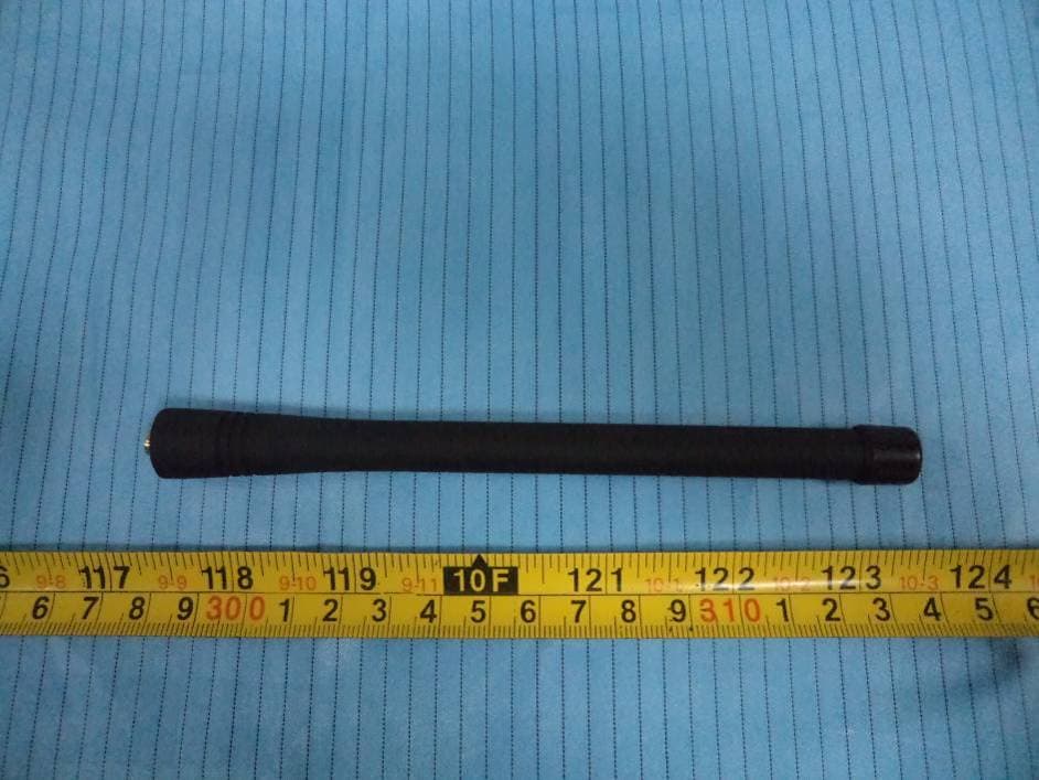
Click to zoom
Application Details
- Equipment Class
- TNF - Licensed Non-Broadcast Transmitter Held to Face
- Date of Grant
- Mar 28, 2013
- Application Purpose
- Original Equipment
- Date of Application
- Mar 28, 2013
- Equipment Note
- Two Way Radio
- Frequency Range
- 136.00000000 - 174.00000000
- Country
- China
Documents & Files
Document Text
Text extracted from the exhibit documents filed with the FCC. Open a document above to read the original.
Users Manual
Instruction Manual CU560-1 FM Portable Radio Thank you for purc hasing a COVALUE two-way radio. This simple to use radio adopts the latest advances in technology, providing reliable communication in today’s demanding communication environment. Notice to the User: · Please read this instruction manual before operating this radio. · It’s prohibited to use the radio or charge it at any area with a potentially explosive atmosphere (where the air contains gas, dust and smog, etc.), as well as while taking on fuel, or while parking at a gasoline service station; or any area where radio communication is prohibited (such as a hospital or a airport.) · It’s prohibited to operate the radio without permission in areas where the government laws prohibit radio communication. · Please don't expose the radio to direct sunlight for a long time; don't place the radio near any heating devices, either. · Please don't put the radio in extremely dusty, moist humid areas or unstable surfaces. · Only qualified personal, with proper tools and instruments are allowed to service and repair the radios, do not disassemble the radio by yourself to avoid damages. Warning: Your radio g enerates RF electromagnetic energy during transmit mode. This radio is designed for and classified as "ccupational Use Only" meaning it must be used only during the course of employment by individuals aware of the hazards, and the ways to minimize such hazards. This radio is NOT intended for use by the "eneral Population"in an uncontrolled environment. This radio has been tested and complies with the FCC RF exposure limits for "ccupational Use Only" In addition, your SHENZHEN COVALUE COMMUNICATIONS CO.,LTD.radio complies with the following Standards and Guidelines with regard to RF energy and electromagnetic energy levels and evaluation of such levels for exposure to humans: 1. FCC OET Bulletin 65 Edition 97-01 Supplement C, Evaluating Compliance with FCC Guidelines for Human Exposure to Radio Frequency Electromagnetic Fields. 2. American National Standards Institute (C95.1-1992), IEEE Standard for Safety Levels with Respect to Human Exposure to Radio Frequency Electromagnetic Fields, 3 kHz to 300 GHz. 3. American National Standards Institute (C95.3-1992), IEEE Recommended Practice for the Measurement of Potentially Hazardous Electromagnetic Fields- RF and Microwave. SHENZ HEN COVALUE COMMUNICATIONS CO., LTD. 4. The following accessories are authorized for use with this product. Use of accessories other than those (listed in the instruction) specified may result in RF exposure levels exceed the FCC requirements for wireless RF exposure. To ensure that your expose to RF electromagnetic energy is within the FCC allowable limits for occupational use, always adhere to the following guidelines: 1. DO NOT operate the radio without a proper antenna attached, as this may damaged the radio and may also cause you to exceed FCC RF exposure limits. A proper antenna is the antenna supplied with this radio by the manufacturer or antenna specifically authorized by the manufacturer for use with this radio. 2. DO NOT transmits for more than 50% of total radio use time (“50% duty cycle”). Transmitting more than 50% of the time can cause FCC RF exposure compliance requirements to be exceeded. The radio is transmitting when the “TX indicator” lights red. You can cause the radio to transmit by pressing the “PTT” switch. 3. ALWAYS keep the antenna at least 2.5 cm (1 inch) away from the body when transmitting and only use the COVALUE belt-clip which is listed in instructions when attaching the radio to your belt, etc., to ensure FCC RF exposure compliance requirements are not exceeded. To provide the recipients of your transmission the best sound quality, hold the antenna at least 5 cm (2 inches) from your mouth, and slightly off to one side. The information listed above provides the user with the information needed to make him or her aware of RF exposure, and what to do to as*sure that this radio operates with the FCC RF exposure limits of this radio. Electromagnetic Interference/Compatibility During transmissions, your COVALUE radio generates RF energy that can possibly cause interference with other devices or systems. To avoid such interference, turn off the radio in areas where signs are posted to do so. DO NOT operate the transmitter in areas that are sensitive to electromagnetic radiation such as hospitals, aircraft, and blasting sites. Occupational/Controlled Use The radio transmitter is used in situations in which persons are exposed as consequence of their employment provided those persons are fully aware of the potential for exposure and can exercise control over their exposure. IC RF exposure statement: The device meets the exemption from the rout ine evaluation limits in section 2.5 of RSS 102 RF exposure,users can obtain Canadian information on RF exposure and compliance. IC RF exposure statement:IC RF exposure statement:IC RF exposure statement: CONTENTS ■ Unpacking and Checking the Equipment ------------------------------------ Supplied Accessories---------------------------------------------------- ■ Preparation ----------------------------------------------------------- Charging the Battery Installing/Removing the Battery Pack Installing the Antenna Installing the Optional Speaker/Microphone Installing/Removing the Belt Clip ■ Radio Overview ■ Basic Operations ■ Programmable Button Function ■ VOX (Voice Operated Transmission) ■ Radio Setting TOT (Time-out Timer) Battery Save Low Power Warning Channel Annunciation CTCSS/DCS ■ User Template RX Squelch Mode DTMF 5-Tone Signaling 2-Tone Signaling MDC Signaling ■ Troubleshooting ■ Major Specifications ■ Settings ■ Unpacking and Checking the Equipment Unpack the radio carefully. We recommend that you identify the items listed in the following table before discarding the packing material. If any items are missing or have been damaged during shipment, please contact the carrier or the dealer immediat…
Text truncated - open the document above for the full version.
Block Diagram
1 2 3 4 5 6 78 ABCD 8 7 6 5 4 3 2 1 D CBA ANT LPF Q11RD07 D1 HVU131 RF AMP ANT SW Q12 2SK3475 RF AMP Q3 2SC3356 RF AMP Q42SC5066 RF AMP 12.8MHz LPF QTTCXO DET Q168 DTC144EE DCSW APCSW CURRENT IC3 NJM2904V B APC IC8XC6201P502MR Q29FMMT717 3TC IC7XC6201P332MR 3M Q8ST2302 Q23 DTC114EE MUTE DC SW SW IC1TDA2822D AF D29 GREEN AMP LED Q33DTC144EE DCSW Q37DTC144EEDCSW Q8 FMMT717 DCSW Batt Det PROTECT Q22 DTC114EE DC SW D28 RED LED IC401 FLASH X29.8304MHz Q28 DTC144EE SW + - LOBATT BATT PWR SW / VOL SP MIC EXT SW SB SB AFCO 5T 5T PTTKEYUPKEYDOWNKEYALARM SB SB RLED GLED IC2 MICROPROCESSOR BSHIFT XOUT XIN 3M RESETVOXInRXD RDApDn LOBATT ECO4ECO6 PTTkEYDOWnkEYUpkEYALARM 3TCTXDAFCOAPCSW SAVEAPC DTMFRLEDGLED IC901 TA75W01FU COMP Q5022SC4617 AMP Q508 2SC4617 AMP 5M 5M VOXIn 5R SB IC300B IC300A LPF MOD IC300C HPF IC300D HPF NJM2902V 5R 5R 5R 5R 136-174MHz CU560-1 BLOCK DIAGRAM VER 1.0 TitleSize A3 Number Revision Date:File: Sheet ofDrawn By: RDA1846 RDAGpIO5RDAEnRDADATARDACLk SQL AF MUTE 2T/5TIn 2T/5TIn SB 5R5T CTC/DCSIn CTC/DCSOUT IC5 ECO6 CH SW ECO1ECO2ECO4GND ECO1ECO3 Q AFOUT I RFOUT RFIN I PGA ... PDN DVDD I2C GPIO7 VCO Q GPIO0 SPI AFC loop FM modem Bus Sub CH filter Core RSSI Audio filter DSP Synthesizer Interface ADC GPIO PGA LDO ADC ADC DAC PA_driver MIC AVDD Q/90 XTAL ≈ + - 3M RDAInT RDAGpIO4
External Photos
EXHIBIT B - EUT EXTERNAL PHOTOGRAPHS EUT with Antenna View EUT – Front View EUT – Rear View EUT – Top without Antenna View EUT – Bottom View EUT – Left Side View EUT – Right Side View EUT – Antenna View
ID Label/Location Info
EXHIBIT A - FCC ID LABELING AND LOCATION FCC ID Label Statement FCC ID Label Location The label shown shall be permanently affixed at a conspicuous location on the device and be readily visible to the user at the time purchase (Labeling requirements per 2.925) Statement Label Here
Internal Photos
EXHIBIT C - EUT INTERNAL PHOTOGRAPHS EUT – Battery off View EUT – Cover off View 1 EUT – Cover off View 2 EUT – Main Board Top View EUT – Main Board Bottom View EUT – Battery View
Operational Description
1 Circuit Description 1 SINGLE CHIP TRANSCEIVER RDA1846 is one of the main components of the walkie-talkie. The RDA1846 is a highly integrated single-chip transceiver for Walkie Talkie applications. It totally realizes the translation from RF carrier to voice in the RX path and from voice to RF carrier in the TX path, requiring only one micro controller. Figure 1 RDA1846 Block Diagram 2 Receiver (RX) Front end The RX signal from the antenna is passed through the LPF and antenna SW (D1, D4 and D5), and is sent to pin 15 of IC5 (RDA1846) to be demodulated and to output Figure 2 Receiver Diagram 2 Audio signal processing The demodulated audio signal output from IC5 (RDA1846) passes through the volume potentiometer to be adjusted, and then goes to the audio power amplifier IC1 (TDA2822). Squelch circuit Output from pin 26 of IC5 (RDA1846) is sent to the MCU. MCU identifies the level of the noise and controls the squelch. Audio power amplifier The BTL type audio power amplifier circuit consists of IC1 and its peripheral components. Base electrode of Q38 is the control terminal. High level: Open; Low level: Close. The Rx audio signal, voice alert signal, alert tone signal and warning tone signal are collected and passed through the audio power amplifier where they are amplified and output to drive the speaker. The volume of the warning tone is not controlled by the preset volume level of the radio. Speaker impedance: 16Ω. Note: Any terminal of the speaker should not be grounded! CTCSS/DCS signal processing CTCSS/DCS signal output from pin 32 of IC5 (RDA1846) is sent to MCU for decoding. 3 Transmitter (TX) Figure 3 Transmitter Diagram TX power amplification The modulated RF signal from IC5 (RDA1846) is amplified by Q4, Q3 and Q12, and is sent to Q11 for power amplification. Output power of Q11: 5.0W. Grid bias of Q12 and Q11 is controlled by the APC circuit. Through changing the grid bias voltage, the Tx output power can be controlled conveniently. 3 APC (Automatic Power Control) R167, R168 and R169 are used to test the power amplification current. IC3A is the sampling amplifier for the power amplification current. IC3B is the power comparator amplifier. If the Tx output power is too high, the power amplification current and IC3A output will increase; IC3B output voltage will decrease, so the offset voltage added to Q11 and Q12 will also decrease, which causes the Tx output power to be lowered, and vice versa. Thus the Tx output power can keep stable under different working conditions. MCU can set the power through changing the voltage input to IC3B. Tx voice signal processing MIC signal passes through the internal/external MIC switch circuit and is sent to pin 11 of IC5 (RDA1846) for carrier modulation. 4 Frequency Synthesizer The 12.8MHz reference frequency signal provided by X1 is divided by the internal reference frequency divider of IC5 (RDA1846), and is then sent to the internal phase comparator of IC5, where the signal is compared with the signal divided by the fractional frequency divider of internal VCO. Then the output signal is used to control the internal VCO, enabling the frequency to reach the set value. 5 Power Supply The radio uses 7.4V, 1700mAh Li-Poly battery. The Tx power amplification circuit (Q11 and Q12) and the Rx audio power amplifier (IC1) directly adopt the battery for power supply. Power of other circuits is supplied by 5V or 3.3V regulated voltage. IC7:3,3V LDO, 3M power supply, and supplies power for RD1846 and MCU IC8:5V LDO,5R and 5T power supply Q29: 5T switch (controlled by MCU) 5T: supply power for the front end of transmitter 6 MCU Unit MCU Unit controls the operation of every unit to realize all functions of the CU560-2. Communication with external PC State data access Control PLL for the generation, receiving and transmitting of local oscillation frequency Access to the current channel state Control LED status indicator Control power supplied condition of every unit Detect action of every function key Produce CTCSS signal Produce DCS signal Produce power controlled signal Finish CTCSS decoding Finish DCS decoding Squelch detection and control Control voice prompt content 4 Memory (FLASH) Channel data, CTCSS/DCS data and other function setting data and parameter adjustment data. CTCSS/DCS signal coding and decoding: CTCSS/DCS signals from MCU (pin17 output) are sent to pin32 of IC5 for modulation respectively. CTCSS/DCS signals from IC5 are sent to MCU(pin52) for decoding, and then MCU test if there are CTCSS/DCS signals with the same setting of the station to decide whether open the speaker or not. CTCSS (continuous tone control squelch system, hereinafter referred to as CTCSS), is a kind of squelch control system with modulation on carrier and continuous sub-audio signals as pilot tone. If CTCSS function is set, the call is available only at the same CTCSS frequency of both receiving and transmitting parties to avoid the disturbance of other signals. The station has 39 groups of standard CTCSS frequency for your selection, such as Table 1. Table 1 CTCSS Frequency Table No. Frequency [Hz] No. Frequency [Hz] No.Frequency [Hz] No. Frequency [Hz] 1 67.0 11 94.8 21 131.8 31 186.2 2 69.3 12 97.4 22 136.5 32 192.8 3 71.9 13 100.0 23 141.3 33 203.5 4 74.4 14 103.5 24 146.2 34 210.7 5 77.0 15 107.2 25 151.4 35 218.1 6 79.7 16 110.9 26 156.7 36 225.7 7 82.5 17 114.8 27 162.2 37 233.6 8 85.4 18 118.8 28 167.9 38 241.8 9 88.5 19 123.0 29 173.8 39 250.3 10 91.5 20 127.3 30 179.9 DCS signaling: DCS (Digital code squelch), is a kind of continuous digital code modulated on carrier with voice signal and used for squelch control. If DCS function is set, the speaker is available only when receiving the same DCS code to avoid the disturbance of useless signals. The station has 83 kinds of standard codes including positive and inverse code for your selection, such as Table 1 DCS signals produced by MCU (PWM waveform) are sent to IC5 for modulation. CTCSS/DCS signals from receiv…
Text truncated - open the document above for the full version.
Operational Description
Federal Communications CommissionDA 13-431 Before the Federal Communications Commission Washington, D.C. 20554 In the Matter of Implementation of Sections 309(j) and 337 of the Communications Act of 1934 as Amended Promotion of Spectrum Efficient Technologies on Certain Part 90 Frequencies ) ) ) ) ) ) ) WT Docket No. 99-87 RM-9332 ORDER Adopted: March 15, 2013Released: March 18, 2013 By the Chief, Wireless Telecommunications Bureau, Chief, Public Safety and Homeland Security Bureau, and Chief, Office of Engineering and Technology: 1.Introduction.In this Order, we grant in part and deny in part a Petition to Delay Indefinitely Implementation of Section 90.203(j)(5) of the Commission’s Rules filed by Ritron, Inc. (Ritron) on September 21, 2012. 1 Pursuant to Section 90.203(j)(5) of the Commission’s rules, the Commission no longer accepts applications for certification of Part 90 private land mobile radio (PLMR) equipment in the 150-174 MHz and 450-512 MHz bands that cannot operate in a 6.25 kHz mode or with equivalent efficiency. 2 Ritron requests that implementation of this requirement be delayed indefinitely. We conclude that the requirement should be waived only until January 1, 2015. 2.Background.In 1995, the Commission adopted rule changes to promote the efficient use of the PLMR service and facilitate the introduction of advanced technologies. 3 To promote the transition to a more efficient narrowband channel plan, the Commission provided, inter alia, that “only increasingly efficient equipment” would be approved. 4 The Commissiondid not set a date after which it would no longer approve equipment with a wideband (25 kHz) mode, or after which such equipment could no longer be manufactured or used. 5 The Commission contemplated that, as systems reached the end of their service life and new radios were needed, users would migrate to the narrower bandwidth multi-mode radios in order to avoid the adjacent-channel interference that could occur from systems using the adjacent narrowband channels. 6 3.Subsequently, the Commission determined that the 1995 rules failed to provide adequate incentive to realize the Commission’s spectrum efficiency goals in these bands, and stronger measures 1 SeePetition to Delay Indefinitely Implementation Section 90.203(j)(5) of the Commission’s Rules (filed Sept. 21, 2012) (Petition). 2 See47 C.F.R. § 90.203(j)(5). 3 SeeReplacement of Part 90 by Part 88 to Revise the Private Land Mobile Radio Services and Modify the Policies Governing Them, Report and Order and Further Notice of Proposed Rule Making, PR Docket No. 92-235, 10 FCC Rcd 10076, 10077 ¶ 1 (1995). 4 Id.at 10081 ¶ 7. 5 Id.at 10100 ¶ 40. 6 Id. Federal Communications CommissionDA 13-431 2 would be required to bring about a timely transition to narrowband technology. 7 The Commission therefore amended the rules to provide that, by January 1, 2013, Industrial/Business and Public Safety Radio Pool licensees in the 150-174 MHz and 421-512 MHz bands must migrate to 12.5 kHz channel bandwidth or utilize a technology that achieves equivalent efficiency. 8 4.The Commission also adopted interim deadlines to facilitate this transition to narrowband technology. Among other rules, the Commission provided that, beginning January 1, 2011, it would no longer accept applications for certification of equipment that cannot operate in 6.25 kHz mode or with equivalent efficiency. 9 In 2010, the Commission temporarily waived this requirement until January 1, 2013, 10 but stated, “If 6.25 kHz standards still are not in place at that date, interested parties may request a further extension.” 11 5.Ritron, a manufacturer of wireless products, contends that standards for 6.25 kHz technology are not yet in place and that other issues exist that justify delaying implementation of mandatory 6.25 kHz certification by manufacturers.Ritron states that no one 6.25 kHz equipment standard exists and that, in the Industrial/Business sector of the market, two incompatible and proprietary technologies have emerged. 12 Italso argues that 6.25 kHz equipment is still unduly expensive. 13 Finally, Ritron asserts that using the equipment authorization process to facilitate the transition to narrowband technology has been largely unsuccessful. 14 Itconcludes that the implementation of Section 90.203(j)(5) should be delayed until (a) a real need has been established for additional PLMR frequencies beyond those created by the transition to 12.5 kHz channels; (b) the benefits of 6.25 kHz outweigh the associated research and development, manufacturing, and product costs; and (c) a standard has emergedfor a more cost-effective voice compressor/decompressor (vocoder). 15 6.The Wireless Telecommunications Bureau, Public Safety and Homeland Security Bureau and the Office of Engineering and Technology sought comment on Ritron’s request. 16 We asked commenters to address whether the public interest would be served by further delaying implementation of 7 See Implementation of Sections 309(j) and 337 of the Communications Act of 1934 as Amended,Second Report and Order and Second Further Notice of Proposed Rulemaking, WT Docket No. 99-87, 18 FCC Rcd 3034, 3038 ¶ 12 (2003). 8 See 47 C.F.R. § 90.209(b)(5). The January 1, 2013 deadline for converting to 12.5 kHz technology has been waived for licensees in the 470-512 MHz segment of the UHF band (the T-Band). SeeImplementation of Sections 309(j) and 337 of the Communications Act of 1934 as Amended, Order, WT Docket No. 99-87, 27 FCC Rcd 4213 (T-Band Order), on recon., Order on Reconsideration, 27 FCC Rcd 14770 (WTB/PSHSB/OET 2012). 9 See Implementation of Sections 309(j) and 337 of the Communications Act of 1934 as Amended,Third Report and Order, WT Docket No. 99-87, 22 FCC Rcd 6083, 6090 ¶ 16 (2007) (Third Report and Order). 10 See Implementation of Sections 309(j) and 337 of the Communications Act of 1934 as Amended, Order, WT Docket No. 99-87, 25 FCC Rcd 8861, 8866 ¶ 11 (2010) (Order). 11 Id.at 8866 n.41. 12 …
Text truncated - open the document above for the full version.
Parts List/Tune Up Info
1 CU560-1 ADJUSTMENT 1 Required T est Equipment Table 1 Number Name Parameter requirements 1 Computer Above P2, compatible IBM PC, WINDOWS 98/ME/2000/XPOperating System 2 Programmi ng software CCP560 3 Programmi ng cable 4 Dubbing cable CPL-01 5 DC reg ulator Output voltage:7.4V, output electric current:≥ 5A 6 RF po wer meter Test range: 0.5---10W Frequency range: 100MHz—500MHz Resistance: 50Ω SWR≤1.2 7 F requency meter Frequency range: 0.1—600MHz Frequency accuracy: higher than±1×10 -6 Sensitiv ity: higher than 100mV 8 Frequency deviator Frequency range: DC—600MHz Test range: 0--±5kHz 9 DMM Input resistanc e: above 10MΩ/V DC, capable of measuring voltage, electric current and resistance. 10 Audi o signal generator Frequency range:2---3000Hz Output level: 1---500mV 11 RF po wer attenuator Decrement: 40db or 50db Receive power : higher than10W 12 S tandard signal source Frequency range:10MHz---1000MHz Output level:0.1uV~32mV (-127dBm~-17dBm) 13 Oscillogr aph Frequency range: DC~20MHz Test range: 10mV~20V 14 Audi o Frequency voltmeter Test range: 10mV~10V Recommend how to use: item 6, 7, 8, 10, 11 and 12 which listed in the table can be substituted by integrated tester HP8920/HP8921. powe r up to 5W by adjusting the number fr 2 Figure 1 External S peaker/microphone Interface Definition 2 Adjustment Items Some detection and adjustment shall be made to the station technical data after changing the components during the maintenance. The debugging introduction of some related circuits goes as follows: Some parameters of the product can be adjusted (“Interphone Performance Tuning”) by use of CCP560 Programming Software of our company. The adjustable parameters are as follows: 1) Frequency stability” 2) Transmitting power 3) Alarm threshold for battery low-voltage 4) Squelch level 5) QT frequency offset 6) DCS frequency offset 7) Receiving sensitivity Steps for adjustment: a、Enter Computer Test Mode by selecting “Test Mode” in main menu of CCP560 Programming Software. b、Select the items to be adjusted in choice menus, and then adjust the parameters by function keys on the computer keyboard. c、Exit Computer Test Mode after adjustment. 3 Adjustment 3.1 PLL frequency calibration Double-click to enter “Frequency Stability” in “Interphone Performance Tuning” to achieve the rated transmitting frequency by adjusting the number from 0 to 255 (Error<200Hz). 3.2 Transmitting frequency adjustment Double-click to enter “Transmitting High Power” in “Interphone Performance Tuning” to adjust the five frequency points including ”Lowest”, “Low”, “Mid”, “High” and “Highest” respectively and set transmitting om 0 to 255 and observe the operating current (≤1.6A) at the same time. Double-click to enter “Transmitting Low Power” in “Interphone Performance Tuning” to adjust the five 3 frequency po ints including ”Lowest”, “Low”, “Mid”, “High” and “Highest” respectively and set transmitting power to over 1W by adjusting the number from 0 to 255. 3.3 Transmitting low-voltage alarm Adjust power voltage to 6.3V and double-click to enter “Transmitting Low Voltage” in “Interphone Performance Tuning” Mode for automatic detection of the software, and then click “Save” for exit after no or little variation in numbers. 3.4 Frequency offset adjustment Input audio signal (12mV, 1000Hz) at MIC jack of interphone. Adjust the potentiometer VR501 and set frequency offset to ±4.2kHz. 3.5 DCS transmitting signal waveform and frequency offset adjustment Double-click to enter “DCS frequency offset” in “Interphone Performance Tuning” Mode, adjust potentiometer VR1 to observe demodulated signal (the waveform shall be smooth and similar to square wave), and then click “Broadband” to adjust all points including ”Lowest”, “Low”, “Mid”, “High” and “Highest” respectively for frequency offset of 0.8kHz. After that, click “Narrowband” to adjust the frequency offset to 0.4kHz. 3.6 CTCSS frequency offset adjustment Double-click to enter “QT(67) frequency offset” in “Interphone Performance Tuning” Mode and click “Broadband” to adjust the five frequency points including ”Lowest”, “Low”, “Mid”, “High” and “Highest” respectively to 0.75kHz and then click “Narrowband” to adjust the frequency offset to 0.35kHz. Select “QT(254) frequency offset” in “Interphone Performance Tuning” Mode, and the debugging method is the same as that of “QT(670) frequency offset”. 3.7 Receiving Sensitivity Double-click to enter “Receiving Sensitivity” in “Interphone Performance Tuning” Mode to adjust the five frequency points including ”Lowest”, “Low”, “Mid”, “High” and “Highest” respectively and the number from 0 to 255 for setting max sensitivity of all points. 3.8 Receiver Squelch setting Double-click to enter “SQL9 open” in “Interphone Performance Tuning” Mode and click “Broadband” to make the frequency of the transmitting signal corresponding to the receiving frequency (level of -116dBm, modulation signal of 1kHz and frequency offset of 3kHz) showed at each frequency point of the software. Enter all points including ”Lowest”, “Low”, “Mid”, “High” and “Highest” respectively for automatic adjustment of software and then press next point after no big change to numbers. After that, adjust “Narrowband”, the debugging method is the same as that of “Broadband” except the input modulation signal is changed to frequency of 1kHz and frequency offset of 1.5kHz. Select “SQL9 open” in “Interphone Performance Tuning” Mode and click “Broadband” to make the frequency of the transmitting signal corresponding to the receiving frequency (level of -118dBm, modulation signal of 1kHz and frequency offset of 3kHz) showed at each frequency point of the software. Enter all points including ”Lowest”, “Low”, “Mid”, “High” and “Highest” respectively for automatic adjustment of software and then press next point after no big change to numbers. After that, adjust “Narrowband”, the debugging method is the same as that of “Broadband” except the input modulation signal is changed to frequency of 1kHz and…
Text truncated - open the document above for the full version.
RF Exposure Info
Note: This test report is prepared for the customer shown above and for the device described herein. It may not be duplicated or used in part without prior written consent from Bay Area Compliance Laboratories Corp. This report must not be used by the customer to claim product certification, approval, or endorsement by A2LA* or any agency of the Federal Government. * This report may contain data that are not covered by the A2LA accreditation and are marked with an asterisk “*” (Rev.3) SAR EVALUATION REPORT For Shenzhen Covalue Communications Co., Ltd. 2/F, Blgd. 24, Xili Industrial Park, No.119 Xingguang Road, Xili, Nanshan, Shenzhen, Guangdong, China FCC ID: Y4GCU560-1 Model: CU560-1 Report Type: Original Report Product Type: Two Way Radio Prepared By: Ricky Wang Report Number: R12120313-FCC-SAR Report Date: 2013-01-24 Reviewed By: Quinn Jiang Test Engineer Bay Area Compliance Laboratories Corp. 1274 Anvilwood Avenue, Sunnyvale, CA 94089, USA Tel: (408) 732-9162 Fax: (408) 732 9164 Shenzhen Covalue Communication Co., Ltd. FCC ID: Y4GCU560-1 Report Number: R12120313-FCC-SAR SAR Evaluation Report Page 2 of 67 Summary of Test Results Rule Part(s): FCC §2.1093 Test Procedure(s): FCC OET Bulletin 65-C; IEEE 1528 Device Category: Exposure Category: Two Way Radio Occupational/Controlled Exposure Device Type: Portable Device Modulation Type: FM TX Frequency Range: 136-174 MHz Maximum Conducted Power Tested: 37.02 dBm Antenna Type(s) Tested: External Antenna Body-Worn Accessories: Belt Clip and Remote Speaker Microphone Face-Head Accessories: None Battery Type (s) Tested: Li-Ion: 7.4V/1700mAh Max. SAR Level (s) Measured: Level (W/Kg) Position Operational Mode 0.56 Face Up FM Level (W/Kg) Position Operational Mode 1.335 Back Touch FM Shenzhen Covalue Communication Co., Ltd. FCC ID: Y4GCU560-1 Report Number: R12120313-FCC-SAR SAR Evaluation Report Page 3 of 67 TABLE OF CONTENTS 1 SAR MEASUREMENT RESULTS .................................................................................................................... 5 1.1 TEST ENVIRONMENTAL CONDITIONS .............................................................................................................. 5 2 RF OUTPUT POWER VERIFICATION ........................................................................................................... 6 OUTPUT POWER: .......................................................................................................................................................... 6 3 GENERAL DESCRIPTION ................................................................................................................................ 7 3.1 PRODUCT DESCRIPTION FOR EQUIPMENT UNDER TEST (EUT) ....................................................................... 7 3.2 EUT TECHNICAL SPECIFICATION .................................................................................................................... 7 4 TEST FACILITY .................................................................................................................................................. 8 5 REFERENCE, STANDARDS AND GUIDELINES .......................................................................................... 9 5.1 SAR LIMITS .................................................................................................................................................. 10 6 EQUIPMENT LIST AND CALIBRATION ..................................................................................................... 11 6.1 EQUIPMENTS LIST & CALIBRATION INFO ...................................................................................................... 11 7 SAR MEASUREMENT SYSTEM VERIFICATION ..................................................................................... 12 7.1 SYSTEM ACCURACY VERIFICATION .............................................................................................................. 12 7.2 SYSTEM SETUP BLOCK DIAGRAM ...............................................…
Text truncated - open the document above for the full version.
Contact Information
Applicant
Chengtao Shu(Engineer)
Test Firm
Bay Area Compliance Laboratory Corp. (Shenzhen)John Chan
Technical Specifications
| # | Rule Parts | Frequency Range | Power Output | Emission | Tolerance |
|---|---|---|---|---|---|
| 1 | 90 | 136 MHz - 174 MHz | 5.035 W | 10K0F3E | 0.2700000000 ppm |
Other Applications from SHENZHEN COVALUE COMMUNICATIONS CO., LTD.
Y4GDM8000-2
Sep 11, 2024Mobile Radio
Equipment Class
DTS - Digital Transmission System
Y4GDR5810S-1
Jul 17, 2022Two Way Radio
Equipment Class
TNF - Licensed Non-Broadcast Transmitter Held to Face
Y4GDR5810-1
Mar 01, 2020Two Way Radio
Equipment Class
TNF - Licensed Non-Broadcast Transmitter Held to Face
Y4GDM6000-1
Aug 20, 2015Mobile Radio
Equipment Class
TNB - Licensed Non-Broadcast Station Transmitter
Y4GDM6000-2
May 26, 2015Mobile Radio
Equipment Class
TNB - Licensed Non-Broadcast Station Transmitter