Y4GDR6000-1Two Way Radio
SHENZHEN COVALUE COMMUNICATIONS CO., LTD.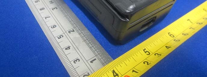
Click to zoom
Application Details
- Equipment Class
- TNF - Licensed Non-Broadcast Transmitter Held to Face
- Date of Grant
- Jul 30, 2014
- Application Purpose
- Original Equipment
- Date of Application
- Jul 30, 2014
- Equipment Note
- Two Way Radio
- Frequency Range
- 136.00000000 - 174.00000000
- Country
- China
Documents & Files
Document Text
Text extracted from the exhibit documents filed with the FCC. Open a document above to read the original.
Users Manual
DR6000-1 DR6100-1 DR7000-1 DR7100-1 Instruction Manual DMR/FM Portable Radio Thank you for purchasing a COVALUE two-way radio. This simple to use radio adopts the latest advances in technology, providing reliable communication in today’s demanding communication environment. Notice to the User: · Please read this instruction manual before operating this radio. · It’s prohibited to use the radio or charge it at any area with a potentially explosive atmosphere (where the air contains gas, dust and smog, etc.), as well as while taking on fuel, or while parking at a gasoline service station; or any area where radio communication is prohibited (such as a hospital or a airport.) · It’s prohibited to operate the radio without permission in areas where the government laws prohibit radio communication. · Please don't expose the radio to direct sunlight for a long time; don't place the radio near any heating devices, either. · Please don't put the radio in extremely dusty, moist humid areas or unstable surfaces. · Only qualified personal, with proper tools and instruments are allowed to service and repair the radios, do not disassemble the radio by yourself to avoid damages. FCC Warning: This devi ce complies with part 15 of the FCC Rules. Operation is subject to the following two conditions: (1) This device may not cause harmful interference, and (2) this device must accept any interference received, including interference that may cause undesired operation. Any Changes or modifications not expressly approved by the party responsible for compliance could void the user’s authority to operate the equipment. IC Warning : This dev ice complies with Industry Canada licence-exempt RSS standard(s). Operation is subject to the following two conditions: (1) this device ma y not cause interference, and (2) this device must accept any interference,including interference that may cause undesired operation of the device. Under Industry Canada regulations, this radio transmitter may only operate using an antenna of a type and maximum (or lesser) gain approved for the transmitter by Industry Canada. To reduce potential radio interference to other users, the antenna type and its gain should be so chosen that , the equivalent isotropically radiated power (e.i.r.p.) is not more than that necessary for successful communication. This equipment can be used in member states of the European Union once the corresponding administrative licence is obtained. DECLARATION OF CONFORMITY SHENZHEN COVA LUE COMMUNICATIONS CO.,LTD. as manufacturer of the product two way radio, declares that the said product complies with the essential requirements established in article 3 of the Council of Europe Directive 1999/5/CE, dated 9th March, 1999.1999. SHENZ H EN COVALUE COMMUNICATIONS CO., LTD. Le présent appareil est conforme aux CNR d'Industrie Canada applicables aux appareils radio exempts de licence. L'exploitation est autorisée aux deux conditions suivantes: (1) l'appareil ne doit pas produire de brouillage, et (2) l'utilisateur de l'appareil doit accepter d'en compromettre le fonctionnement. même si le brouillage est susceptible tout brouillage radioélectrique subi, Under Industry Canada regulations, this radio transmitter may only operate using an antenna of a type and maximum (or lesser) gain approved for the transmitter by Industry Canada. To reduce potential radio interference to other users, the antenna type and its gain should be so chosen that, the equivalent isotropically radiated power (e.i.r.p.) is not more than that necessary for successful communication. Conformément à la réglementation d'Industrie Canada, le présent émetteur radio peut fonctionner avec une antenne d'un type et d'un gain maximal (ou inférieur) approuvé pour l'émetteur par Industrie Canada. Dans le but de réduire les risques de brouillage radioélectrique à l'intention des autres utilisateurs, il faut choisir le type d'antenne et son gain de sorte que la puissance isotrope rayonnée équivalente (p.i.r.e.) ne dépasse pas l'intensité nécessaire à l'établissement d'une communication satisfaisante. Le présent appareil est conforme aux CNR d'Industrie Canada applicables aux appareils radio exempts de licence. L'exploitation est autorisée aux deux conditions suivantes: (1) l'appareil ne doit pas produire de brouillage, et (2) l'utilisateur de l'appareil doit accepter d'en compromettre le fonctionnement. même si le brouillage est susceptible tout brouillage radioélectrique subi, Under Industry Canada regulations, this radio transmitter may only operate using an antenna of a type and maximum (or lesser) gain approved for the transmitter by Industry Canada. To reduce potential radio interference to other users, the antenna type and its gain should be so chosen that, the equivalent isotropically radiated power (e.i.r.p.) is not more than that necessary for successful communication. Conformément à la réglementation d'Industrie Canada, le présent émetteur radio peut fonctionner avec une antenne d'un type et d'un gain maximal (ou inférieur) approuvé pour l'émetteur par Industrie Canada. Dans le but de réduire les risques de brouillage radioélectrique à l'intention des autres utilisateurs, il faut choisir le type d'antenne et son gain de sorte que la puissance isotrope rayonnée équivalente (p.i.r.e.) ne dépasse pas l'intensité nécessaire à l'établissement d'une communication satisfaisante. ed for general population, consumer, or any FCC/IC limits. This radio device is NOT authoriz INSTRUCTIONS TO ENSURE COMPLIANCE WITH THE FCC/IC’S RF EXPOSURE AND OPER ATIONAL INSTRUCTIONS FOR THE OCCUPATIONAL USE RF ENERGY EXPOSURE AWARENESS AND CONTROL INFORMATION, REQUIREMENTS BEFORE USING YOU R PORTABLE 2-WAY RADIO, READ THIS IMPORTANT RF ENERGY AWARENESS AND CONTROL INFORMATION AND OPERATIONAL GUIDELINES NOTICE: This radio is intended for use in occupational/controlled conditions, where users have full knowledge of their exposure and can exercise control over their exposure to meet…
Text truncated - open the document above for the full version.
Block Diagram
1 2 3 4 5 6 78 ABCD 8 7 6 5 4 3 2 1 D CBA ANT LPF Q107RD07 D101 HVU131 RF AMP ANT SW Q105 2SK3475 RF AMP IC619 UPB1509BV 1/2 Q1012SC5066 RF AMP D100,D109MA2S077 T/RSW Q100 2SC5066 RF AMP Q6 2SC5066 BUFFAMP Q22SC5066 RF AMP Q4 2SK508 TX VCO Q7,Q5 2SJ243,UMC4 DC SW Q3 2SK508 RX VCO Q8 2SC4617 RIPPL FILTER LoopFilter 16.8MHz IC607SKY72310 5C T/R PLL_3V3 DET Q108 DTC144EE DCSW APCSW CURRENT IC100 NJM2904V B APC PLL_DATPLL_CLKPLL_CS Q2033SK318 D204 RF AMP BFP D203D905 BFP Q202 3SK318 1st MIXER XF201 49.95MHz First IF Q201 2SC5066 IF AMP CF200 450MHz IF Q1 2SC5066 X3 CD200 450KHz 5R IC603XC6204B502MR Q604DTA123JE IC604XC6204B502MR 5T 5RC IC618XC6204B332MR IC605MP2359DJ 3V3 Q3072SK1588 Q401 DTC114EE MUTE DC SW SW IC302TDA2822D AF D401 GREEN AMP LED Q306DTC144EE DCSW Q304DTC144EEDCSW Q305 2SA1362 DCSW PROTECT Q400 DTC114EE DC SW D400 RED LED IC613 FLASH X603 8MHz + - D202 APC Second EN0EN3GND BATT PWR SW / VOL SP MIC EXT SW SB SB AFCO CH SW IC200NJM2591V RSSIBUSY 5R 5R 5R 5C 5C 5T 5C APC PTTSW1SW2ALARM BAT+ BAT+ TX_LED RX_LED IC614 MICROPROCESSOR XOUT XIN 3V3 RESETVOXBUSYRSSI EN0EN1PTTSW1 SW2 5TC5RCAFCOAPCSWAPCPLL_DATPLL_CLKPLL_CS ... ... IC500BNJM2900V AMP IC500ANJM2900V AMP 5M 5M VOX POW_SW IC300B IC300A DCS-IN LPF AMP IC300C HPF IC300D HPF NJM2902V 5C_A 5C_A 5C_A 5C_A IC301B LPF IC301ANJM2904V LPF 5C_A 5C_A 136-174MHz DR6000-1 DR6100-1 DR7000-1 DR7100-1 BLOCK DIAGRAM VER 1.0 TitleSize A3 Number Revision Date:File: Sheet ofDrawn By: X602 29.4912MHz IC806 PROCESSOR XIN 3V3 DMR_SCLKDMR_SDIDMR_SDOI2S_FS ... ... DMR_CS MOD1 Q308 SW ... ... SW 5TC 5M5R LAMPLCD... LCD MODULE K1~8 4X4 KEY BOARD 5R CU7000-1CU7100-1 CU7000-1CU7100-1 BAIS BAND IC601 TC75S51F AF AMP Q608 AMP PBR951 DMR_VCC IF_OUT IC608A AMP NJM2904V IC608B AMP MOD2 CTC/DCS_OUT EN1EN2 FM_MUTE 5R BAT+ Q606FMMT717 POW_SW BAT+ POW_C POW_DET IC602XC6204B502MR Q610UMC4A FM_SW 5C 5C_A
Cover Letter(s)
DR6000-1, DR6100-1, DR7000-1, DR7100-1 are just different in model name. that are declared similar are as follows: A description of the differ me: DR7000-1. SHENZHEN COVALUE COMMUNICATIONS CO., LTD. Add: 2/F., Bldg. 24, XiLi Industrial Park, No.119 Xinguang Rd, Xili, Nanshan, Shenzhen, China Tel: 0755‐86345789 Fax: 0755‐86345790 DECLARATION OF SIMILARITY Date : 2014-02-07 To: Bay Area Compliance Laboratories Corp. (Dongguan) No.69 Pulong Village Puxinhu Industry Zone Tangxia, Dongguan, China http://www.baclcorp.com Dear Sir or Madam: We, SHENZHEN COVALUE COMMUNICATIONS CO., LTD., hereby declare that product: Two way radio, model: DR6000-1, DR6100-1, DR7100-1 is electrically identical with the same electromagnetic emissions and electromagnetic compatibility characteristics as model na ences between the tested model and those Please contact me should there be need for any additional clarification or information. Best Regards, Shu, Chengtao Research & Development Department Manager
External Photos
EXHIBIT B - EUT EXTERNAL PHOTOGRAPHS EUT – All View EUT – Top View EUT – Bottom View EUT – Side View EUT –Side View EUT – Antenna View EUT – Base Top View EUT – Base Bottom View EUT – Adapter View EUT – Adapter Label View
ID Label/Location Info
EXHIBIT A - FCC ID LABELING AND LOCATION FCC ID Label FCC ID Label Location The label shown shall be permanently affixed at a conspicuous location on the device and be readily visible to the user at the time purchase (Labeling requirements per 2.925)
Internal Photos
EXHIBIT C - EUT INTERNAL PHOTOGRAPHS EUT – Uncover View EUT – Battery View EUT – Uncover View EUT –Cover Off View EUT – Board View EUT – Main Board Top View EUT – Main Board Bottom View EUT – Sub-board Top View EUT – Sub-board Bottom View
Operational Description
136 to 174MHz,The frequency c 1 Circuit Description 1 Frequency configuration The reference frequency of frequency synthesizer is provided by 16.8MHz crystal oscillator X1 TCXO. The receiver adopts quadric mixing mode. The first IF is 49.95MHz, and the second IF is 450kHz. The first local oscillation signal of the receiver is produced by frequency synthesizer and the second local oscillation signal selects the 4 rd harmonics of 16.8MHz of crystal oscillator X1 TCXO. The signal of transmitter is produced by frequency synthesizer directly. Figure 1 Frequency configuration 2 Receiver(Rx) The receiver is double conversion superheterodyne,designed to operate in the frequency range of onfiguration in Fig 1.1 Figure 2 Receiver section configuration Front End of Receiver Signals from the antenna are filtered by BPF via RX/TX switch (D101 D102 and D103). After being filtered out the useless out-of-band signals, the signals are amplified by LNA consisting of Q203 and external components. Signals from LNA are filtered again by BPF before entering the 1st mixer (Q202). 2 The PWM wave is output by MCU composed of 58 foot and then commutated to adjustable voltage after filtering to change the capacity of varactor diode D905 D203 D202 and D204 to control the center frequency of BPF. 1 st mixer The first IF (49.95MHz) signal is produced after mixing of the receiving signal from LNA and the 1 st local oscillation signal from frequency synthesizer. The first IF signal is filtered out adjacent channel and other useless signals by crystal filter (XF201). IF Circuit The 1 st IF signal from crystal filter is amplified by the first IF amplifier (Q201) before processing of IC in IF( IC200,NJM2591V). IF IC consists of the 2 nd mixer, 2 nd local oscillation, IF amplifier, limiter, frequency discriminator and noise amplifier. Frequency (16.8MHz) produced by TCXO(X1) is amplified and then selects 3 rd harmonics (51.4MHZ) as the second local oscillator signal source. The second IF signals (450kHz) are generated after signals mixing of the second local oscillation (51.4MHz) and the first IF (49.95MHz) in IC200. Audio signals are demodulated and outputted by IC200 after the second IF signals are amplified and limited in IC200 and then filtered by ceramic filter(450kHz). Figure 3 Schematic Diagram for IF System Receiving Audio Signal Processing: 3 The audio processing circuit of receiver consists of IC300. Voice signals from IC300 are sent to IC301 (CTCSS signaling filter circuit. Squelch Circuit Part of the AF signal from the IC200 enters the FM IC again,and the noise component is amplified and rectified by a filter and an amplifier to produce a DC voltage corresponding to the noise level. The DC signal from the FM IC goes to the analog port of the microprocessor(IC403).IC403 determines whether to output sounds from the speaker by checking whether the input voltage is higher or lower than the preset value. To output sounds from the speaker,IC403 sends a high signal to the MUTE and AFCO lines and turns IC302 on through Q302 Q304 and Q305. Audio Power Amplification The audio power amplifying circuit consists of IC302 and the peripheral components. The signals are amplified by audio power amplifier to drive the speaker after collecting the receiving audio signals, voice signals and warning tone signals. The warning tone has no volume limitation. When AFCO is high level, Q304 is on, IC302 begins to work and the speaker sounds. Speaker Impedance: 16ohm CTCSS Signal filtering The audio signals after demodulation in IC200 may contain CTCSS (continuous tone control squelch system) or DCS(digital squelch)signals. The spectrum component of CTCSS/DCS is 67 to 250Hz. The filtering circuit composed of IC301 can filter out signals except CTCSS/DCS spectrum, which makes MCU decode the CTCSS/DCS more accurately. 3 Transmitter (Tx) Transmitter Power Amplifier Figure 4 Schematic Diagram for Power Amplifier and Antenna Switch The modulated RF signals from VCO are amplified by Q101 and Q105 before the power amplification in Q107. Gate bias of Q105 and Q107 is controlled by APC circuit, so the output power of transmitter can be controlled conveniently by changing the gate bias voltage. 4 APC(Automatic Power Control) Figure 5 Schematic Diagram for APC Circuit R130 R131 and R132 are power amplification current detector, IC100A is power amplification current sampling amplifier and IC00B is power comparison amplifier. The power amplification current and IC100A output will increase with oversized output power of transmitter. When the output voltage of IC100B decreases, the bias voltage of Q105 and Q107 will decrease, finally the output power of transmitter will decrease or vice versa. Thus, the output power of transmitter will keep stable under any different working condition. MCU can set the power by changing the voltage input to IC100B. Audio Signal Processing of Transmitter Figure 6 Schematic Diagram for Audit Circuit of Receiver The audio signal processing circuit of Transmitter consists of IC601 and IC609. Voice signals from MIC are sent to VCO for modulation together with CTCSS/DCS after amplification, limitation and filtering. IC609 is a bais band processor. AGC circuit consists of D601, D602 and Q602,Q603. The signal amplitude is reduced to ensure no distortion in case of oversized MIC signal. Q601, the power switch of voice processing circuit, controlled by MCU, will give power supply to IC601 only during transmission. J501 is the socket for external MIC, and the internal MIC will disconnect automatically when using 5 external MIC, but the internal PTT is still effective. 4 PLL Frequency Synthesizer Figure 7 Schematic Diagram for Frequency Synthesizer The DR6000-2 adopts PLL frequency synthesizer. Frequency synthesizer consists of reference oscillator, voltage controlled oscillator (VCO), programmable frequency divider (PFD), phase comparator and low pass filter (LPF). RX VCO Unit consists of Q3 D1 D3 L13 C34 C38 C39 and C42. TX VCO U…
Text truncated - open the document above for the full version.
Parts List/Tune Up Info
1 ADJUSTMENT 1 Required Test Equipment Table 1 Number Name Parameter requirements 1 Computer Above P2, compatible IBM PC, WINDOWS 98/ME/2000/XPOperating System 2 Programming software ARD001 3 Programming cable 4 Dubbing cable CPL-01 5 DC regulator Output voltage:7.4V, output electric current:≥ 5A 6 RF power meter Test range: 0.5---10W Frequency range: 100MHz—500MHz Resistance: 50Ω SWR≤1.2 7 Frequency meter Frequency range: 0.1—600MHz Frequency accuracy: higher than±1×10 -6 Sensitivity: higher than 100mV 8 Frequency deviator Frequency range: DC—600MHz Test range: 0--±5kHz 9 DMM Input resistance: above 10MΩ/V DC, capable of measuring voltage, electric current and resistance. 10 Audio signal generator Frequency range:2---3000Hz Output level: 1---500mV 11 RF po wer attenuator Decrement: 40db or 50db Receive power : higher than10W 12 Standard signal source Frequency range:10MHz---1000MHz Output level:0.1uV~32mV (-127dBm~-17dBm) 13 Oscillograph Frequency range: DC~20MHz Test range: 10mV~20V 14 Audio Frequency voltmeter Test range: 10mV~10V Recommend how to use: item 6, 7, 8, 10, 11 and 12 which listed in the table can be substituted by integrated tester HP8920/HP8921. 2 Figure 1 External Speaker/microphone Interface Definition 2 Adjustment Items Some detection and adjustment shall be made to the station technical data after changing the components during the maintenance. The debugging introduction of some related circuits goes as follows: Some parameters of the product can be adjusted (“Interphone Performance Tuning”) by use of ARD001 Programming Software of our company. The adjustable parameters are as follows: 1) Frequency stability” 2) Transmitting power 3) Alarm threshold for battery low-voltage 4) Squelch level 5) QT frequency offset 6) DCS frequency offset 7) Receiving sensitivity Steps for adjustment: a、Enter Computer Test Mode by selecting “Test Mode” in main menu of ARD001 Programming Software. b、Select the items to be adjusted in choice menus, and then adjust the parameters by function keys on the computer keyboard. c、Exit Computer Test Mode after adjustment. 3 Adjustment 3.1 VCO Adjustment Close “Power-saving Mode”. Set receiving frequency to low frequency point (see Table 2) and in the receiving state, test voltage of PD by DMM and adjust fine-tuning capacitor TC1/TC2 to get CV voltage of 1.0V±0.2V Set transmitting frequency to high frequency point (refer to Table 2), press PTT and test voltage of PD by DMM, which shall less than 4.0V 3 Table 2 High/ Intermediate/ Low Frequency Point of All Models Low Frequency Point Intermediate Frequency Point High Frequency Point DR6000-1 DR6100-1 DR7000-1 DR7100-1 136.000 MHz 155.100 MHz 173.975 MHz 3.2 PLL frequency calibration Double-click to enter “Frequency Stability” in “Interphone Performance Tuning” to achieve the rated transmitting frequency by adjusting the number from 0 to 255 (Error<200Hz). 3.3 Transmitting frequency adjustment Double-click to enter “Transmitting High Power” in “Interphone Performance Tuning” to adjust the five frequency points including ”Lowest”, “Low”, “Mid”, “High” and “Highest” respectively and set transmitting power to over 4W by adjusting the number from 0 to 255 and observe the operating current (≤1.6A) at the same time. Double-click to enter “Transmitting Low Power” in “Interphone Performance Tuning” to adjust the five frequency points including ”Lowest”, “Low”, “Mid”, “High” and “Highest” respectively and set transmitting power to over 1W by adjusting the number from 0 to 255. 3.4 Transmitting low-voltage alarm Adjust power voltage to 5.8V and double-click to enter “Transmitting Low Voltage” in “Interphone Performance Tuning” Mode for automatic detection of the software, and then click “Save” for exit after no or little variation in numbers. 3.5 Frequency offset adjustment Input audio signal (12mV, 1000Hz) at MIC jack of interphone. Adjust the potentiometer VR501 and set frequency offset to ±4.2kHz. 3.6 DCS transmitting signal waveform and frequency offset adjustment Double-click to enter “DCS frequency offset” in “Interphone Performance Tuning” Mode, adjust potentiometer VR1 to observe demodulated signal (the waveform shall be smooth and similar to square wave), and then click “Broadband” to adjust all points including ”Lowest”, “Low”, “Mid”, “High” and “Highest” respectively for frequency offset of 0.8kHz. After that, click “Narrowband” to adjust the frequency offset to 0.4kHz. 3.7 CTCSS frequency offset adjustment Double-click to enter “QT(67) frequency offset” in “Interphone Performance Tuning” Mode and click “Broadband” to adjust the five frequency points including ”Lowest”, “Low”, “Mid”, “High” and “Highest” respectively to 0.75kHz and then click “Narrowband” to adjust the frequency offset to 0.35kHz. Select “QT(254) frequency offset” in “Interphone Performance Tuning” Mode, and the debugging method 4 is the same as that of “QT(670) frequency offset”. 3.8 Receiving Sensitivity Double-click to enter “Receiving Sensitivity” in “Interphone Performance Tuning” Mode to adjust the five frequency points including ”Lowest”, “Low”, “Mid”, “High” and “Highest” respectively and the number from 0 to 255 for setting max sensitivity of all points. 3.9 Receiver Squelch setting Double-click to enter “SQL9 open” in “Interphone Performance Tuning” Mode and click “Broadband” to make the frequency of the transmitting signal corresponding to the receiving frequency (level of -116dBm, modulation signal of 1kHz and frequency offset of 3kHz) showed at each frequency point of the software. Enter all points including ”Lowest”, “Low”, “Mid”, “High” and “Highest” respectively for automatic adjustment of software and then press next point after no big change to numbers. After that, adjust “Narrowband”, the debugging method is the same as that of “Broadband” except the input modulation signal is changed to frequency of 1kHz and frequency offset of 1.5kHz. Select “SQL9 open” in “Interphone Performance Tuning” Mode and click “Broadba…
Text truncated - open the document above for the full version.
RF Exposure Info
Note: This test report is prepared for the customer shown above and for the device described herein. It may not be duplicated or used in part without prior written consent from Bay Area Compliance Laboratories Corp. SAR EVALUATION REPORT For SHENZHEN COVALUE COMMUNICATIONS CO., LTD. 2/F, Bldg. 24, XiLi Industrial Park, No.119 Xinguang Road, Xili, Nanshan, Shenzhen, Guangdong, China FCC ID: Y4GDR6000-1 Report Type: Original Report Product Type: VHF Two Way Radio Test Engineer: Wilson Chen Report Number: R1DG140126005-20A Report Date: 2014-08-11 Reviewed By: Bell Hu SAR Engineer Prepared By: Bay Area Compliance Laboratories Corp. (Shenzhen) 6/F, the 3rd Phase of WanLi Industrial Building, ShiHua Road, FuTian Free Trade Zone Shenzhen, Guangdong, China Tel: +86-755-33320018 Fax: +86-755-33320008 www.baclcorp.com.cn Bay Area Compliance Laboratories Corp. (Shenzhen) Report No: R1DG140126005-20A SAR Evaluation Report 2 of 64 Attestation of Test Results EUT Information Company Name Shenzhen Covalue Communications Co., Ltd. EUT Description Two Way Radio FCC ID Y4GDR6000-1 Model Number DR6000-1, DR6100-1, DR7000-1, DR7100-1 Test Date 2014-07-15 Mode Frequency (MHz) Max. SAR Level(s) Reported (1g) Limit (W/Kg) Digital 136-174 12.5 kHz Face up: 0.216 W/kg Body-Back: 1.315 W/kg 8 Analog 136-174 12.5 kHz Face up: 0.161 W/kg (50% duty cycle) Body-Back: 1.519 W/kg (50% duty cycle) Applicable Standards ANSI/IEEE C95.1: 2005 IEEE Standard for Safety Levels with Respect to Human Exposure to Radio Frequency Electromagnetic Fileds,3 kHz to 300 GHz. ANSI/IEEE C95.3: 2002 IEEE Recommended Practice for Measurements and Computations of Radio Frequency Electromagnetic Fields With Respect to Human Exposure to SuchFields,100 kHz—300 GHz. IEEE1528: 2013 IEEE Recommended Practice for Determining the Peak Spatial-Average Specific Absorption Rate (SAR) in the Human Head from Wireless Communications Devices: Measurement Techni ques KDB Procedures KDB 447498 D01 Mobile and Portable Devices RF Exposure Procedures and Equipment Authorization Policies. KDB 865664 D01 SAR measurement 100 MHz to 6 GHz v01. KDB 643646 SAR test Reduction Considerations for Occupational PTT Radios. KDB Inquiry: Tracking Number 316436 for SAR VHF system validation. Note: This wireless device has been shown to be capable of compliance for localized specific absorption rate (SAR) for Occupational /Controlled Exposure limits specified in ANSI/IEEE Standards and has been tested in accordance with the measurement procedures specified in IEEE 1528-2003 and RF exposure KDB procedures. The results and statements contained in this report pertain only to the device(s) evaluated. Bay Area Compliance Laboratories Corp. (Shenzhen) Report No: R1DG140126005-20A SAR Evaluation Report 3 of 64 TABLE OF CONTENTS DOCUMENT REVISION HISTORY ............................................................................................................................ 5 EUT DESCRIPTION ........................................................................................................................................................ 6 TECHNICAL SPECIFICATION............................................................................................................................................. 6 REFERENCE, STANDARDS, AND GUILDELINES ................................................................................................. 7 SAR LIMITS ..................................................................................................................................................................... 8 FACILITIES ...................................................................................................................................................................... 9 DESCRIPTION OF TEST SYSTEM ........................................................................................................................... 10 EQUIPMENT LIST AND CALIBRATION ................................................................................................................ 17 EQUIPMENTS LIST & CALIBRATION INFORMATION ...................................................................................................... 17 SAR MEASUREMENT SYSTEM VERIFICATION ................................................................................................ 18 LIQUID VERIFICATION ................................................................................................................................................... 18 SYSTEM ACCURACY VERIFICATION .............................................................................................................................. 20 SAR SYSTEM VALIDATION DATA ........................................................................................................................ 21 EUT TEST STRATEGY AND METHODOLOGY .................................................................................................... 25 TEST POSITIONS FOR DEVICE OPERATING NEXT TO A PERSON’S EAR ......................................................................... 25 CHEEK/TOUCH POSITION .............................................................................................................................................. 26 EAR/TILT POSITION ....................................................................................................................................................... 26 TEST POSITIONS FOR BODY-WORN AND OTHER CONFIGURATIONS ................................................................................ 27 SAR EVALUATION PROCEDURE .................................................................................................................................... 28 TEST METHODOLOGY .................................................................................................................................................... 28 CONDUCTED OUTPUT POWER MEASUREMENT ............................................…
Text truncated - open the document above for the full version.
Schematics
1 2 3 4 5 6 7 8 9 10 11 12 13 ABCDE 13 12 11 10 9 8 7 6 5 4 3 2 1 E DCBA C25470p L627n C292p Q400 DTC114EE Q401DTC114EE R402220R R40322R C406470p R426 8.2k C402470p R4108.2k D400 RED D401 GREEN R41710R R50R C120.1u R70R R100R R956R C152.2u C180.1u R130R R1510k R40R C1047p R8330k Q1 2SC5066 L4330n C17270p C190.01u L16220n C1647p L17 220n L5560n C26330p C5122p C28 22p C200.01u R14100R L7601s R20560R Q2 2SC5066 C543p R21100k R418 1k C3160.01u C3020.1u C312 0.01u C320 0.033u C3210.033u C3050.01u C3096800p R340120k R315 390k R31212k R314 470k R3033.3k R30091k R32122k R322220k SP R3110R R3041MR33847k R3015.6k R307 47k R3025.6k R306 220k R329 R3245.6k R3265.6k C3131u C3008200p C318 0.033u C319 0.047u C3085600p R316120kR31339k R30518k R323 100k R318 100k R325 100k R207 R205 3.9k R320120k C3112.2u C338 56p C20847p C3141000p C206220p C205 220p C202 100p C2140.01u C2070.1u C2110.039u C21233p C2100.1u R202100k R2011.8k R206750k R208680k R210220R R211220R R2092.7k Q2012SC5066 C2210.01u C223 10p C2090.1u C215 12p R327 10k Q307 ST2302 C3300.01u C335 0.1u C9310.47u R335 R33410R R332 4.7R Q306 DTC144EE Q304DTC144EE C3360.01u C3340.01u C9321000p R336 R333 470k R3311.5k R339 8.2k R145 180k R14133kR142470k R146 R137150k R138150k R135150k R133150k R1400R R136 150k C134 56p C132 C141 C139470p R134150k R1442.2k R1320.39R R1300.39R R1310.39R TH102 47k C165470p R1533.3k R152390R R50647k C5051u C5250.1u L500 601s R5341.8k R535470R C529 C531 F500 3.0A C528470p R53722R R53622R R341100k C3220.1u R3281k C2560.1u C30710u R20010R C200 10u Q110DTC114TE C203470p R2033.3k R2043.3k R308 10k R309 470k C3030.1u C204 4700p C2010.01u C213 C3060.01u C3010.018u C530 L501221s RF AMP AUDIO AMP ACTIVE FILTER AUDIO MUTE SW LED TX LED BUSY R4131k DR6000-1 DR6100-1 DR7000-1 DR7100-1 DR: 14.01.18 File: STAND: CHKD: Date Sheet 01 APPD: VER 1 CD200450KHz C30410u R317270k Q3002SC4617(S) R9011k C640.1u C630.1u R910 R912 R911 R914 R913 R917 R915 R909 R916 C9150.1u C912 C911 C909 C910 C908 R918 R922 R919 R921 R920 C914 C916 J501 2.5mm J500 3.5mm Q106 DTC144EE D903 Q902 DTA143ZE Q903DTC144EE C9240.01u R95822k L502221s C3310.1u C333 0.1u C533 220p C9390.01u 12 3 4 1234 R955 TH201 Q200 C9610.01u Q3052SA1362 C3270.1u R330 47k C962 0.01u C963 0.01u Q303 R9594.7R C965 D402 GREEN C969 1u R9660R R969470R OUT IN XF201 49.95MHz R97210k R9730R 17 8 14 VSS VDD + - + - + - + - IC300 NJM2902V 45 8 1IC100NJM2904V 45 8 1IC901 45 8 1IC301NJM2904V FILOQUAD FILI IFODEC…
Text truncated - open the document above for the full version.
Contact Information
Applicant
Chengtao Shu(Engineer)
Test Firm
Bay Area Compliance Laboratory Corp. (Shenzhen)John Chan
Technical Specifications
| # | Rule Parts | Frequency Range | Power Output | Emission | Tolerance |
|---|---|---|---|---|---|
| 3 | 9 | 136 MHz - 174 MHz | 5.27 W | 7K60FXW | 0.4 ppm |
Other Applications from SHENZHEN COVALUE COMMUNICATIONS CO., LTD.
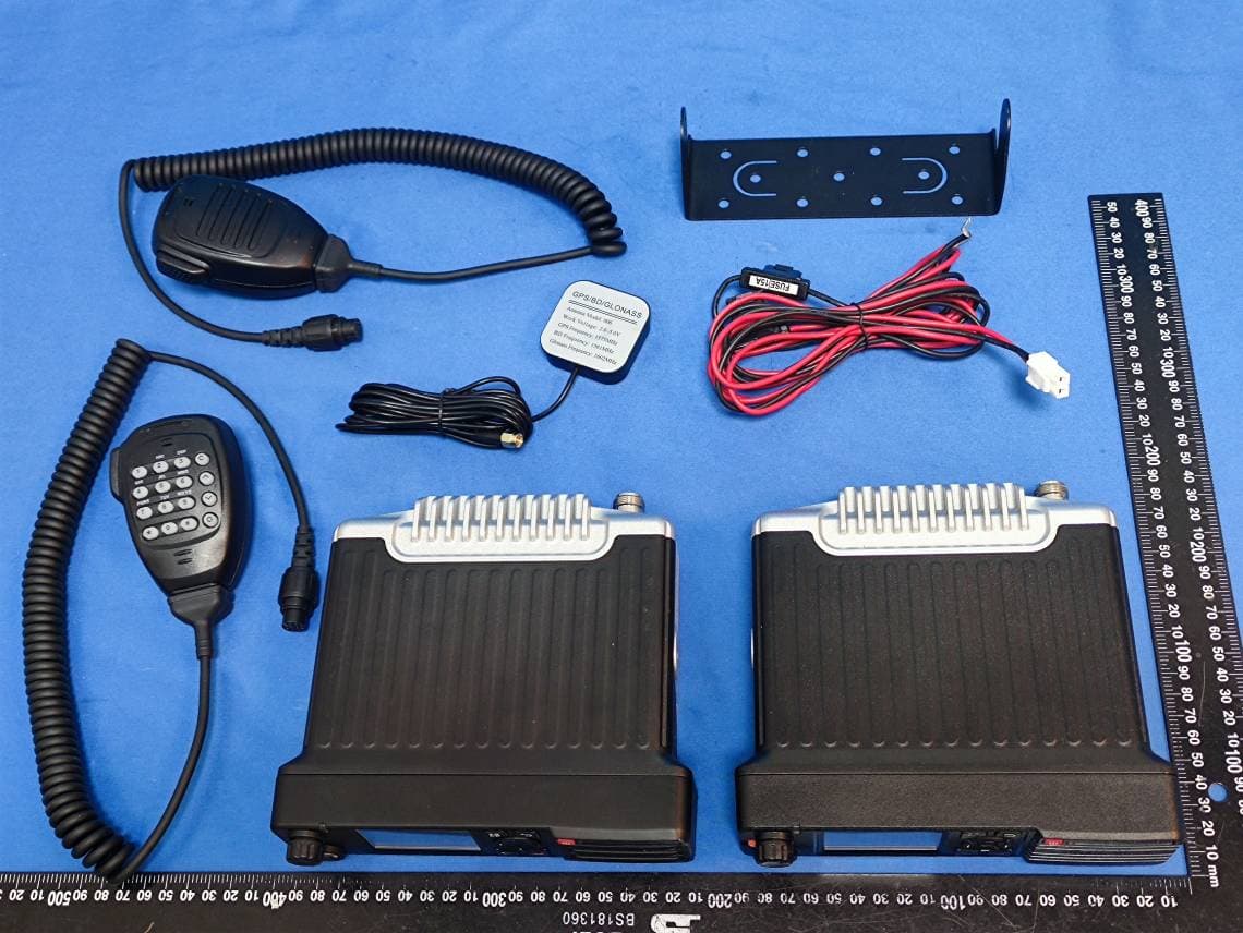
Y4GDM8000-2
Sep 11, 2024Mobile Radio
Equipment Class
DTS - Digital Transmission System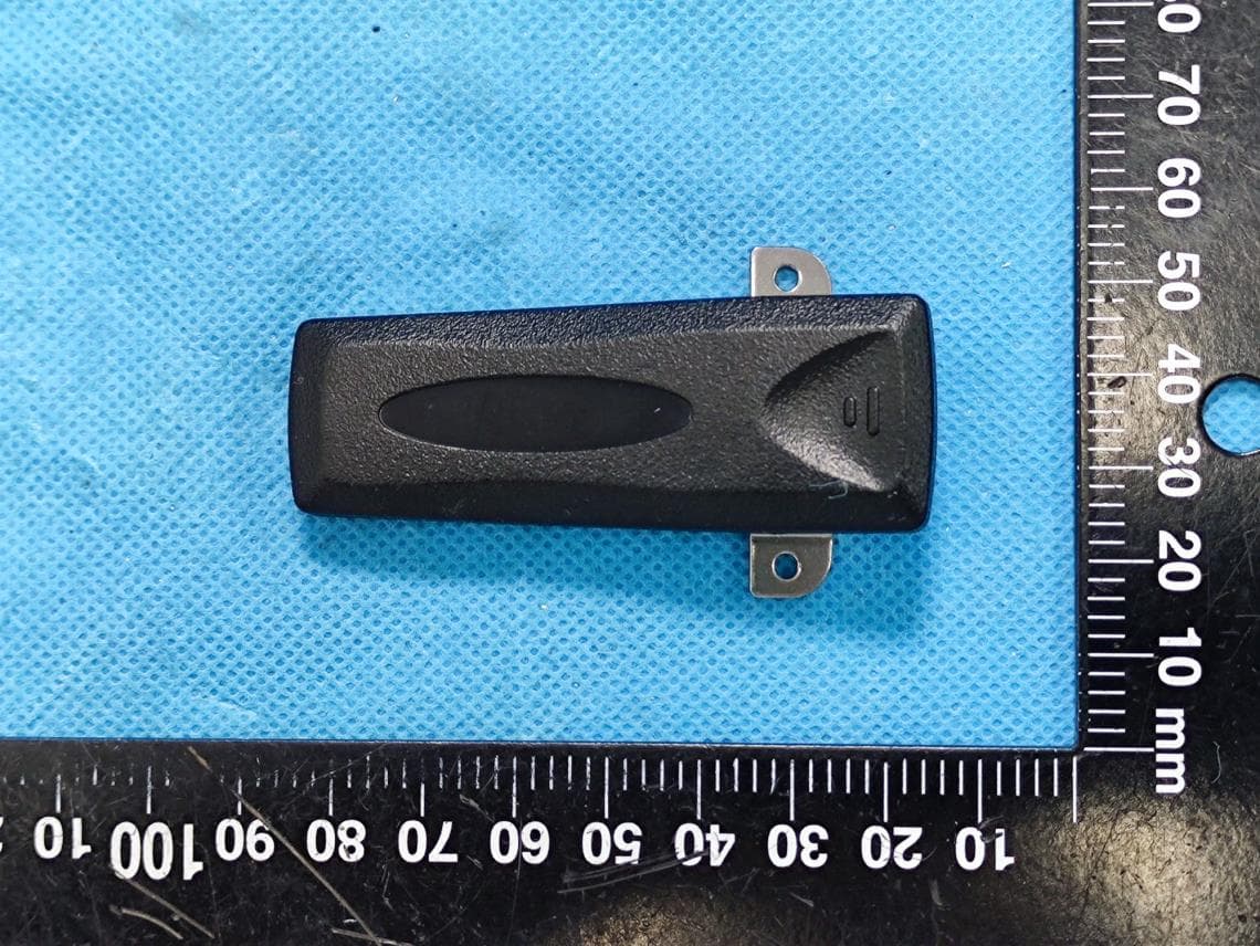
Y4GDR5810S-1
Jul 17, 2022Two Way Radio
Equipment Class
TNF - Licensed Non-Broadcast Transmitter Held to Face
Y4GDR5810-1
Mar 01, 2020Two Way Radio
Equipment Class
TNF - Licensed Non-Broadcast Transmitter Held to Face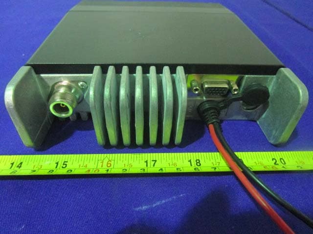
Y4GDM6000-1
Aug 20, 2015Mobile Radio
Equipment Class
TNB - Licensed Non-Broadcast Station Transmitter
Y4GDM6000-2
May 26, 2015Mobile Radio
Equipment Class
TNB - Licensed Non-Broadcast Station Transmitter