FCCID.CO- FCC ID Database
HomeCompaniesEquipment ClassesSearch

Β© 2026 FCC ID Database. All rights reserved.

AboutContactData sourced from FCC public records
  1. Home/
  2. DAZZLE MANUFACTURING LTD./
  3. YE6DAZZLE

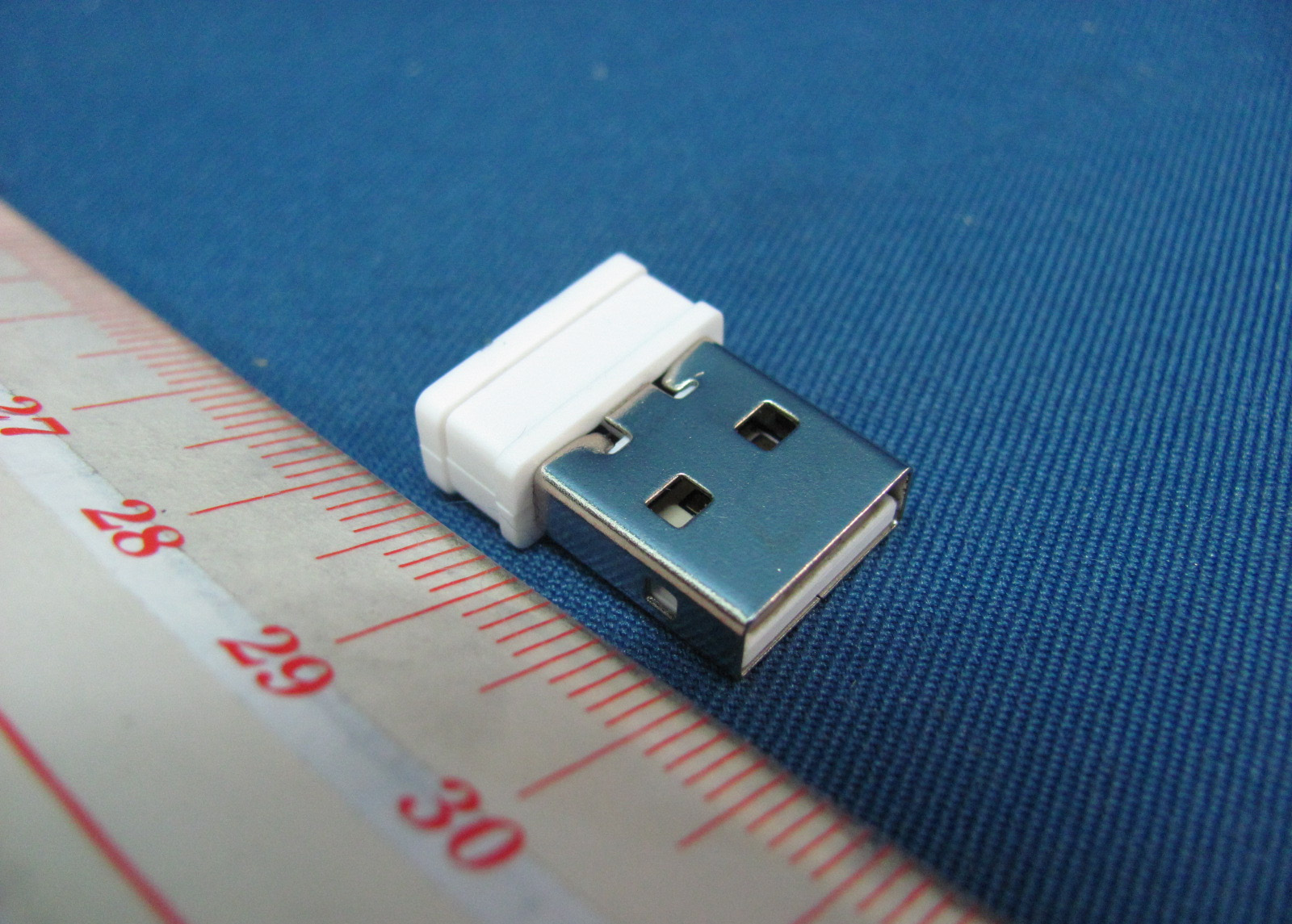
YE6DAZZLEWireless Mouse (Dongle)

DAZZLE MANUFACTURING LTD.
Wireless Mouse (Dongle) - FCC ID YE6DAZZLE - DAZZLE MANUFACTURING LTD.
Click to zoom

Application Details

Equipment Class
DXX - Part 15 Low Power Communication Device Transmitter
Date of Grant
Jun 14, 2011
Application Purpose
Original Equipment
Date of Application
Jun 14, 2011
Equipment Note
Wireless Mouse (Dongle)
Frequency Range
2402.00000000 - 2480.00000000
Company
DAZZLE MANUFACTURING LTD.
Country
Hong Kong

Documents & Files

Select a file to view

Users Manual

β†—
β†—

Block Diagram

β†—

Cover Letter(s)

β†—

External Photos

β†—

ID Label/Location Info

β†—

Internal Photos

β†—

Operational Description

β†—

Schematics

β†—

Test Report

β†—
β†—
β†—

Test Setup Photos

β†—
β†—

Document Text

Text extracted from the exhibit documents filed with the FCC. Open a document above to read the original.

Users Manual

DATE: 03.11.10 DIVISION: FA PRODUCT: Mouse Instructions NOTES: Artwork is scale. GRAPHIC SPECS PRINTED PAPER GRAPHICS ARE SCALE PRINTS CMYK FRONTBACK 8cm 10cm WIRELESS MOUSE INSTRUCTIONS WIRELESS MOUSE INSTRUCTIONS PANTONE 698 C PANTONE BLACK 7 U INSTALLATION: 1. Install 2 AAA batteries (not included). 2. Connect the USB reeiver to an open USB port on your computer or to a port on an additional USB hub. 3. Follow instructions that appear for driver installation. 4. Ensure that the USB receiver is connected. You may now start to use the mouse. PRODUCT FEATURES: Wireless optical mouse/USB receiver Product Specifications: 2.4 GHZ High Speed/10M Maximum distance Mini receiver/3 keys/Key lifecycle: 2,000,000/Resolution: 1000DPI SYSTEM COMPATIBILITY: Windows: 98/ME/2000/XP/Vista/MAC compatible CAUTION: Any changes or modifications not expressly approved by the party responsible for compliance could void the user’s authority to operate the equipment. Note: This equipment has been tested and found to comply with the limits for a Class B digital device, pursuant to part 15 of the FCC Rules. These limits are designed to provide reasonable protection against harmful interference in a residential installation. This equipment generates, uses and can radio frequency energy and, if not installed and used in accordance with the instructions, may cause harmful interference to radio communications. However, there is no guarantee that interference will not occur in a particular installation. If this equipment does cause harmful interference to radio or television reception, which can be determined by turning the equipment off and on, the user is encouraged to try to correct the interference by one or more of the following measures: β€’ Reorient or relocate the receiving antenna. β€’ Increase the separation between the equipment and receiver . β€’ Connect the equipment into an outlet on a circuit different from that to which the receiver is connected. This device complies with part 15 of the FCC Rules. Operation is subject to the following two conditions: (1) this device may cause harmful interference, and (2) this device must accept any interference recieved, including interference that may cause undesired operation. Features and speci!cations subject to change without notice. Microsoft, Windows and Windows Vista are either registered trademarks or trademarks of Microsoft Corporation in the United States and/or other countries. All trademarks and registered trademarks are the properties of their respective owners. All rights reserved. Β©2011 USB RECEIVER USB PORT

Block Diagram

Block Diagram of Dongle Unit FCC ID: YE6DAZZLE USB DATA  8PU83 (U2) 3V3 RF MU2400 (U1) 12MHz Crystal (Y1) PCB embedded antenna 2.402-2.480 GHz 3.3V Data SheetMU2400 MuChip Co., Ltd. Version 1.5.0 Confidential Page 9 of 55 July, 2009 18B_DDigital Output Battery detector output 19DVDD3Power Digital I/O power supply 20CEDigital Input Chip enable 21DMC_PAnalog Output Demodulator analog output, connecting to an external AC coupling capacitor 22DMC_NAnalog Input Demodulator analog input, connecting to an external AC coupling capacitor 23AVDD_IF Power RX IF power supply, voltage regulator output 24AVDD3 Power Voltage regulator power supply Back side plate GNDGround Table 1: Pin Function Description 3. Block Diagram DEMOD PLL On-Chip Switch RSSI IREFXC1XC2 IRQ CSn SCK MOSI MISO Voltage Regulator Filter FIFO IN/OUT CRC Code/ Decode ADDR Decode Data Slicer Clock Recovery Auto-ACK Protocol CE Mini MAC Figure 2: Block Diagram of RF Module RF I/O

External Photos

INTERTEK TESTING SERVICE Report No.: HK11050813-2 FCC ID: YE6DAZZLE Equipment Photographs Model : YTRUG281 (External)

Internal Photos

INTERTEK TESTING SERVICE Report No.: HK11050813-2 FCC ID: YE6DAZZLE Equipment Photographs Model: YTRUG281 (Internal) INTERTEK TESTING SERVICE Report No.: HK11050813-2 FCC ID: YE6DAZZLE Equipment Photographs Model: YTRUG281 (Internal)

Operational Description

FCC ID: YE6DAZZLE Model: YTRUG281 Technical Description of Dongle Unit The equipment under test (EUT) is the USB dongle unit (2.4GHz transceiver) of a wireless optical mouse system operating at 2.402GHz - 2.480GHz (79 channels, channel spacing 1MHz) using FSK technique . The Dongle side radio will always receives RF signal and checksum data at intervals. If data is valid it sends data via USB to computer, then send ACK data to Mouse Side Radio. Dongle side radio system is powered by PC USB port (5V). Modulation Type: FSK Antenna Type: Internal, Integral antenna The functions of main Components are mentioned as below. 1) U1 (MU2400) acts as 2.4GHz RF transceiver module. 2) U2 (8PU83) acts as USB controller dealing with internal data.. 3) Y1 generates 12MHz clock to RF transceiver Module (U1). MU2400 2.4GHz Low Data Rate RF Transceiver Data Sheet Version 1.5.0 July, 2009 MuChip Co., Ltd Data Sheet MU2400 MuChip Co., Ltd. Version 1.5.0 Confidential Page 2 of 55 July, 2009 MuChip RF Solution Provider --- World Wide Distributors For Any RF Application Design, Please Refer to www.muchip.com.tw Main Office: 3F, No.9, Park Avenue II, Science-Based Industrial Park Hsinchu, Taiwan, ROC Phone: +886-36668000 ext: 115 Email: [email protected] Data Sheet MU2400 MuChip Co., Ltd. Version 1.5.0 Confidential Page 3 of 55 July, 2009 MU2400 – 2.4GHz Low Data Rate RF Transceiver General Description The MU2400 is a single-chip FSK low data rate RF transceiver for the world wide 2.4 – 2.5GHz ISM band. The data rate of the MU2400 can be operated up to 1.6Mbps in buffer mode. The MU2400 uses the standard CMOS process to offer a complete FSK RF transceiver solution with small die size, low power consumption, minimum external parts and high reliability. The MU2400 consists of a fully integrated frequency synthesizer, a power amplifier, a crystal oscillator, a demodulator, modulator, and Auto-ACK protocol engine. A reduced off-chip filter is realized by the low-IF architecture in RX chain. The MU2400 is programmable for frequency channels, and protocol setup easily through a 4-wire SPI interface. Features z Single-chip FSK transceiver z Auto-ACK & Auto-retransmission z Star-Network with 6 channels z Address and CRC computation z 1/1.6Mbps data rate z 1 ~ 64 bytes payload length z 64 bytes FIFO size z 4-wire digital interface (SPI) z Power supply range: 1.8 to 3.6V z Battery low supply voltage detector z Support 4 power modes: Active/Standby/Idle/Power Down z Operation range: -40 o C to +85 o C z Standard CMOS process z 24-pin 4x4 QFN package z On-chip VCO, PLL and PLL loop filter z On chip channel filter Applications z Wireless mouse, keyboard, joystick z Keyless entry z Alarm and security system z Home automation z Surveillance z Automotive z Telemetry z Industrial sensors z Wireless data communication z Toys Data Sheet MU2400 MuChip Co., Ltd. Version 1.5.0 Confidential Page 7 of 55 July, 2009 1. Pin Configuration AVDD_IF DMC_N DMC_P DVDD3 AVDD3 CE 24 2322212019 18 17 16 15 14 13 7 89101112 1 2 3 4 5 6 QFN-24 4x4 MU2400 MuChip MISO MOSI SCK CSn EN_PA/IRQ_RSSI B_D IREF VREG_OUT AVDD_RF GND GND RFIO GND Exposed die attach pad XC1 XC2 DVDD IRQ (DR) VMOD A VDD_PLL Figure 1: Pin Configuration The exposed die attach pad must be connected to a solid ground plate because this is the main ground connection for the MU2400. Data Sheet MU2400 MuChip Co., Ltd. Version 1.5.0 Confidential Page 8 of 55 July, 2009 2. Pin Description Pin Name Type Description 1 IREF Analog Input Reference resistor pin, connect to an external resistor 2 VREG_OUT Power On-chip voltage regulator output 3 AVDD_RF Power RF power supply 4 GND Ground Connect to PCB ground 5 GND Ground Connect to PCB ground 6 RFIO Analog I/O RF input/output 7 VMOD Analog I/O Connect to external capacitor for filtering 8 AVDD_PLL Power PLL power supply 9 XC1 Analog I/O Be configured as the two pin definitions: a. Crystal pin1 for external crystal b. For external clock signal, it connects to ground. 10 XC2 Analog I/O Be configured as the two pin definitions: a. Crystal pin2 for external crystal b. For external clock signal, it’s the input pin of external clock 11 DVDD Power Digital power supply 12 IRQ(DR) Digital I/O Be configured as the two operation modes: a. IRQ: Interrupt signal in buffer mode b. DR: data input/data output in direct mode 13 MISO Digital Output Be configured as the two operation modes: a. master input/slave output in SPI mode b. data output in buffer mode 14 MOSI Digital Input Be configured as the two operation modes: a. master output/slave input in SPI mode b. data input in buffer mode 15 SCK Digital Input SPI input clock 16 CSn Digital Input SPI selection / programming enable 17 EN_PA/ IRQ_RSSI Digital Output Be configured as the two output modes: 1. EN_PA: To control the external PA chip 2. IRQ_RSSI outputs high – To indicate the MCU to read the RSSI digital registers, RSSI is only valid during receiving signal. – Let MCU know whether the channel is occupied. Data Sheet MU2400 MuChip Co., Ltd. Version 1.5.0 Confidential Page 9 of 55 July, 2009 18 B_D Digital Output Battery detector output 19 DVDD3 Power Digital I/O power supply 20 CE Digital Input Chip enable 21 DMC_P Analog Output Demodulator analog output, connecting to an external AC coupling capacitor 22 DMC_N Analog Input Demodulator analog input, connecting to an external AC coupling capacitor 23 AVDD_IF Power RX IF power supply, voltage regulator output 24 AVDD3 Power Voltage regulator power supply Back side plate GND Ground Table 1: Pin Function Description 3. Block Diagram DEMOD PLL On-Chip Switch RSSI IREFXC1XC2 IRQ CSn SCK MOSI MISO Voltage Regulator Filter FIFO IN/OUT CRC Code/ Decode ADDR Decode Data Slicer Clock Recovery Auto-ACK Protocol CE Mini MAC Figure 2: Block Diagram Data Sheet MU2400 MuChip Co., Ltd. Version 1.5.0 Confidential Page 17 of 55 July, 2009 10. Packet Handling Methods The packet handler offered by the MU2400 makes it possible to be operated up to the high data rate wi…

Text truncated - open the document above for the full version.

Schematics

55 44 33 22 11 D D C C B B A A RF_CE DPDN RF_MOSI VDD RF_IRQRF_SCKRF_CSnRF_MOSO DP DN VDDV33V33 RF_CE RF_CSnRF_SCKRF_MOSIRF_MOSORF_IRQ V33 V33 TitleSize Document Number Rev Date: Sheet of <Doc> <RevCode> USB-AT+MU-VER1.1 A 11 Tuesday, September 21, 2010 TitleSize Document Number Rev Date: Sheet of <Doc> <RevCode> USB-AT+MU-VER1.1 A 11 Tuesday, September 21, 2010 TitleSize Document Number Rev Date: Sheet of <Doc> <RevCode> USB-AT+MU-VER1.1 A 11 Tuesday, September 21, 2010 R162KR162K 1 TP4TP4 1 TP1TP1 R2 1M R2 1M C12105C12105 L4 4.7NH L4 4.7NH C7105C7105 C2 105C2 105 C11 33PC11 33P C8 104C8 104 C14 4pFC14 4pF R3 10E R3 10E C41nFC41nF C10 33PC10 33P C13 225C13 225 1 TP2TP2 PA0 1 PA1 2 PA2 3 PA3 4 PB4 5 PB6 6 VSS 7 VSS 8 VREG 9 VPP 10 XOUT 11 OVDD 12 VCC 13 DN 14 DP 15 PB2 16 PB1 17 PA7 18 PA6 19 PA5 20 PA4 21 U2U2 C16 1UFC16 1UF C6 1pFC6 1pF 1234 CN1USB2.0CN1USB2.0 C5 10UC5 10U L25.6NHL25.6NH 1 TP3TP3 C1 333C1 333 1 2 Y116MHzY116MHz C3 7pFC3 7pF VREG_OUT 3 SCAN-MODE 6 GND 7 RFIO 8 VMOD 10 AVDD_PLL 11 XC1 13 XC2 14 CSn 20 SCK 19 MOSI 18 MISO 17 IRQ/DR 16 DVDD 15 IREF 1 CE 25 DVDD3 24 B_D 22 EN_PA/IRQ_RSSI 21 AVDD_RF 5 DMC_P 26 DMC_N 27 AVDD_IF 28 AVDD3 30 GND 9 GND 12 GND 23 GND 29 GND 2 GND 31 U1 MU2400 U1 MU2400 2.402GHz - 2.480GHz FCC ID: YE6DAZZLE 12MHz

Test Report

INTERTEK TESTING SERVICES Report No. : HK11050813-2 Sample No. : 1/1 Code: FCC15C_e / Effective Date: 20 Dec 2010 ( of ) Bandedge Plot – Pursuant to FCC Part 15 Section 15. 249 Requirement (Pass ) marker1(peak) = 85.0dBuV/m marker1(peak) – delta = 85.0dBuV/m – 31.83dB = 53.17dBuV/m lower than 54dBuV/m limit marker1(peak) = 84.3dBuV/m marker1(peak) – delta = 84.3dBuV/m – 37.00dB = 47.30dBuV/m lower than 54dBuV/m limit

Test Report

Report no.: HK11050813-2 Mode: Transmitting 6DB AC 150 kHz30 MHz dBΞΌV dBΞΌV 1 PK CLRWR 2 AV CLRWR SGL TDS RBW 9 kHz MT 1 s PREAMP OFFAtt 10 dB AUTO 1 MHz10 MHz 0 10 20 30 40 50 60 70 80 90 100 CF15MAV CF15MQP HK11050813-1(E0813C1) Date: 10.JUN.2011 16:19:10 Report no.: HK11050813-2 Mode: Transmitting EDIT PEAK LIST (Final Measurement Results) Trace1: CF15MQP Trace2: CF15MAV Trace3: --- TRACE FREQUENCY LEVEL dBΞΌV DELTA LIMIT dB 1 Quasi Peak 150 kHz 44.31 N -21.68 1 Quasi Peak 226.5 kHz 36.67 L1 -25.90 HK11050813-1(E0813C1) Date: 10.JUN.2011 16:18:50

Test Report

- The test report only allows to be revised within the retention period unless further standard or the requirement was noticed. - This report is for the exclusive use of Intertek's Client and is provided pursuant to the agreement between Intertek and its Client. Intertek's responsibility and liability are limited to the terms and conditions of the agreement. Intertek assumes no liability to any party, other than to the Client in accordance with the agreement, for any loss, expense or damage occasioned by the use of this report. Only the Client is authorized to permit copying or distribution of this report and then only in its entirety. Any use of the Intertek name or one of its marks for the sale or advertisement of the tested material, product or service must first be approved in writing by Intertek. The observations and test results in this report are relevant only to the sample tested. This report by itself does not imply that the material, product, or service is or has ever been under an Intertek certification program. Intertek Testing Services Hong Kong Ltd. 2/F., Garment Centre, 576 Castle Peak Road, Kowloon, Hong Kong. Tel: (852) 2173 8888 Fax: (852) 2785 5487 Website: www.hk.intertek-etlsemko.com TEST REPORT Report No.: HK11050813-2 Dazzle Manufacturing Ltd. Application For Certification (Original Grant) (FCC ID: YE6DAZZLE) Transceiver Prepared and Checked by: Approved by: Signed On File Wong Cheuk Ho, Herbert Engineer Chan Chi Hung, Terry Assistant Supervisor Date: June 14, 2011 INTERTEK TESTING SERVICES Report No.: HK11050813-2 FCC ID: YE6DAZZLE i GENERAL INFORMATION Dazzle Manufacturing Ltd. BRAND NAME: Juicy Couture MODEL: YTRUG281 YTRUG286, YTRUP158 FCC ID: YE6DAZZLE Grantee: Dazzle Manufacturing Ltd. Grantee Address: Room 2204, 22/F., Fu Fai Commercial Centre, 27 Hillier Street, Hong Kong. Contact Person: Sagi Schneider Tel: 0755-2996 9300 Fax: 0755-2976 9759 e-mail: [email protected] Manufacturer: Dazzle Manufacturing Ltd. Manufacturer Address: Room 2204, 22/F., Fu Fai Commercial Centre, 27 Hillier Street, Hong Kong. Brand Name: Juicy Couture Model: YTRUG281 Additional Model: YTRUG286, and YTRUP158 Type of EUT: Transceiver Description of EUT: Wireless Mouse (Dongle) Serial Number: N/A FCC ID: YE6DAZZLE Date of Sample Submitted: May 13, 2011 Date of Test: June 09, 2011 Report No.: HK11050813-2 Report Date: June 14, 2011 Environmental Conditions: Temperature: +10 to 40Β°C Humidity: 10 to 90% INTERTEK TESTING SERVICES Report No.: HK11050813-2 FCC ID: YE6DAZZLE ii SUMMARY OF TEST RESULT Dazzle Manufacturing Ltd. BRAND NAME: Juicy Couture MODEL: YTRUG281 YTRUG286, YTRUP158 FCC ID: YE6DAZZLE TEST SPECIFICATION REFERENCE RESULTS Maximum Peak Output Power 15.247(b), (c) / RSS-210 A8.4 N/A Hopping Channel Carrier Frequencies Separation 15.247(e) / RSS-210 A8.1 N/A 20dB Bandwidth of the Hopping Channel 15.247(a) / RSS-210 A8.1 N/A Number of Hopping Frequencies 15.247(e) / RSS-210 A8.1 N/A Average Time of Occupancy of Hopping Frequency 15.247(e) / RSS-210 A8.1 N/A Antenna Conducted Spurious Emissions 15.247(d) / RSS-210 A8.5 N/A Radiated Spurious Emissions 15.247(d) / RSS-210 A8.5 N/A RF Exposure Compliance 15.247(i) / RSS-Gen 5.5 N/A Transmitter Power Line Conducted Emissions 15.207 / RSS-Gen 7.2.2 Pass Transmitter Field Strength 15.227 / RSS-310 3.8 N/A Transmitter Field Strength 15.229 / RSS-210 A2.7 N/A Transmitter Field Strength, Bandwidth and Timing Requirement 15.231(a) / RSS-210 A1.1.1 N/A Transmitter Field Strength, Bandwidth and Timing Requirement 15.231(e) / RSS-210 A1.1.5 N/A Transmitter Field Strength and Bandwidth Requirement 15.239 / RSS-210 A2.8 N/A Transmitter Field Strength and Bandwidth Requirement 15.249 / RSS-210 A2.9 Pass Transmitter Field Strength and Bandwidth Requirement 15.235 / RSS-310 3.9 N/A Receiver / Digital Device Radiated Emissions 15.109 / ICES-003 N/A Digital Device Conducted Emissions 15.107 / ICES-003 N/A Note: 1. The EUT uses a permanently attached antenna which, in accordance to section 15.203, is considered sufficient to comply with the pervisions of this section. 2. Pursuant to FCC part 15 Section 15.215(c), the 20 dB bandwidth of the emission was contained within the frequency band designated (mentioned as above) which the EUT operated. The effects, if any, from frequency sweeping, frequency hopping, other modulation techniques and frequency stability over excepted variations in temperature and supply voltage were considered. INTERTEK TESTING SERVICES Report No.: HK11050813-2 FCC ID: YE6DAZZLE iii Table of Contents 1.0 General Description....................................................................................... 1 1.1 Product Description ...................................................................................... 1 1.2 Related Submittal(s) Grants .......................................................................... 1 1.3 Test Methodology ......................................................................................... 1 1.4 Test Facility .................................................................................................. 1 2.0 System Test Configuration ............................................................................ 2 2.1 Justification................................................................................................... 2 2.2 EUT Exercising Software .............................................................................. 2 2.3 Special Accessories...................................................................................... 2 2.4 Equipment Modification................................................................................. 2 2.5 Measurement Uncertainty ............................................................................. 3 2.6 Support Equipment List and Description........................................................ 3 3.0 Emission Results ........................................................................................... 4 3.1 F…

Text truncated - open the document above for the full version.

Test Setup Photos

INTERTEK TESTING SERVICE Report No: HK11050813-2 FCC ID: YE6DAZZLE i Configuration Photographs Worst-Case Line-Conducted Emissions (Front View) Model: YTRUG281 INTERTEK TESTING SERVICE Report No: HK11050813-2 FCC ID: YE6DAZZLE ii Configuration Photographs Worst-Case Line-Conducted Emissions (Rear View) Model: YTRUG281 INTERTEK TESTING SERVICE Report No: HK11050813-2 FCC ID: YE6DAZZLE iii Configuration Photographs Worst-Case Line-Conducted Emissions (Side View) Model: YTRUG281

Test Setup Photos

INTERTEK TESTING SERVICE Report No: HK11050813-2 FCC ID: YE6DAZZLE Configuration Photographs Worst-Case Radiated Emissions (Front View) Model: YTRUG281 HK11050813-2 Model: YTRUG281 side A INTERTEK TESTING SERVICE Report No: HK11050813-2 FCC ID: YE6DAZZLE Configuration Photographs Worst-Case Radiated Emissions (Rear View) Model: YTRUG281 HK11050813-2 Model: YTRUG281 side B

Contact Information

Applicant

Sagi Schneider(Client Director)
[email protected]852-28650113Fax: 852-28650378

Technical Contact

Intertek Testing Services Hong Kong LtdTerry Chan
[email protected]2173 8503

2/F Garment Centre Β· Kowloon Β· Hong Kong

Non-Technical Contact

Intertek Testing Services Hong Kong LtdTerry Chan
[email protected]2173 8503

Test Firm

Intertek Testing Services Hong Kong Ltd.Billy Chow
[email protected]85221738528Fax: 85227410521

Technical Specifications

#Rule PartsFrequency RangePower Output
115C2.40 GHz - 2.48 GHz-

Other Applications from DAZZLE MANUFACTURING LTD.

Wireless Mouse - FCC ID YE6DAZZL8 - DAZZLE MANUFACTURING LTD.
YE6DAZZL8

Wireless Mouse

Jun 14, 2011

Equipment Class

DXX - Part 15 Low Power Communication Device Transmitter