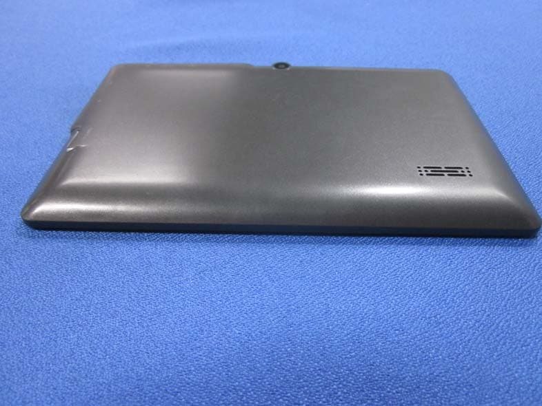
Z75TB6502G PHONE TABLET PC
DORRY ELECTRONICS INTERNATIONAL CO.,LTD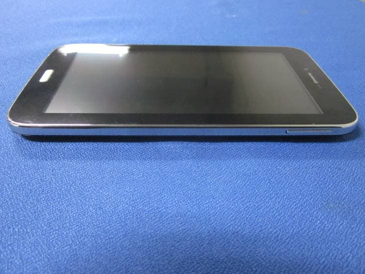
Click to zoom
Application Details
- Equipment Class
- DSS - Part 15 Spread Spectrum Transmitter
- Date of Grant
- Jan 12, 2014
- Application Purpose
- Original Equipment
- Date of Application
- Jan 12, 2014
- Equipment Note
- 2G PHONE TABLET PC
- Frequency Range
- 2402.00000000 - 2480.00000000
- Country
- China
Documents & Files
Document Text
Text extracted from the exhibit documents filed with the FCC. Open a document above to read the original.
Users Manual
2G Phone Tablet PC User Guider TB-650 Please read the documentation 1. Before using the equipment, please read these instructions carefully to ensure safe and proper use. 2. The description is based on the factory setting. 3. Images and screen shots used in this manual may be different from the actual product appearance. 4. Available features and additional services may be changed by device, software, or service provider. 5. We’re not liable on the problems caused by a third-party applications. DORRY ELECTRONICS INTERNATIONAL CO.,LTD Power button Long press:turn on/shutt down,restart to confirm Short press: turn off and to lock the screen,and let the phones sleeping ; to press the button again to restart the screen Volume button To adjust the volume of the device Home key To press it, the device will return to standby screen RESET Reset Main Screen The main screen can be viewed after unlocked. you can see the indicator, widgets, application shortcuts and other items. The main screen extends to beyond the width of screen, you can switch to a different page by sliding your finger around on the desktop. 1 Open the search widget to search 2 System notification bar 3 Open the application list and widget list 4 Slide left and right to switch to a different page Customized the Home Screen In the upper right corner of the main screen, the interface of application icons can be entered. The required application or small component can be clicked by sliding left and right on the main screen, until it’s shown on the main screen and drag to the special address required, then released. If you want to delete one item, please tap, hold and drag it into the position marked “the fork”. System Bar At the top of screen, there are some regular main buttons another side, such as “return”,”HOME”,”menu”,ect. To touch anyone to perform itself function well. The battery level, network signal, time and other icons are showing on the right side. You can view the notification by touching every one. Tips and Status Icons icon definition icondefinition Wi-Fi available around here Flight mode is activated Wi-Fi connected New mail The strength of signal New SMS or MMS Roaming On the phone Uploading data Missed call Downloading data Connected Connected to the computer Call forwarding is activated Bluetooth function is activated Alarm clock has started Battery charge SIM card is not inserted Rotating touch screen The device has been built-in motion sensors and rotary device. the interface will automatically rotate based on device orientation. If you need the interface remains the same direction, Please touch the right of system tray to turn off the automatically rotate setting. Unlock or lock the touch screen Tap and hold the screen lock screen icon, then drag it to the unlocked position to unlock the screen; If you have to lock the screen by hand, Please press the power button. Input text You can use the onscreen keyboard to write. Please tap the input area to open the on-screen keyboard , tap the “close” on the taskbar to turn it off ; If you need to switch the input method, please tap the key point intraday; You can copy and paste to input text quickly. Customized Equipment To select settings from the application list or the notifications panel, you can modify all settings as needed. Management Applications To select settings from application list Æenter to applications 1. if you want to uninstall the applications downloaded, you can click the “download”, select the desired application, and then click "Uninstall." 2. To pause the application, change the settings, or manage other options, select "All" or "running." Click a program, and then select the desired operation. Security Setting You can adopt a variety of ways to protect your equipment and information, such as the lock screen, encryption tablet computers. 1. Lock screen Select “settings” in the application list -> Security -> Screen lock: a. No: Never lock the screen b. Slide: no pattern, PIN or password to unlock the screen; c. Voice unlock: Set voice commands. Then set up a backup unlock d. PIN code: require digital PIN code to unlock the screen. After set up, when requiring the PIN code, enter it to unlock the screen. e. Pattern: require pattern to unlock. According to the mention on the screen to draw the same pattern you set, it will be unlock after successfully drawn f. Password: Need a password to unlock the screen. When the device asking password,Please enter the password you set to unlock Encrypt Tablet PC You can encrypt your accounts, settings, applications downloaded and the data, media and other files. After done, you will have to enter numeric PIN or password every time to decrypt the device. Reset Tablet PC To select “settings ” in the application list -> Backup and Reset -> Restore factory settings, you can restore the tablet to factory setting state and erase all data stored in the device. WARNING: This operation will delete all applications and files downloaded, and all personal information. Once these are deleted, they can not be restored. Communication Dial To tap the icon of dial in the application Call Several methods to do the call 1. dialing: input the phone number and tap the button of dial 2. call records: tap the number recorded in the mid-list 3. contact: Tap a contact to call the contact number Answer the call Press the circle button and slide it to the green position to answer the call. Reject or cut a call Press the circle button and slide it to the red position to reject an incoming call; To touch the midpoint to hang up. Use other functions. Tap the menu button on the right corner and select the “setting” to use the following functions: 1. fixed dialing: after set up the fixed dialing function, only the numbers fixed in the list can be dialed, others not. 2. quick reply: after set it up, when it’s not convenient to answer the phone, the quick reply phrases can be sent to the caller soon. 3. voicemail service: select or set up your…
Text truncated - open the document above for the full version.
Block Diagram
123456 A B C D 654321 D C B A Title NumberRevisionSize B Date:2-Jan-2014 Sheet of File:F:\M6502.DDBDrawn By: AP MT8312 PMU MT6323 RF AP6690 andriod LCD TP AW5208 transceiver MT6166 Battery GSM_WCDMA_ANT MT6627 GPS,WIFI,FM,Bluetooth ANT WIFI/GPS/BT MT8193 FN5401 Charg&OTGUSB CONNECTOR Camera G-Sensor MMA7660Powerkey Reset KEY VOL+ KEY VOL- KEY earhpone FM speaker MIC DDR3 EMMC T-FLASH SIM1 26MHZ 26MHZ 26MHZ SIM2 Receiver M6502
Cover Letter(s)
DORRY ELECTRONICS INTERNATIONAL CO., LTD F/2, 3-4 Lane, Guangya Yuan, Bantian Town, Longgang District, Shenzhen City, China Tel: +86-755-61216582 Fax: +86-755-61216978 DOC ATTESTATION LETTER FCC ID: Z75TB650 Date: Jan. 07, 2014 Federal Communications Commission Authorization and Evaluation Division 7435 Oakland Mills Road Columbia, MD 21046 To whom it may concern: I, the undersigned, hereby attest to the fact that I will apply the Declaration of Conformity procedure to the personal computer parting of. I understand the following FCC requirements: 1. Devices subject to the DoC procedure are required to be tested to show compliance with the FCC technical regulations by a recognized accredited testing laboratory. The testing laboratory must be accredited by a Commission approved accreditation body or designated under the terms of a government-to-government Mutual Recognition Agreement (MRA). A listing of those accredited testing laboratories that have been recognized by the Commission is published on the FCC Webpage: https://apps.fcc.gov/oetcf/eas/reports/TestFirmSearch.cfm (Select the "accredited" option to search for FCC recognized accredited test firms.) 2. Test facilities located in countries, where the U.S. does not have an operational Telcom MRA are not recognized by the FCC to test for the DoC procedure. 3. Pt 2.1077 contains the list of information that must be included in the Declaration of Conformity, which must be supplied with each product sold. The DoC compliance info shall be included in the User’s Manual or as a separate sheet. The info must contain the name, address, and phone number of the responsible party, which must be located within the United States. According to 2.909(c)(2), the responsible party is either the Manufacturer or if the product is imported the Importer. Sincerely, Kelvin Lian/General Manager
Cover Letter(s)
DORRY ELECTRONICS INTERNATIONAL CO., LTD F/2, 3-4 Lane, Guangya Yuan, Bantian Town, Longgang District, Shenzhen City, China Tel: +86-755-61216582 Fax: +86-755-61216978 Model Cover Letter FCC ID: Z75TB650 Date: Jan. 07, 2013 Federal Communications Commission Authorization and Evaluation Division 7435 Oakland Mills Road Columbia, MD 21046 To whom it may concern: To whom concern: The device (Product Name: 2G Phone Tablet PC) Models Name: TB-650, TB-726G, TB-782G, TB-M77, TB-798M, TB-677M, TB-720M, TB-A31G have same electrical, PCB and BOM, only the model’s name is different for marketing requirements. Sincerely, Kelvin Lian/General Manager
Cover Letter(s)
DORRY ELECTRONICS INTERNATIONAL CO., LTD F/2, 3-4 Lane, Guangya Yuan, Bantian Town, Longgang District, Shenzhen City, China Tel: +86-755-61216582 Fax: +86-755-61216978 AGENCY AUTHORIZATION LETTER FCC ID: Z75TB650 Date: Jan. 07, 2014 Federal Communications Commission Authorization and Evaluation Division 7435 Oakland Mills Road Columbia, MD 21046 To whom it may concern: We, the undersigned, hereby authorize Shenzhen CTL Electromagnetic Technology Co., Ltd.(MR. Tracy Qi) on our behalf, to apply to the Federal Communications Commission on our equipment. Any and all acts carried out by Shenzhen CTL Electromagnetic Technology Co., Ltd. (MR. Tracy Qi) on our behalf shall have the same effect as acts of our own. This authorization expires on Jan. 06, 2015. This is to advise that we are in full compliance with the Anti-Drug Abuse Act. We, DORRY ELECTRONICS INTERNATIONAL CO., LTD are not subject to a denial of federal benefits pursuant to Section 5301 of the Anti-Drug Act of 1988, 21 USC853a, and no party to the application is subject to a denial of federal benefits pursuant to that section. Sincerely, Kelvin Lian/General Manager
ID Label/Location Info
FCC ID Label Information 1. Label location: 2. FCC ID Label: DORRY ELECTRONICS INTERNATIONAL CO.,LTD 2G Phone Tablet PC Model: TB-650 FCC ID: Z75TB650 This device complies with Part 15 of the FCC Rules. Operation is subject to the following two conditions: (1) this device may not cause harmful interference, and (2) this device must accept any interference received, including interference that may cause undesired operation.
Operational Description
Operation Description Model: TB-650 Band: GSM850,GSM900,DCS1800,PCS1900 1. Scope This document shows and provides the basic information about the platform we used.The more detail information about RF section are also included. M6502 product is new Pad designe by HXMID .The baseband circuit is base on MTK MT8312 and RF circuit is included Transceiver named MTK MT6166 , AP PA and skyworks PA,It works at five bands,GSM850,GSM900,DCS1800,PCS1900 2. Platform MT8312 is based on RF band support GSM+GNSS+wifi+Bluetooth+FM. The package supports dual-channel DDR3 using BGA package and EMMC flash device through SDIO interface. The GNSS+WIFI+Bluetooth +FM is MT6627 core. -Baseband functions,including mulitipe hareware cores -Single platform that provides dedicated support for all mardet leading codecs and other multimedia formats to support carrier deploymetnts around the word. -High-quality digital still image camera performance with up to 5-megarpixel resolution -HS-USB and OTG-USB core with built-in PHY eliminates additional USB components. -DC power reduction using innovative technique -integarates multiple processors -Supported two high speed DDR3 IC. 3.Tansceiver MT6166 The MT6166 is a RF transceiver targeted at high speed 2G multi-mod smart phone and tablet computers implanted in 40nm CMOS,The RF transceiver function is fully integrated. The document briefly introruces the RF mocros in MT6166 3. PA GSM AP6690 U616 is a transmit and receive Front End Module(FEM) designed is very low profile(0.9mm) and compact for factor for quad-band cellular handsets GSM850/GSM900/DCS1800/PC1900 operation –a complete transmit vco-to – Antenna and Antenna-to-receiver SAW filter solution.The FEM also supports Class 12 General Packet Radio Service(GPRS) multi-slot operation. Modes of operation: Operating Parameters WIFI/BT/FM/GPS operation block: MT6627
Schematics
5 5 4 4 3 3 2 2 1 1 DD CC BB AA check MSDC1/2 IO power C115 close to pin E1 (150mil) C125 close to pin G26 (150mil) VCCK_VPROC VCCK To MT6323 VPROC_FB pin (1)VPROC_BB, GND pin of 1st cap group should be laid differential pair with ground shielding remote sense to PMIC To MT6323 GND_VPROC_FB pin (2)R107 & R103 must be close to 1st cap group. If you want to remove them, please make sure the VPROC_FB/GND_VPROC_FB must connect from 1st cap. group of VPROC 1.35V for DDR3L 1.5V for DDR3 DDR3VCCIO VTCXO_PMU VIO18_PMU VIO18_PMU VIO18_PMU VUSB_PMU VIO18_PMU VIO18_PMU VMC_PMU VIO18_PMU VPROC_PMU VIO18_PMU VIO18_PMU VIO28_PMU VM_PMU DDR3VCCIO DDR3VCCIO VPROC_FB3 GND_VPROC_FB3 Title SizeDocument Number Rev Date:Sheet of MT8382 TABLET V1.0 01 MT8382 - Power C 122Thursday, January 02, 2014 Title SizeDocument Number Rev Date:Sheet of MT8382 TABLET V1.0 01 MT8382 - Power C 122Thursday, January 02, 2014 Title SizeDocument Number Rev Date:Sheet of MT8382 TABLET V1.0 01 MT8382 - Power C 122Thursday, January 02, 2014 C132 10uF/C0603 2 1 C151 100nF/C0402 2 1 C104 100nF/C0402 2 1 C148 100nF/C0402 2 1 C112 100nF/C0402 2 1 C117 100nF/C0402 2 1 C131 100nF/C0402 2 1 C110 100nF/C0402 2 1 C125 100nF/C0402 2 1 C113 100nF/C0402 2 1 C109 100nF/C0402 2 1 C145 100nF/C0402 2 1 C111 100nF/C0402 2 1 C129 10uF/C0603 2 1 C133 10uF/C0603 2 1 C143 100nF/C0402 2 1 C140 100nF/C0402 2 1 C116 100nF/C0402 2 1 C156 100nF/C0402 2 1 C108 100nF/C0402 2 1 MT8382 U201B DVSS A19 DVSS A26 DVSS B4 DVSS B10 DVDD12_EMI E7 DVDD12_EMI F7 DVDD12_EMI F8 DVDD12_EMI G8 AVSS18_MD U20 AVSS18_WBG U7 AVSS18_WBG V7 AVSS18_MD U21 DVSS B12 DVSS B14 DVSS B17 DVSS B22 DVSS B24 DVSS C4 DVSS C8 DVSS C11 DVSS C12 DVSS C16 DVSS C17 DVSS C18 DVSS C20 DVSS C21 DVSS C22 DVSS C23 DVSS C25 DVSS D4 DVSS D5 DVSS D7 DVSS D9 DVSS D11 DVSS D13 DVSS D15 DVSS D17 DVSS D21 DVSS D24 DVSS E5 DVSS E8 DVSS E10 DVSS E18 DVSS E21 DVSS F6 DVDD28_MSDC1 E1 DVDD28_MSDC2 V1 DVDD28_BPI AD26 DVDD28_MD U25 DVDD18_IO1 Y26 DVDD18_IO2 D1 DVDD18_IO3 W1 DVDD18_IO4 AG13 AVSS18_WBG W7 AVSS18_WBG Y7 AVSS18_WBG AB6 AVSS18_WBG AB8 AVSS18_WBG AC3 VCCK L11 VCCK L12 VCCK L13 VCCK L14 VCCK L15 VCCK L16 VCCK L17 VCCK M10 VCCK M18 VCCK N10 VCCK N18 AVDD18_MD AE21 AVSS18_MD V20 AVSS18_MD V21 AVDD18_AP AE19 AVDD28_DAC AE22 DVDD18_PLLGP AE18 AVDD18_MEMPLL A3 AVSS18_MEMPLL A2 DVDD18_MIPITX L2 DVDD18_MIPIIO G1 AVDD33_USB T24 AVDD18_USB P26 AVSS33_USB R24 DVDD12_EMI G9 DVDD12_EMI G11 DVDD12_EMI G13 DVDD12_EMI G15 DVDD12_EMI G16 DVDD12_EMI G18 DVDD12_EMI H8 DVSS F18 DVSS18_MIPIIO H4 DVSS18_MIPITX L4 DVDD12_EMI H11 DVDD12_EMI H13 DVSS G6 DVSS G7 DVSS G14 DVSS G17 DVSS G20 DVSS H10 DVSS L10 DVSS L18 DVSS M12 DVSS M13 DVSS M14 DVSS M15 DVSS M20 DVSS N11 DVSS N21 DVSS P10 DVSS P11 DVSS P12 DVSS P13 DVSS P16 DVSS P17 VCCK P9 VCCK P18 VCCK R9 DVDD18_IO0 L26 DVSS P21 VCCK R10 AVSS18_MD W20 DVDD12_EMI H15 DVDD12_EMI H16 DVDD12_EMI H18 DVDD18_MSDC0 G26 VCCK R18 DVSS R2 DVSS R11 DVSS T11 AVSS18_WBG AC5 AVSS18_WBG AC7 AVSS18_WBG AD4 AVSS18_WBG AE3 AVSS18_MD W21 AVSS18_MD Y20 AVSS18_MD Y21 AVSS18_MD AA21 AVSS18_MD AB21 AVSS18_AP U17 AVSS18_AP U18 AVSS18_WBG AE5 DVSS T13 DVSS T16 DVSS T17 DVSS T18 DVSS T21 DVSS M11 DVSS U11 DVSS U12 DVSS V11 DVSS V12 DVSS V13 DVSS M16 DVSS K21 DVSS M17 DVSS H12 DVSS J21 DVSS H20 DVSS H17 DVSS H14 VCCK_VPROC N12 VCCK_VPROC N13 VCCK_VPROC N14 VCCK_VPROC N15 VCCK_VPROC N16 VCCK_VPROC N17 VCCK_VPROC P14 VCCK_VPROC R15 VCCK_VPROC P15 VCCK_VPROC R14 VCCK_VPROC R13 VCCK_VPROC R12 VCCK_VPROC R16 VCCK_VPROC R17 VCCK_VPROC T14 VCCK_VPROC T15 VCCK T10 VCCK U10 VCCK V10 VCCK_VPROC U15 VCCK_VPROC U16 VCCK_VPROC V15 VCCK_VPROC V16 AVSS18_MD AC21 AVSS18_MD AD22 AVSS18_MD AG26 AVSS18_AP V17 AVSS18_AP V18 AVSS18_AP AA18 AVSS18_AP AB19 AVSS18_WBG AF3 AVSS18_WBG AG1 DVSS18_MIPIIO H5 DVSS18_MIPIIO J5 DVSS18_MIPIIO J7 DVSS18_MIPITX M7 DVSS18_MIPITX M8 DVSS18_MIPITX N3 DVSS T12 DVSS V14 C130 4.7uF/C0603 2 1 C153 10uF/C0603 2 1 C123 100nF/C0402 2 1 C157 100nF/C0402 2 1 C128 100nF/C0402 2 1 C142 100nF/C0402 2 1 C158 100nF/C0402 2 1 C138 100nF/C0402 2 1 C134 10uF/C0603 2 1 C127 100nF/C0402 2 1 C152 1uF/C0402 2 1 R1660NC/R0402R0402 R329 0R/nc 12 C124 100nF/C0402 2 1 C144 100nF/C0402 2 1 R16640R/R0402R0402 C120 100nF/C0402 2 1 R16650R/R0402 R327 0R/nc 12 C122 100nF/C0402 2 1 C136 10uF/C0603 2 1 C155 1uF/C0402 2 1 C119 1uF/C0402 2 1 C115 100nF/C0402 2 1 5 5 4 4 3 3 2 2 1 1 DD CC BB AA Close to MT8382 C213 Close to MT8382 AF19 should connect to C213.2 first, than connect to GND by via 90 Ohm differential Close to MT8382 MT6605 OSC_EN (SRCLKENAI) Need to default low for MT6605 TESTMODE boot-strap I2C0 : CTP I2C1 : MT6333 / Main Camera / Sub Camera I2C2 : G/M/GYRO/ALS sensor UART0: Debug UART1: Debug UART2: Debug UART3: Debug MSDC0 : eMMC MSDC1 : T-Card MSDC2 : N/A EINT0 : MT6333 EINT1 : N/A EINT2 : N/A EINT3 : EINT4 : EINT5 : NFC EINT6 : CTP EINT7 : NFC EINT8 : EINT9 : EINT14 : EINT18 : I2C0: CTP, MT8193 I2C1: PMIC, CHARGER, CAMERA I2C2: NFC, SENSOR R1659 close to R1662 3G --> R1659 WIFI --> R1662 2.8V GPIO EVREF MIPI_VRT CLK26M RTC32K_CK REFP USB_VRT UTXD1 URXD1 UTXD0 URXD0 DPI_CK BSI_DATA1 BSI_DATA0 BSI_EN BSI_CLK BSI_DATA2 DL_I_N DL_Q_P DL_Q_N DL_I_P UL_I_N UL_Q_P UL_Q_N UL_I_P DPI_VSYNC DPI_HSYNC TESTMODE FSOURCE_PFSOURCE_P REXTDN EA15 EA14 EA13 EA12 EA11 EA10 ED3 ED2 ED1 ED0 ED15 ED14 ED12 ED13 ED10 ED11 ED6 ED5 ED4 ED9 ED7 ED8 EA9 EA1 EA2 EA3 EA4 TP_MEMPLL EA5 EA6 EA7 EA8 EA0 DDR3VCCIO VIO18_PMU VIO18_PMU VIO18_PMU EVREF2,6 SCL012,14,2 SDA012,14,2 SCL115,2,4 SDA115,2,4 SDA216,17,2 SCL216,17,2 CMMCLK15 WATCHDOG_B3 RTC32K_CK12,3 SIM1_SCLK3 SIM1_SRST3 CHD_DP3 CHD_DM3 USB_DP19 USB_DM19 MC1DA118 MC1DA018 MC1DA218 MC1DA318 eMMC_DAT06 eMMC_DAT26 eMMC_DAT36 eMMC_DAT16 eMMC_DAT66 eMMC_DAT76 eMMC_DAT46 eMMC_DAT56 MC1CK18 MC1CM18 eMMC_CLK6 eMMC_CMD6 eMMC_RST6 SIM1_SIO3 URXD121 UTXD121 URXD021 UTXD021 MCU_JTCK21 MCU_JTDO21 MCU_JTDI21 MCU_JTMS21 DPI_CK12 SCL216,17,2 SDA012,14,2 SDA216,17,2 SDA115,2,4 SCL012,14,2 SCL115,2,4 PWM13 PMIC_SPI_MOSI3 PMIC_SPI_MISO3 PMIC_SPI_SCK3 PMIC_SPI_CS3 EINT_PMIC3 BSI-A_DAT27 BSI-A_DAT17 BSI-A_…
Text truncated - open the document above for the full version.
Test Report
Shenzhen CTL Electromagnetic Technology Co., Ltd. Tel: +86-755-89486194 Fax: +86-755-26636041 FCC PART 15 SUBPART C TEST REPORT FCC Part 15.247 Report Reference No......................: CTL1312121961-WB Compiled by ( position+printed name+signature)..: File administrators Jacky Chen Name of the organization performing the tests ( position+printed name+signature)..: Test Engineer Tracy Qi Approved by ( position+printed name+signature)..: Manager Tracy Qi Date of issue.....................................: Dec. 28, 2013 Representative Laboratory Name.: Shenzhen CTL Electromagnetic Technology Co., Ltd. Address.............................................: Floor 1-A, Baisha Technology Park, No.3011, Shahexi Road, Nanshan District, Shenzhen, China 518055 Test Firm..........................................: Bontek Compliance Testing Laboratory Ltd Address.............................................: 1/F, Block East H-3, OCT Eastern Ind. Zone, Qiaocheng East Road, Nanshan, Shenzhen, China Applicant’s name............................: DORRY ELECTRONICS INTERNATIONAL CO.,LTD Address.............................................: F/2, 3-4 Lane, Guangya Yuan, Bantian Town, Longgang District, Shenzhen City, China Test specification: Standard ...........................................: FCC Part 15.247: Operation within the bands 902–928 MHz, 2400– 2483.5 MHz, and 5725–5850 MHz. Master TRF.......................................: Dated 2011-01 Shenzhen CTL Electromagnetic Technology Co., Ltd. All rights reserved. This publication may be reproduced in whole or in part for non-commercial purposes as long as the Shenzhen CTL Electromagnetic Technology Co., Ltd. is acknowledged as copyright owner and source of the material. Shenzhen CTL Electromagnetic Technology Co., Ltd. takes no responsibility for and will not assume liability for damages resulting from the reader's interpretation of the reproduced material due to its placement and context. Test item description ....................: 2G Phone Tablet PC FCC ID.......................................: Z75TB650 Trade Mark .......................................: N/A Model/Type reference.......................: TB-650, TB-726G, TB-782G, TB-M77, TB-798M, TB-677M, TB-720M, TB-A31G GSM Transmit ...........................................: GSM 850: 824~849MHz, PCS 1900: 1850~1910MHz Receive ............................................: GSM 850: 869~894MHz, PCS 1900: 1930~1990MHz Release Version .............................: R99 Type of modulation ...........................: GMSK for GSM/GPRS 8PSK for EDGE V1.0 Page 2 of 106 Report No.: CTL1312121961-WB GPRS Type ......................................: Class B GPRS Class ...................................: Class 12 Bluetooth Work frequency................................: 2402~2480MHz Version..............................................: V3.0 + HS Type of modulation ...........................: FHSS Data Rate..........................................: 1Mbps(GFSK), 2Mbps(Pi/4 DQPSK), 3Mbps(8DPSK) Wi-Fi Work frequency ................................: 802.11b/g/n(20MHz): 2412~2462MHz Type of modulation ...........................: 802.11b DSSS, 802.11g/n: OFDM Data Rate..........................................: 802.11b: 1/2/5.5/11 Mbps 802.11g: 6/9/12/18/24/36/48/54 Mbps 802.11n: up to 65 Mbps Antenna Gain ...................................: 0 dBi for GSM850 and PCS1900 -2.0 dBi for Bluetooth and Wi-Fi Antenna type ....................................: Internal Result................................................: Positive V1.0 Page 3 of 106 Report No.: CTL1312121961-WB T E S T R E P O R T Test Report No. : CTL1312121961-WB Dec. 28, 2013 ______________________________________________________________________________________________ Date of issue Equipment under Test : 2G Phone Tablet PC Model /Type : TB-650 Listed Models : TB-726G, TB-782G, TB-M77, TB-798M, TB-677M, TB-720M, TB-A31G Different Description : Only model’s name and colour are different based on marketing requirement. Applicant : DORRY ELECTRONICS INTERNATIONAL CO.,LTD Address : F/2, 3-4 Lane,Guangya Yuan,Bantian Town, Longgang District, Shenzhen City, China Manufacturer : DORRY ELECTRONICS INTERNATIONAL CO.,LTD Address : F/2, 3-4 Lane,Guangya Yuan,Bantian Town, Longgang District, Shenzhen City, China Test Result according to the standards on page 5: Positive The test report merely corresponds to the test sample. It is not permitted to copy extracts of these test result without the written permission of the test laboratory. V1.0 Page 4 of 106 Report No.: CTL1312121961-WB Contents 1. TEST STANDARDS .................................................................. 5 2. SUMMARY............................................................................. 6 2.1. General Remarks 6 2.2. Equipment Under Test 6 2.3. Short description of the Equipment under Test (EUT) 6 2.4. EUT operation mode 6 2.5. EUT configuration 7 2.6. Configuration of Tested System 7 2.7. Related Submittal(s) / Grant (s) 7 2.8. Modifications 7 2.9. NOTE 7 2.10. Frequency Hopping System Requirements 8 2.11. Mode of Operation 10 3. TEST ENVIRONMENT.............................................................. 11 3.1. Address of the test laboratory 11 3.2. Test Facility 11 3.3. Environmental conditions 11 3.4. Statement of the measurement uncertainty 11 3.5. Test Description 12 3.6. Equipments Used during the Test 13 4. TEST CONDITIONS AND RESULTS ............................................ 14 4.1. AC Power Conducted Emission 14 4.2. Radiated Emission 17 4.3. Maximum Peak Output Power 24 4.4. 20dB Bandwidth 31 4.5. Band Edge 38 Radiated Test: 43 4.6. Frequency Separation 67 4.7. Number of hopping frequency 74 4.8. Time Of Occupancy(Dwell Time) 83 4.9. Spurious RF Conducted Emissions 89 4.10. Antenna Requirement 96 4.11. RF Exposure 97 5. TEST SETUP PHOTOS OF THE EUT .......................................... 98 6. EXTERNAL AND INTERNAL PHOTOS OF THE EUT ..................... 100 V1…
Text truncated - open the document above for the full version.
Test Setup Photos
DSS Test Setup Photos of the EUT
Contact Information
Applicant
Kelvin Lian(General Manager)
Test Firm
Bontek Compliance Testing Laboratory LtdTony Wu
Technical Specifications
| # | Rule Parts | Frequency Range | Power Output |
|---|---|---|---|
| 1 | 15C | 2.40 GHz - 2.48 GHz | 6.00 mW |
Other Applications from DORRY ELECTRONICS INTERNATIONAL CO.,LTD
Z75Q88
Mar 04, 2014TABLET PC
Equipment Class
DTS - Digital Transmission System
Z75-N1001
Nov 08, 201110.1" LAPTOP
Equipment Class
JBP - Part 15 Class B Computing Device Peripheral