Z9I-MD-H01MM CHIP DEDICATED READER WRITER MODULE
Senstech Sdn. Bhd.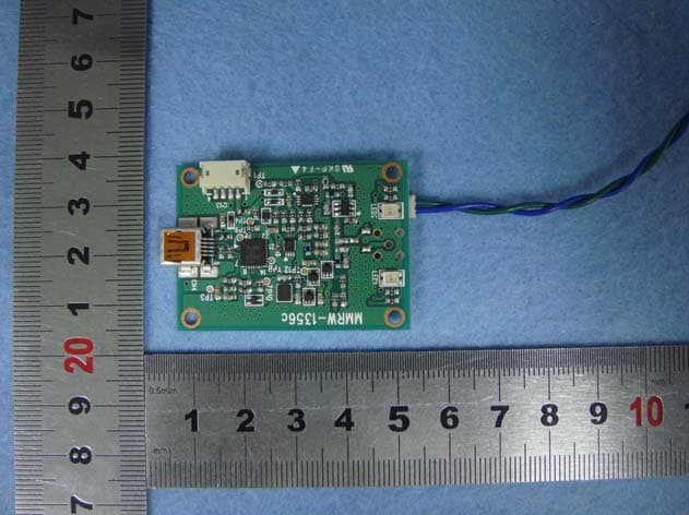
Click to zoom
Application Details
- Equipment Class
- DXX - Part 15 Low Power Communication Device Transmitter
- Date of Grant
- Dec 11, 2011
- Application Purpose
- Original Equipment
- Date of Application
- Dec 11, 2011
- Equipment Note
- MM CHIP DEDICATED READER WRITER MODULE
- Frequency Range
- 13.56000000 - 13.56000000
- Company
- Senstech Sdn. Bhd.
- Country
- Malaysia
Documents & Files
Document Text
Text extracted from the exhibit documents filed with the FCC. Open a document above to read the original.
Users Manual
1/17 MMRW User Manual Product Name MM Chip Reader / Writer module [13.56MHz] Product Number MMRW-MD-H01 FEC International (M) SDN BHD 2 nd Nov. 2011 2/17 Contents 1 Introduction ............................................................................. 3 2 Usage Important Points ...................................................................... 3 3 Key features ............................................................................... 3 4 Reader/writer module package content............................................................ 4 5 Connections ............................................................................... 5 6 Function and use ............................................................................ 5 7 Hardware ................................................................................. 6 7.1 Carrier oscillation circuit, ASK modulator circuit, transmission output circuit .......................... 6 7.2 RF receiving circuit ..................................................................... 7 7.3 Microprocessor ......................................................................... 8 7.4 Microprocessor’s pin assignment ........................................................... 9 7.5 RF antenna ............................................................................ 9 8 Firmware ................................................................................ 10 9 Firmware Writing Procedures ................................................................. 11 9.1 Firmware writing application start-up and installation ........................................... 11 9.2 Firmware writing ...................................................................... 11 10 Product general specification .................................................................. 14 11 Annexes ................................................................................. 15 11.1 Schematics ........................................................................... 15 11.2 List of components ..................................................................... 16 11.3 Antenna layout ........................................................................ 17 12 FCC STATEMENT ......................................................................... 17 3/17 1 Introduction This MMRW-MD-H01 is a reader/writer module complied with multiband RFID chip dubbed as “MM Chip”. This document contains the instructions to use and evaluate the functions and the performance of this device. For external interface connection, either USB or UART serial connection can be applied, which is applicable to almost all of the controller systems. For more details on the product specifications, please refer to “MMRW-H01 Product Specification Document”. 2 Usage Important Points [Regulation/Standards] This product follows the guidance for reading/writing communication equipment. It is important to check the regulation/standard and the seller or user of the intended country. [Points to take notes before using the product] 1) This product is designed for general use and should not be utilized with application such as medical appliances related to human life or in space satellite environment which requires high reliability. Our company will not be responsible for any accidents caused from the said events, such as personal accident, fire accident or any public related accident. 2) This product is emitting radio wave which can affect medical appliances such as the pacemaker device. 3) Do not place this product near any radio device since it can cause interference. 4) Do not touch the connector terminal as it can result in electrical shock and will eventually destroy the product. 3 Key features Support MM2 chip air interface protocol and commands Light weight, compact size module UART serial and USB communication available RF output: 25mW Operation voltage: 5VDC 4/17 4 Reader/writer module package content [RFID reader / writer board: MMRW-MD-H01] USB (Mini B) Packet communication complies with USB2.0/1.1 UART serial Communication speed Variable according to a command (default:9,600bps) (1,200/2,400/4,800/9,600/19,200/38,400/57,600bps) Data bit: 8bit Stop bit: 1bit Parity bit: N/A Flow control: N/A [Board antenna: MMATH-4570] [CD with SDK and documentation] Included in the CD are SDK and related documents, product specifications and various manuals. For more details, please see “readme.txt” included in the CD. 5/17 5 Connections The first step is to connect the components. Connect antenna board to the RFID reader / writer board using the connector. Terminal and reader/writer can be connected by USB or UART serial port. Pin assignment for UART serial is stated in the table below. Please prepare a harness cable for the connection to device terminal. No. Signal name I/O Content 1 VCC - Provide DC 5V (+/-0.25V) 2 GND - GND 3 TXD OUT UART serial signal output (LV-TTL) 4 RXD IN UART serial signal input (LV-TTL) [Pin assignment] 6 Function and use The equipment is ready to be operated once all connections are completed. Next, equipment operating with SDK package will be explained. SDK Package is prepared for application development of MMRW series. SDK Package contains demo software, USB driver, USB communication library, and sample source code. For further details, please refer to “Demo Software Manual” before using MMRW demo software. Please refer to “MMRW Command Library Function Specification” to develop application. 6/17 7 Hardware 7.1 Carrier oscillation circuit, ASK modulator circuit, transmission output circuit Fig. 1 shows carrier oscillation circuit, ASK modulator circuit and transmission output circuit. 13.56MHz carrier (waveform ①) from U9 oscillation circuit is input to gate 1 of gate IC U2TC7S02. As for Gate2, on/off of the sending can be done by the waveform ② from U8-11P. U2 output (waveform ③) is input to inverter IC U1 TC7SZ04. U1 is a transmitting circuit, and Q1 is AS…
Text truncated - open the document above for the full version.
Block Diagram
1/2 Block diagram No.D07011R-A /F Product Name MM Chip Dedicated Reader/Writer Module [13.56MHz] Model MMRW-MD-H01 Document Name Block diagram Revision Nov. 2011 FEC Inc. 1414, Ustugi-machi Higashi Kanazawa-city, Ishikawa Prefecture 920-0377 TEL: 076-269-8890 / FAX: 076-269-8897 2/2 Block diagram No.D07011R-A /F Tr a n s m i t t e r Crystal oscillator: Crystal oscillator determines the carrier frequency 13.56MHz. Tr a n s m i t SW Receiver RF connector Final amplifier LPF AM modulat Drive amplifie Crystal oscillator (13.56MHz) Buffer amplifie AF amplifier RSSI detecto Comparator Controller (decryption) UART serial connector LED USB connecto r Power Each
Cover Letter(s)
Senstech Sdn. Bhd. Suite 10-01,Level 10, Menara Atlan, 161B Jalan Ampang, 50450 Kuala Lumpur, Malaysia FCC ID: Z9I-MD-H01 Gentlemen: Regarding to the FCC 15.212, Senstech Sdn. Bhd. would like to request modular approval for the submission FCC ID: Z9I-MD-H01. Senstech Sdn. Bhd. confirms that the product complies with numbered requirements identified below: 1. “The radio elements must have the radio frequency circuitry shielded.” The EUT Shielding was not needed because of the low field strength levels. 2. “The modular transmitter must have buffered modulation/data inputs” The EUT has buffered data inputs; it is integrated in chip C8051F321. 3. “The modular transmitter must have its own power supply regulation” The EUT interface provides 5.0VDC 4. “The modular transmitter must comply with the antenna and transmission system requirements of Sections 15.203, 15.204(b) and 15.204(c) ” The EUT meets the antenna requirements. It has a unique PCB antenna. Refer to the photo of antennas are shown in the test report. 5. “The modular transmitter must be tested in a stand-alone configuration.” The EUT is tested in a stand alone configuration via a Notebook. Please see the photo of test setup photo of the report. 6. “The modular transmitter must be labeled with it’s own FCC ID number.” The EUT has it’s own FCC ID and the label is visible. 7. “The modular transmitter must comply with any specific rule or operating requirements applicable to the transmitter and the manufacture must provide adequate instructions along with module to explain any such requirement.” The EUT is comply with all applicable FCC Rules. Warning detail refer to the user manual. 8. “The module must comply with RF exposure requirements” Since this EUT is being applied for approval under 15.209 there is no need to address the RF Exposure issue Sincerely, Senstech Sdn. Bhd. ------------------------------- Ida Semurni Abdullah Ali project manager
External Photos
SENSTECH SDN. BHD. MODEL: MMRW-MD-H01 APPENDIX B – External & Internal Photo EUT – Rear View 1 EUT - Rear View 2 REPORT NO.: MTI111102002RF SENSTECH SDN. BHD. MODEL: MMRW-MD-H01 EUT - Rear View 3 EUT - Rear View 4 REPORT NO.: MTI111102002RF SENSTECH SDN. BHD. MODEL: MMRW-MD-H01 EUT - Rear View 5 EUT - Rear View 6 REPORT NO.: MTI111102002RF
ID Label/Location Info
SENSTECH SDN. BHD. MODEL: MMRW-MD-H01 Proposed Label Location on EUT FCC ID Label Location REPORT NO.: MTI111102002RF
ID Label/Location Info
SENSTECH SDN. BHD. MODEL: MMRW-MD-H01 APPENDIX A - PRODUCT LABELING Proposed FCC ID Label Format FCC ID: Z9I-MD-H01 This device complies with Part 15 of the FCC Rules. Operation is subject to the following two conditions: (1) This device may not cause harmful interference, and (2) This device must accept any interference received, including interference that may cause undesired operation. Specifications : Text is Black in color and justified. Labels are printed in indelible ink on permanent adhesive silk-screened onto the EUT or shall be affixed at a conspicuous location on the EUT. REPORT NO. MTI111102002RF
Internal Photos
SENSTECH SDN. BHD. MODEL: MMRW-MD-H01 APPENDIX B – External & Internal Photo EUT – Rear View 1 EUT - Rear View 2 REPORT NO.: MTI111102002RF SENSTECH SDN. BHD. MODEL: MMRW-MD-H01 EUT - Rear View 3 EUT - Rear View 4 REPORT NO.: MTI111102002RF SENSTECH SDN. BHD. MODEL: MMRW-MD-H01 EUT - Rear View 5 EUT - Rear View 6 REPORT NO.: MTI111102002RF
Operational Description
MMRW functional descriptions MMRW mainly functions as a data transceiver device to an IC tag. 1. Connect the equipment as shown below. MMRW has serial interface and USB interface. Host controller MMRW-MD-H01 Antenna Serial or USB communicati 2. Power supply to the control board. 3. Wave the IC tag over an antenna surface 4. Send a command from the host controller. A power supply and data are transmitted to an IC tag from an antenna, and it communicates. IC Tag MMRW-MD-H01 Host controller Antenna 5. MMRW acquires the data of an IC tag and transmits the acquired data to a host controller.
Test Report
FCC Part 15.209 Measurement And Test Report For Senstech Sdn. Bhd. Suite 10-01,Level 10, Menara Atlan, 161B Jalan Ampang, 50450 Kuala Lumpur, Malaysia FCC ID: Z9I-MD-H01 Nov 26, 2011 This Report Concerns: Original Report Equipment Type: MM chip dedicated reader writer module Report Number: MTI111102002RF Test Engineer: Bill Chen Reviewed By: Jason Zheng Approved & Authorized By: Hebe Lee Test Date: Nov 4 - 25,2011 Prepared By: MTI Technology Laboratory Ltd. 10F, Yinxing Business Hotel, Xixiang Road, Bao'an District, Shenzhen, P,R.China. Tel: +86-755-8885 0135 Fax: +86-755-8885 0136 Note: This test report is limited to the above client company and the product model only. It may not be duplicated without prior written consent of MTI Technology Laboratory Ltd. . Report No.:MTI111102002RF Page 2 of 11 TABLE OF CONTENTS 1. GENERAL INFORMATION......................................................................................................................... 3 1.1 PRODUCT DESCRIPTION FOR EQUIPMENT UNDER TEST (EUT)........................................................................................3 1.2 RELATED SUBMITTAL(S) / GRANT (S) .............................................................................................................................3 1.3 TEST METHODOLOGY..................................................................................................................................................3 1.4 TEST FACILITY............................................................................................................................................................4 2. SYSTEM TEST CONFIGURATION............................................................................................................ 5 2.1 EUT CONFIGURATION..................................................................................................................................................5 2.2 EUT EXERCISE...........................................................................................................................................................5 2.3 GENERAL TEST PROCEDURES......................................................................................................................................5 2.4 LIST OF MEASURING EQUIPMENTS USED.......................................................................................................................6 3. SUMMARY OF TEST RESULTS................................................................................................................ 7 4. RADIATED EMISSION...............................................................................................................................8 4.1 LIMITS OF RADIATED EMISSION MEASUREMENT..............................................................................................................8 4.2 EUT SETUP................................................................................................................................................................8 4.3 TEST EQUIPMENT LIST AND DETAILS.............................................................................................................................8 4.4 TEST PROCEDURE.......................................................................................................................................................9 4.5 TEST RESULT..............................................................................................................................................................9 Report No.:MTI111102002RF Page 3 of 11 1. GENERAL INFORMATION 1.1 Product Description for Equipment Under Test (EUT) Applicant: Senstech Sdn. Bhd. Address of applicant: Suite 10-01,Level 10, Menara Atlan, 161B Jalan Ampang, 50450 Kuala Lumpur, Malaysia Manufacturer: FEC Inc Address of manufacturer: 1414 Higashi, Utsugi machi, Kanazawa shi, Ishikawa, 920- 0377, Japan Equipment Under Test: MM chip dedicated reader writer module Tested Model No.: MMRW-MD-H01 Trade Name: / Supplementary Models No: / Remark: supplementary models are only different in exterior with tested Model and with the same circuit construction Frequency range: 13.56 MHz Type of Modulation: ASK Number of Channels: 1 Antenna Type: Integral Antenna Power Supply: DC 5V Remark: * The test data gathered are from the production sample provided by the manufacturer. 1.2 Related Submittal(s) / Grant (s) This submittal(s) is a test report based on the Electromagnetic Interference (EMI) tests performed on the EUT. The EMI measurements were performed according to the measurement procedure described in ANSI C63.4 - 2003. The tests were performed in order to determine compliance with FCC Part 15, Subpart B, and section 15.205, and 15.209 rules. 1.3 Test Methodology Both conducted and radiated testing were performed according to the procedures in ANSI C63.4 - 2003, American National Standard for Methods of Measurement of Radio-Noise Emissions from Low-Voltage Electrical and Electronic Equipment in the range of 9 kHz to 40 GHz. Radiated testing was performed at an antenna to EUT distance 3 meters. Report No.:MTI111102002RF Page 4 of 11 1.4 Test Facility All measurement required was performed at laboratory of NTEK Testing Technology Co., Ltd., at 1/F, Building E, Fenda Science Park Sanwei Community, Xixiang Street, Baoan District , Shenzhen,Guangdong The test facility is recognized, certified, or accredited by the following organizations: FCC – Registration No.: 238937 NTEK Testing Technology Co., Ltd. EMC Laboratory has been registered and fully described in a report filed with the (FCC) Federal Communications Commission. The acceptance letter from the FCC is maintained in our files. Registration 238937. Report No.:MTI111102002RF Page 5 of 11 2. SYSTEM TEST CONFIGURATION The tests documented in this report were performed in accordance with ANSI C63.4-2003 and FCC CFR 47 Part 15 Subpart C. 2.1 EUT Configuration The EUT configuration for testing is instal…
Text truncated - open the document above for the full version.
Test Setup Photos
SENSTECH SDN. BHD. MODEL: MMRW-MD-H01 APPENDIX C - TEST SETUP PHOTOGRAPHS Radiation Emission Test Setup (30MHz to 1GHz) Radiation Emission Test Setup (Below 30MHz ) REPORT NO. MTI111102002RF
Contact Information
Applicant
Ida Semurni Abdullah Ali(project manager)
Test Firm
NTEK Testing Technology Co., Ltd.Wetow Huang
Technical Specifications
| # | Rule Parts | Frequency Range | Power Output |
|---|---|---|---|
| 1 | 15C | 13.56 MHz - 13.56 MHz | - |
Other Applications from Senstech Sdn. Bhd.
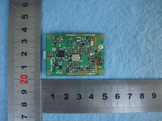
Z9I-MD-S01
Dec 07, 2011MM CHIP DEDICATED READER WRITER MODULE
Equipment Class
DXX - Part 15 Low Power Communication Device Transmitter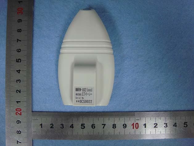
Z9I-U02
Dec 05, 2011MM CHIP DEDICATED READER WRITER
Equipment Class
DXX - Part 15 Low Power Communication Device Transmitter