ZBC-20WMS005Wireless Power Bank
SHENZHEN DNS INDUSTRIES CO., LTD.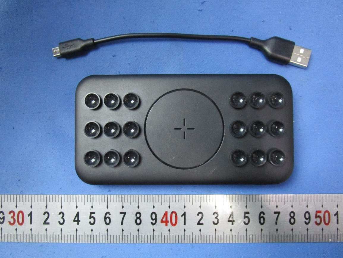
Click to zoom
Application Details
- Equipment Class
- DCD - Part 15 Low Power Transmitter Below 1705 kHz
- Date of Grant
- Jan 18, 2020
- Application Purpose
- Original Equipment
- Date of Application
- Jan 12, 2020
- Equipment Note
- Wireless Power Bank
- Frequency Range
- 0.11000000 - 0.20500000
- Country
- China
Documents & Files
Document Text
Text extracted from the exhibit documents filed with the FCC. Open a document above to read the original.
Users Manual
Welcome Thank you for purchasing this product. To ensure optimum performance and safety, please read these instructions carefully before operating the product. It is strongly recommended you keep the manual for future reference. Model No. WD-251A Product picture Description: 1. LED Indicator 2. Power Switch Button 3. USB Output 4. Micro USB Input Port Specification Product Name: Wireless Power Bank Battery Type: Li-Polymer Battery Input (Micro USB): DC5V 2A Wireless Output: 5W USB A Output: DC5V 2.1A Output: 10.5W Total Capacity: 5000mAh, 18.5Wh/3.7V iPad, Mobile Phones, iphone, iPod, and all other digital devices requiring charging through a DC 5.0V 1A or DC 5.0V 2.1A USB port. Note: (1).Both USB ports are of standard USB specification. (2).Support more than 85% of Samsung Tablets; Please use included “USB to Micro USB cable” to charge you device when your original cable not support this power bank. Hense the USB ports support all iPod, iPhone. Information Using your WD-251 Power Bank 1. You can use the included USB-Micro USB cable to charge the WD-251A Power Bank from a USB power source. Note: While the WD-251A Power Bank is being charged, the blue LEDs will flash and light up one after another. Once the Power Bank is fully charged, all LEDs will light up and the Power Bank will stop charging. You should be able to charge your mobile devices once the Power Bank completes its charging or disconnected from its power source. 2. Short press the on/off Power Switch Button on the Power Bank, the LEDs will be illuminated for 60 seconds and the power bank will start charging your ipad, mobile phone or any electronic devices. To stop charging your devices, simply disconnect them from the Power Bank. The Power output will remain for 60 seconds and stop automatically if the Power Bank does not start charging any device again within this period. Preparing to Wireless Charge: The Wireless charging Pad can charge Qi enabled smartphones. You can charge your smartphone with a protective case on it. (Works with most cases up to 4mm thick) If your protective cases has metallic studs, magnetic clasps, or a magnetic plate, you should remove the case before placing your phone on the mount, Also ensure the protective case does not create distance between the charging pad and the back of the phone that is greater that 4mm. Charging: Connect the Wireless Charging Pad using the includes USB to micro USB cable. Once plugged in, the blue LED light informs you that the mount is powered and ready to charge. Your smartphone will automatically begin to charge when placed on the Wireless Charging Pad. The green LED light indicates your smartphone is successfully charging. For optimum charging, place your mobile phone in the center of the charging pad. Adjust the viewing angle of the Wireless Charging Pad between flat or tilted by twisting the bottom of the pad. Battery Capacity Indicator & LED Light Switch Button The LED power indicators provide information about the battery charging status and battery power level: Press the Power Switch Button to check power level, the LED will be illuminated for 60 seconds. LED’s indicate from the right to left: ·1 LED Flashes:<5% Power ·1 LED on:<25% ·2 LEDs on:25%-50% ·3 LEDs on:50%-75% ·4 LEDs on:75%-100% It takes around 4 hours to fully charge this Power Bank via a 5V 2A USB power source. Maintenance In order to maximize the battery life, please maintain your WD-251A Power Bank as recommended below: 1. Re-charge your WD-251A Power Bank dry once every three months if it has not been in use. 2. Keep your your WD-251A Power Bank dry and away from moist or corrosive materials. 3. Do not wash the your WD-251A Power Bank with harsh chemicals, soaps or detergents. Package Contents -1X WD-251A Power Bank -1X USB Cable -1X User Manual Warning Read all instructions and warnings prior to using this product for the first time. Failure to read and follow these safety and usage instructions could result in fire, explosion, electric shock or other hazard that could potentially cause property damage or even fatal injure. 1. Do not modify, disassemble, open, drop, crush, puncture or shared the product 2. Do not expose the product to water or excessive moisture 3. Keep away from heat sources and direct sunlight to prevent heat build-up 4. Keep away from high voltage devices 5. This product is not a toy, keep away from children and ensure that all persons who use the product read and follow these instructions and warnings 6. Please do not try to charge your device when you are charging the power bank. FCC Compliance Statement This device complies with Part 15 of the FCC Rules. Operation is subject to the following two conditions: (1) this device may not cause harmful interference, and (2) this device must accept any interference received, including interference that may cause undesired operation. Warning: Changes or modifications to this unit not expressly approved by the party responsible for compliance could void the user’s authority to operate the equipment. NOTE: This equipment has been tested and found to comply with the limits for a Class B digital device, pursuant to Part 15 of the FCC Rules. These limits are designed to provide reasonable protection against harmful interference in a residential installation. This equipment generates, uses and can radiate radio frequency energy and, if not installed and used in accordance with the instructions, may cause harmful interference to radio communications. However, there is no guarantee that interference will not occur in a particular installation. If this equipment does cause harmful interference to radio or television reception, which can be determined by turning the equipment off and on, the user is encouraged to try to correct the interference by one or more of the following measures: - Reorient or relocate the receiving antenna. - Increase the separation between the equipment and receiver. - Connect the equipment into an …
Text truncated - open the document above for the full version.
Cover Letter(s)
SHENZHEN DNS INDUSTRIES CO., LTD. 2019-12-18 Federal Communications Commission 445 12 th Street SW Washington, DC 20554 Subject: Limited Agency Agreement SHENZHEN DNS INDUSTRIES CO., LTD. FCC ID: ZBC-20WMS005 To Whom It May Concern: We, SHENZHEN DNS INDUSTRIES CO., LTD. hereby authorized Intertek Testing Services to act as our Agent for the purpose of preparing application for FCC ID number ZBC-20WMS005 under all applicable parts of the FCC rules and regulations. The effective date of this limited agency agreement is 2019/12/18 The Limited Agency Agreement expires on 2023/12/31, unless sooner terminated or extended by written notice to Intertek Testing Services and the Federal Communications Commission. This is to advise that we are in full compliance with the Anti-Drug Abuse Act. The applicant is not subject to a denial of federal benefits pursuant to Section 5301 of the Anti-Drug Act of 1988, 21 U.S.C. 862, and no party to the application is subject to a denial of federal benefits pursuant to that section. If you have any questions or comments, please do not hesitate to contact me. Sincerely, Yuki Wu Certification Engineer
Cover Letter(s)
SHENZHEN DNS INDUSTRIES CO., LTD. Attention: Certification reviewer RE: Request for Confidentiality FCC ID: ZBC-20WMS005 To Whom It May Concern: Permanent Confidentiality [Complete this section if permanent confidentiality is requested] Request to withhold permanently from public review certain portions of the application for equipment certification for the referenced FCC identifiers. This request for confidentiality is made pursuant to 47 CFR 0.457(d) and 0.459 of the FCC Rules. In particular, the following sections of the application are to be kept permanently confidential: [Select one or more of items below, as appropriate] Schematics Block Diagrams Operational Description Tune-up Procedure Parts List Internal Photos (see note) Users Manual (see note) Note 1: Internal Photos may be held confidential 1) if the circuit board or internal components are not accessible to users. For example, it is acceptable if the circuit board is enclosed in epoxy. 2) Also, it is acceptable if the device is not accessible to the public, for example, a device mounted on the top of a large tower (or in a fenced enclosure) such that it is only serviceable by professional designated technicians under a Non-Disclosure Agreement (NDA). All sales for these devices must be under a NDA restricting the disclosure of the propriety information, including internal photos. Users Manual may be held confidential only when the manual contains proprietary technical information intended for professional technicians obligated under a NDA. All sales and distribution of the user’s manual must be under a NDA that restricts the disclosure of the information. In the application cover letter requesting permanent confidentiality the following additional description and the NDA exhibit is required: 1. Describe in detail how internal photos and/or users manual information are controlled to prevent them from becoming public or disclosed to unauthorized persons. 2. Describe how public access is restricted for products serviceable by professional designated technicians. 3. A statement that all sales of the non-consumer device will be under a NDA to include third party sales and that the final user of the device is subject to the NDA. 4. Provide an example of the NDA between the grantee and a purchaser. The request for confidentiality must Note 2: For scanning receiver, the schematics, block diagrams, operational description, tune-up procedure, parts list and internal photos are always held permanently confidential. SHENZHEN DNS INDUSTRIES CO., LTD. Short-term Confidentiality [Complete this section if short-term confidentiality is requested] Request to withhold from public review for a period of [please enter 1 to 180] days from the date of the Grant of Equipment Authorization and prior to marketing, certain portions of the application for equipment certification for the referenced FCC identifiers. This request for confidentiality is made pursuant to 47 CFR 0.457(d) and 0.459 of the FCC Rules. In particular, the following sections of the application are to be kept short-term confidential for a period above from the date of the grant [Select one or more of items below that are not selected in the list above, as appropriate] Schematics Block diagrams Operational Description Tune-up Procedure Parts List Test Setup Photos External Photos Internal Photos Users Manual Rationale for request for confidentiality: We have invested considerable time and materials in research and development to produce the referenced product. Permanent confidentiality: Disclosure of the permanently confidential portions of this application to competitors would not only give them significant competitive advantages in developing similar products, but would also disclose successful implementation of unpublished, leading edge technology developed by us. Short-term confidentiality: Disclosure of the short-term confidential portions of this application during the period of importation and/or distribution would reveal key aspects of proprietary technology to competitors and diminish the value of our investment in research and development. If you have questions or need further information, please contact the undersigned. Sincerely, _________________ Yuki Wu Certification Engineer 2019/12/18
External Photos
external photos
ID Label/Location Info
Model: 20WMS005-BLK FCC ID: ZBC-20WMS005 Input: 5V 2000mA Wireless Output: 5W USB A Output: 5V 2100mA Output: 10.5W Total Capacity: 5000mAh,18.5Wh/3.7V BLACK BLUE G R AY 60.6*40MM YYWWA Date codeA Model: 20WMS005-BLK FCC ID: ZBC-20WMS005 Input: 5V 2000mA Wireless Output: 5W USB A Output: 5V 2100mA Output: 10.5W Total Capacity: 5000mAh,18.5Wh/3.7V Model: 20WMS005-BLU FCC ID: ZBC-20WMS005 Input: 5V 2000mA Wireless Output: 5W USB A Output: 5V 2100mA Output: 10.5W Total Capacity: 5000mAh,18.5Wh/3.7V Model: 20WMS005-GRY FCC ID: ZBC-20WMS005 Input: 5V 2000mA Wireless Output: 5W USB A Output: 5V 2100mA Output: 10.5W Total Capacity: 5000mAh,18.5Wh/3.7V
Internal Photos
internal photos
RF Exposure Info
SHENZHEN DNS INDUSTRIES CO., LTD. TEST REPORT SCOPE OF WORK SAR ASSESSMENT– WD-251A, WD-251, 20WMS005, 20WMS005-BLK, 20WMS005-BLU, 20WMS005-GRY, 20WMS005-XXX(X=A-Z) REPORT NUMBER 191203009SZN-003 ISSUE DATE [REVISED DATE] 21 December 2019 [---------------------] PAGES 14 DOCUMENT CONTROL NUMBER RF Exposure © 2017 INTERTEK This report is for the exclusive use of Intertek's Client and is provided pursuant to the agreement between Intertek and its Client. Intertek's responsibility and liability are limited to the terms and conditions of the agreement. Intertek assumes no liability to any party, other than to the Client in accordance with the agreement, for any loss, expense or damage occasioned by the use of this report. Only the Client is authorized to permit copying or distribution of this report and then only in its entirety. Any use of the Intertek name or one of its marks for the sale or advertisement of the tested material, product or service must first be approved in writing by Intertek. The observations and test results in this report are relevant only to the sample tested. This report by itself does not imply that the material, product, or service is or has ever been under an Intertek certification program. Intertek Testing Services Shenzhen Ltd. Longhua Branch 101, 201, Building B, No. 308 Wuhe Avenue, Zhangkengjing Community, GuanHu Subdistrict, LongHua District, Shenzhen, P.R. China. Tel: (86 755) 8601 6288 Fax: (86 755) 8601 6751 Version: 01-November-2017 Page 1 of 14 RF Exposure TEST REPORT 101, 201, Building B, No. 308 Wuhe Avenue, Zhangkengjing Community, GuanHu Subdistrict, LongHua District, Shenzhen, P.R. China Tel: (86 755) 8601 6288 Fax: (86 755) 8601 6751 www.intertek.com Test Report Applicant: SHENZHEN DNS INDUSTRIES CO., LTD. Number: 191203009SZN-003 23/F Building A, Shenzhen International Innovation Center, No.1006 Shennan Road, Futian, Shenzhen, China Date: 21 December 2019 Sample Description Product : Wireless Power Bank Model No. : WD-251A, WD-251, 20WMS005, 20WMS005-BLK, 20WMS005-BLU, 20WMS005- GRY, 20WMS005-XXX(X=A-Z) Brand Name : DNS Electrical Rating : Input (Micro USB): DC 5V 2A Wireless Output: DC5V 1A (5W) USB A*2: DC5V 2.1A Output: 10.5W Total Battery Capacity: 5000mAh, 18.5Wh/3.7V Date Received : 03 December 2019 Date Test Conducted : 03 December 2019 to 21 December 2019 Test Requested : Test for compliance with CFR 47 part 1 Test Method : Environmental evaluation and exposure limit according to FCC CFR 47 part 1, 1.1307(c) and (d), 1.1310 Test Result : Pass Conclusion : When determining of test conclusion, measurement uncertainty of tests have been considered. ****************************************** End of Page ****************************************** Prepared and Checked By: Approved By: Steven Zhou Kidd Yang Engineer Technical Supervisor Date: 21 December 2019 Date: 21 December 2019 Version: 01-November-2017 Page 2 of 14 RF Exposure TEST REPORT Test Report Test Setup Configuration Test Distance: 0mm Test Distance: 2cm Version: 01-November-2017 Page 3 of 14 RF Exposure TEST REPORT Test Distance: 4cm Test Distance: 6cm Version: 01-November-2017 Page 4 of 14 RF Exposure TEST REPORT Test Distance: 8cm Test Distance: 10cm Version: 01-November-2017 Page 5 of 14 RF Exposure TEST REPORT Test Distance: 15cm Note - The RF exposure test is performed in the shield room. - The test distance is between the edge of the charger and the edge of the measurement probe. - Test distance: 0cm,2cm ,4cm,6cm,8cm,10cm,15cm. - Test Position: Right, Left, Front, Rear, Top, Bottom. Test Equipment List Name of instrument Model Manufacturer Cal. Date Due Date Exposure Level Tester EHP-50F Narda 01-Apr-19 01-Apr-20 Version: 01-November-2017 Page 6 of 14 RF Exposure TEST REPORT Reference Limit: Environmental evaluation and exposure limit according to FCC CFR 47 part 1, 1.1307(c) and (d), 1.1310 According to FCC 1.1310: The criteria listed in the following table shall be used to evaluate the environment impact of human exposure to radio frequency (RF) radiation. LIMITS FOR MAXIMUM PERMISSIBLE EXPOSURE (MPE) Frequency Range ( MHz ) Electric Field strength (V/m) Magnetic Field Strength (A/m) Power Density (mW/cm 2 ) Average Time (minutes) (A) Limits for Occupational/Controlled Exposure 0.3 – 3.0 614 1.63 (100)* 6 (B) Limits for General Population/Uncontrolled Exposure 0.3 – 1.34 614 1.63 (100)* 30 Note: * = Plane wave equivalent power density Test Result: H-Field Strength at 0 cm surrounding the EUT Frequency Range (MHz) EUT Operation mode Probe Position Front (A/m) Probe Position Rear (A/m) Probe Position Left (A/m) Probe Position Right (A/m) Probe Position Top (A/m) Probe Position Bottom (A/m) Limits (A/m) 0.110-0.205 1% Battery Level 0.179 0.259 0.618 1.371 0.279 0.184 1.63 0.110-0.205 50% Battery Level 0.165 0.271 0.653 1.296 0.189 0.179 1.63 0.110-0.205 99% Battery Level 0.155 0.269 0.584 1.206 0.194 0.168 1.63 0.110-0.205 Stand-by 0.136 0.239 0.359 1.129 0.109 0.142 1.63 H-Field Strength at 2 cm surrounding the EUT Frequency Range (MHz) EUT Operation mode Probe Position Front (A/m) Probe Position Rear (A/m) Probe Position Left (A/m) Probe Position Right (A/m) Probe Position Top (A/m) Probe Position Bottom (A/m) Limits (A/m) 0.110-0.205 1% Battery Level 0.155 0.236 0.409 1.043 0.219 0.163 1.63 0.110-0.205 50% Battery Level 0.147 0.209 0.438 0.937 0.152 0.161 1.63 0.110-0.205 99% Battery Level 0.146 0.203 0.328 0.838 0.187 0.152 1.63 0.110-0.205 Stand-by 0.129 0.193 0.319 0.634 0.118 0.129 1.63 Version: 01-November-2017 Page 7 of 14 RF Exposure TEST REPORT H-Field Strength at 4 cm surrounding the EUT Frequency Range (MHz) EUT Operation mode Probe Position Front (A/m) Probe Position Rear (A/m) Probe Position Left (A/m) Probe Position Right (A/m) Probe Position Top (A/m) Probe Position Bottom (A/m) Limits (A/m) 0.110-0.205 1% Battery Level 0.139 0.123 0.339 0.843 0.139 0.175 1.63 0.110-0.205 50% Battery Level 0.113 0.119 0.347 0.737 0.142 0.159 1.63 0.110-0.205 99% Battery Level 0…
Text truncated - open the document above for the full version.
Test Report
SHENZHEN DNS INDUSTRIES CO., LTD. TEST REPORT SCOPE OF WORK FCC TESTING–WD-251A, WD-251, 20WMS005, 20WMS005-BLK, 20WMS005-BLU, 20WMS005-GRY, 20WMS005-XXX(X=A-Z) REPORT NUMBER 191203009SZN-002 ISSUE DATE [REVISED DATE] 13 DECEMBER 2019 [---------------------] PAGES 19 DOCUMENT CONTROL NUMBER FCC ID 209_b © 2017 INTERTEK Intertek Report No.: 191203009SZN-002 This report is for the exclusive use of Intertek's Client and is provided pursuant to the agreement between Intertek and its Client. Intertek's responsibility and liability are limited to the terms and conditions of the agreement. Intertek assumes no liability to any party, other than to the Client in accordance with the agreement, for any loss, expense or damage occasioned by the use of this report. Only the Client is authorized to permit copying or distribution of this report and then only in its entirety. Any use of the Intertek name or one of its marks for the sale or advertisement of the tested material, product or service must first be approved in writing by Intertek. The observations and test results in this report are relevant only to the sample tested. This report by itself does not imply that the material, product, or service is or has ever been under an Intertek certification program. Intertek Testing Services Shenzhen Ltd. Longhua Branch 101, 201, Building B, No. 308 Wuhe Avenue, Zhangkengjing Community, GuanHu Subdistrict, LongHua District, ShenZhen. Tel: (86 755) 8601 6288 Fax: (86 755) 8601 6751 Version: 01-November-2017 Page: 1 of 19 FCC ID 209_b TEST REPORT 101, 201, Building B, No. 308 Wuhe Avenue, Zhangkengjing Community, GuanHu Subdistrict, LongHua District, ShenZhen. Tel: (86 755) 8601 6288 Fax: (86 755) 8601 6751 www.intertek.com SHENZHEN DNS INDUSTRIES CO., LTD. Application For Certification FCC ID: ZBC-20WMS005 Wireless Power Bank Model: WD-251A, WD-251, 20WMS005, 20WMS005-BLK, 20WMS005-BLU, 20WMS005-GRY, 20WMS005-XXX(X=A-Z) Transmitter Report No.: 191203009SZN-002 We hereby certify that the sample of the above item is considered to comply with the requirements of FCC Part 15, Subpart C for Intentional Radiator, mention 47 CFR [ 10-1-18] Prepared and Checked by: Approved by: Steven Zhou Kidd Yang Engineer Technical Supervisor Date: 13 December 2019 Intertek Report No.: 191203009SZN-002 Version: 01-November-2017 Page: 2 of 19 FCC ID 209_b TEST REPORT MEASUREMENT/TECHNICAL REPORT This report concerns (check one) Original Grant X Class II Change Equipment Type: DCD - Part 15 Low Power Transmitter Below 1705 kHz Deferred grant requested per 47 CFR 0.457(d)(1)(ii)? Yes No X If yes, defer until : date Company Name agrees to notify the Commission by: date of the intended date of announcement of the product so that the grant can be issued on that date. Transition Rules Request per 15.37? Yes No X If no, assumed Part 15, Subpart C for intentional radiator - the new 47 CFR [10-01-18] Edition] provision. Report prepared by: Steven Zhou Intertek Testing Services Shenzhen Ltd. Longhua Branch 101, 201, Building B, No. 308 Wuhe Avenue, Zhangkengjing Community, GuanHu Subdistrict, LongHua District, ShenZhen. Tel: (86 755) 8614 0743 Fax: (86 755) 8601 6751 Intertek Report No.: 191203009SZN-002 Version: 01-November-2017 Page: 3 of 19 FCC ID 209_b TEST REPORT Table of Contents 1.0 Summary of Test Results .................................................................................... 4 2.0 General Description ............................................................................................. 5 2.1 Product Description ............................................................................................ 5 2.2 Related Submittal(s) Grants ................................................................................ 5 2.3 Test Methodology ............................................................................................... 5 2.4 Test Facility ........................................................................................................ 5 3.0 System Test Configuration .................................................................................. 6 3.1 Justification ......................................................................................................... 6 3.2 EUT Exercising Software .................................................................................... 6 3.3 Special Accessories ............................................................................................ 6 3.4 Equipment Modification ...................................................................................... 6 3.5 Measurement Uncertainty ................................................................................... 7 3.6 Support Equipment List and Description ............................................................ 7 4.0 Measurement Results .......................................................................................... 8 4.1 Field Strength Calculation ................................................................................... 8 4.2 Radiated Emission Configuration Photograph ..................................................... 9 4.3 Radiated Spurious Emission ............................................................................... 9 4.4 Conducted Emission Configuration Photograph ................................................ 12 4.5 Conducted Emission ........................................................................................ 12 5.0 Equipment Photographs.................................................................................... 15 6.0 Product Labelling ............................................................................................... 15 7.0 Technical Specifications ................................................................................... 15 8.0 Instruction Manual ............................................................................................. 15 9.0 Miscellaneous Information .................…
Text truncated - open the document above for the full version.
Test Setup Photos
radiated photos
Test Setup Photos
conducted photos
Contact Information
Applicant
Yuki Wu
Technical Contact
Intertek Testing Services Shenzhen Ltd. Longhua BrWilliam Chen
[email protected]86-755-8601 6288
101, 201, Building B, No. 308 Wuhe Avenue, Zhangke · Shenzhen · China
Non-Technical Contact
Intertek Testing Services Shenzhen Ltd. Longhua BrWilliam Chen
[email protected]86-755-8601 6288
Test Firm
Intertek Testing Services Shenzhen Ltd. Longhua BrHolly Ou
[email protected]+86 755 86140691
Technical Specifications
| # | Rule Parts | Frequency Range | Power Output |
|---|---|---|---|
| 1 | 15C | 0.11 MHz - 0.205 MHz | - |
Other Applications from SHENZHEN DNS INDUSTRIES CO., LTD.

ZBC-SH302A
Jun 17, 2026Smart Tag
Equipment Class
DTS - Digital Transmission SystemZBCTW601A1
Apr 20, 2026True Wireless Earbuds
Equipment Class
DXX - Part 15 Low Power Communication Device Transmitter
ZBC-SH207CT
Apr 03, 2026Smart Tag
Equipment Class
DTS - Digital Transmission SystemZBC-SH207AG
Mar 04, 2026Smart Tag Card
Equipment Class
DTS - Digital Transmission SystemZBC-HJ3320
Sep 28, 20242-in-1 Wireless Charger
Equipment Class
DCD - Part 15 Low Power Transmitter Below 1705 kHz