ZCASMA226BMulti-band GSM/WCDMA/LTE/5GNR Phone with Bluetooth,WLAN
SAMSUNG Electronics Co., Ltd.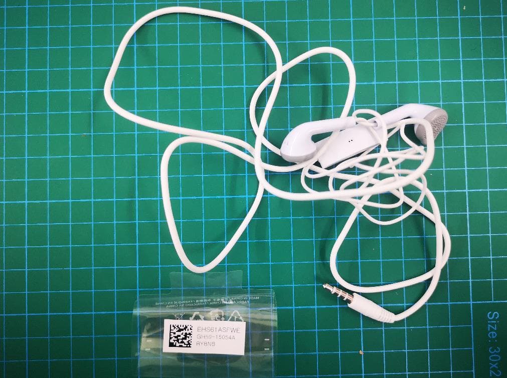
Click to zoom
Application Details
- Equipment Class
- PCE - PCS Licensed Transmitter held to ear
- Date of Grant
- May 16, 2021
- Application Purpose
- Original Equipment
- Date of Application
- May 05, 2021
- Equipment Note
- Multi-band GSM/WCDMA/LTE/5GNR Phone with Bluetooth,WLAN
- Frequency Range
- 834.00000000 - 839.00000000
- Country
- United States
Documents & Files
Document Text
Text extracted from the exhibit documents filed with the FCC. Open a document above to read the original.
Users Manual
Printed in Korea JM20-XXXX-XXXX Rev.1.0 English. 12/2020 QUICK START GUIDE !M"#$$% B 2 English ..........................................................................3 English 3 Package contents • Device • USB cable • Quick start guide • Ejection pin • USB power adaptor • The items supplied with the device and their images may vary by region. • Visit www.samsung.com to view device information, the user manual, and more. You may incur additional charges for accessing the Internet. Device layout To turn on the device, press and hold the Side key for a few seconds. Multipurpose jack (USB Type-C) Front camera SIM card / Memory card tray Side key Volume key EnglishQUICK START GUIDE 4 Rear camera The charger should remain close to the electric socket and easily accessible while charging. Installing a nano-SIM card Nano-SIM cards are sold separately. 231 Correct disposal This marking on the product, accessories or literature indicates that the product and its electronic accessories (e.g. charger, headset, USB cable) should not be disposed of with other household waste. This marking on the battery, manual or packaging indicates that the batteries in this product should not be disposed of with other household waste. Nano-SIM card English 5 Safety information Read all safety information before using the device to ensure safe and proper use. You can view more safety information in the safety information menu of the Settings app. Warning Follow the warnings below to prevent incidents, such as fires or explosions, injuries, or damage to the device • Do not expose the device to physical impact or damage. • Use only Samsung-approved batteries, chargers, and cables specifically designed for your device. • P revent the multipurpose jack and battery terminals from coming into contact with foreign materials such as metal, liquids, or dust. • If any part of the device, such as the glass or acrylic body, is broken, smokes, or emits a burning odor, stop using the device immediately. Use the device again only after it has been repaired at a Samsung Service Centre. • Do not turn on or use the device when the battery compartment is exposed. • Do not disassemble or reuse the battery. • Do not allow children or animals to chew or suck the device. • T he device can be used in locations with an ambient temperature of 0 °C to 35 °C. You can store the device at an ambient temperature of -20 °C to 50 °C. Using or storing the device outside of the recommended temperature ranges may damage the device or reduce the battery’s lifespan. • Do not use your device in a hot environment or near fire. • Comply with all safety warnings and regulations regarding mobile device usage while operating a vehicle. 6 Maximum SAR for this model and conditions under which it was recorded Head SAR Removing the battery • T o remove the battery, contact an authorised service centre. To obtain battery removal instructions, please visit www.samsung.com/global/ecodesign_energy. • For your safety, you must not attempt to remove the battery. If the battery is not properly removed, it may lead to damage to the battery and device, cause personal injury, and/or result in the device being unsafe. • Samsung does not accept liability for any damage or loss (whether in contract or tort, including negligence) which may arise from failure to precisely follow these warnings and instructions, other than death or personal injury caused by Samsung’s negligence. 0.77 W/kg Hot spot SAR 1.05 W/kg For SAR values for all other countries: For SAR values specific to your model, visit www.samsung.com/sar and search for your region and device with the model number. 0.79W/kg Body-worn SAR Body-worn SAR testing has been carried out at a separation distance of 1.5 cm. To meet RF exposure guidelines during body-worn operation, the device should be positioned at least this distance away from the body. Pursuant to Part 15.21 of the FCC Rules, you are cautioned that changes or modifications not expressly approved by Samsung could void your authority to operate the device. This device complies with Part 15 of the FCC Rules. Operation is subject to the following two conditions: (1) This device may not cause harmful interference, and (2) this device must accept any interference received, including interference that may cause undesired operation. Note: Any device that uses Bluetooth or Wi-Fi is subject to FCC Part 15. Any device with a power supply is subject to Part 15 which also covers both intentional radiators (Bluetooth and Wi-Fi) and unintentional radiators (such as emissions from power supplies and circuit boards). FCC Part 15 Information and Notices However, there is no guarantee that interference will not occur in a particular installation. If this equipment does cause harmful interference to radio or television reception, which can be determined by turning the equipment off and on, the user is encouraged to try to correct the interference by one or more of the following measures: • Reorient or relocate the receiving antenna. • Increase the separation between the equipment and receiver. • Connect the equipment into an outlet on a circuit different from that to which the receiver is connected. • Consult the dealer or an experienced radio/ TV technician for help. Responsible party - U.S. Contact Information Samsung Electronics America, Inc. QA Lab America 19 Chapin Rd. Building D, Pine Brook NJ 07058 Tel: 1-973-808-6375 Fax: 1-973-808-6361 Note: This equipment has been tested and found to comply with the limits for a Class B digital device, pursuant to Part 15 of the FCC Rules. These limits are designed to provide reasonable protection against harmful interference in a residential installation. This equipment generates, uses and can radiate radio frequency energy and, if not installed and used in accordance with the instructions, may cause harmful interference to radio communications. FCC Notice The device may cause TV or radio interference if used in close proximity to …
Text truncated - open the document above for the full version.
Users Manual
Printed in Korea JM20-XXXX-XXXX Rev.1.0 English. 12/2020 QUICK START GUIDE !M"#$$%B/DS 2 English ..........................................................................3 English 3 Package contents • Device • USB cable • Quick start guide • Ejection pin • USB power adaptor • The items supplied with the device and their images may vary by region. • Visit www.samsung.com to view device information, the user manual, and more. You may incur additional charges for accessing the Internet. Device layout To turn on the device, press and hold the Side key for a few seconds. Multipurpose jack (USB Type-C) Front camera SIM card / Memory card tray Side key Volume key EnglishQUICK START GUIDE 4 Rear camera The charger should remain close to the electric socket and easily accessible while charging. Installing a nano-SIM card Nano-SIM cards are sold separately. 231 Nano-SIM card 2 Nano-SIM card 1 Correct disposal This marking on the product, accessories or literature indicates that the product and its electronic accessories (e.g. charger, headset, USB cable) should not be disposed of with other household waste. This marking on the battery, manual or packaging indicates that the batteries in this product should not be disposed of with other household waste. English 5 Safety information Read all safety information before using the device to ensure safe and proper use. You can view more safety information in the safety information menu of the Settings app. Warning Follow the warnings below to prevent incidents, such as fires or explosions, injuries, or damage to the device • Do not expose the device to physical impact or damage. • Use only Samsung-approved batteries, chargers, and cables specifically designed for your device. • P revent the multipurpose jack and battery terminals from coming into contact with foreign materials such as metal, liquids, or dust. • If any part of the device, such as the glass or acrylic body, is broken, smokes, or emits a burning odor, stop using the device immediately. Use the device again only after it has been repaired at a Samsung Service Centre. • Do not turn on or use the device when the battery compartment is exposed. • Do not disassemble or reuse the battery. • Do not allow children or animals to chew or suck the device. • T he device can be used in locations with an ambient temperature of 0 °C to 35 °C. You can store the device at an ambient temperature of -20 °C to 50 °C. Using or storing the device outside of the recommended temperature ranges may damage the device or reduce the battery’s lifespan. • Do not use your device in a hot environment or near fire. • Comply with all safety warnings and regulations regarding mobile device usage while operating a vehicle. 6 Removing the battery • T o remove the battery, contact an authorised service centre. To obtain battery removal instructions, please visit www.samsung.com/global/ecodesign_energy. • For your safety, you must not attempt to remove the battery. If the battery is not properly removed, it may lead to damage to the battery and device, cause personal injury, and/or result in the device being unsafe. • Samsung does not accept liability for any damage or loss (whether in contract or tort, including negligence) which may arise from failure to precisely follow these warnings and instructions, other than death or personal injury caused by Samsung’s negligence. Maximum SAR for this model and conditions under which it was recorded Head SAR0.77 W/kg Hot spot SAR 1.05 W/kg For SAR values for all other countries: For SAR values specific to your model, visit www.samsung.com/sar and search for your region and device with the model number. 0.79 W/kg Body-worn SAR Body-worn SAR testing has been carried out at a separation distance of 1.5 cm. To meet RF exposure guidelines during body-worn operation, the device should be positioned at least this distance away from the body. Pursuant to Part 15.21 of the FCC Rules, you are cautioned that changes or modifications not expressly approved by Samsung could void your authority to operate the device. This device complies with Part 15 of the FCC Rules. Operation is subject to the following two conditions: (1) This device may not cause harmful interference, and (2) this device must accept any interference received, including interference that may cause undesired operation. Note: Any device that uses Bluetooth or Wi-Fi is subject to FCC Part 15. Any device with a power supply is subject to Part 15 which also covers both intentional radiators (Bluetooth and Wi-Fi) and unintentional radiators (such as emissions from power supplies and circuit boards). FCC Part 15 Information and Notices However, there is no guarantee that interference will not occur in a particular installation. If this equipment does cause harmful interference to radio or television reception, which can be determined by turning the equipment off and on, the user is encouraged to try to correct the interference by one or more of the following measures: • Reorient or relocate the receiving antenna. • Increase the separation between the equipment and receiver. • Connect the equipment into an outlet on a circuit different from that to which the receiver is connected. • Consult the dealer or an experienced radio/ TV technician for help. Responsible party - U.S. Contact Information Samsung Electronics America, Inc. QA Lab America 19 Chapin Rd. Building D, Pine Brook NJ 07058 Tel: 1-973-808-6375 Fax: 1-973-808-6361 Note: This equipment has been tested and found to comply with the limits for a Class B digital device, pursuant to Part 15 of the FCC Rules. These limits are designed to provide reasonable protection against harmful interference in a residential installation. This equipment generates, uses and can radiate radio frequency energy and, if not installed and used in accordance with the instructions, may cause harmful interference to radio communications. FCC Notice The device may cause TV or radio interference if used in…
Text truncated - open the document above for the full version.
Cover Letter(s)
Samsung Electronics Co., Ltd. 19 Chapin Rd.,Building D Pine Brook, NJ 07058 Tel: +1-201-937-4203 Authority to Act as Agent Date: __0415,2021_____ American Certification Body, Inc. 6731 Whittier Avenue Suite C110 McLean, VA 22101 To Whom It May Concern: __ ____(CTTL,Telecommunication Technology Labs,CAICT)______ is authorized to act on our behalf, until otherwise notified, for applications to American Certification Body, Inc. (ACB). We certify that we are not subject to denial of federal benefits, that includes FCC benefits, pursuant to Section 5301 of the Anti-Drug Abuse Act of 1988, 21 U.S.C. 862. Further, no party, as defined in 47 CFR 1.2002 (b) , to the application is subject to denial of federal benefits, that includes FCC benefits. Thank you, Agency Agreement Expiration Date: _____12 months_____ By: ____________ _____Jenni Chun_________ (Signature 1 ) (Print name) Title: ______Gene ral Manager________ On behalf of: __Samsung Electronics Co., Ltd. ___ (Compan y Name) Telephone: ___973-808-6375____ 022818 – 11 1 - Must be signed by applicant contact given for applicant on the FCC site, or by the authorized agent if an appropriate authorized agent letter has been provided. Letters should be placed on appropriate letterhead. Samsung Electronics Co., Ltd. 19 Chapin Rd.,Building D Pine Brook, NJ 07058 Tel: +1-201-937-4203 Request for Confidentiality Date: _0415,2021__ Subject: Confidentiality Request for: ____ZCASMA226B____ Pursuant to FCC 47 CFR 0.457(d) and 0.459 and IC RSP-100, Section 9.4, the applicant requests that a part of the subject FCC application be held confidential. Type of Confidentiality Requested Exhibit ☐Short Term☒Permanent Block Diagrams ☒Short Term External Photos ☒Short Term☐Permanent * 2 Internal Photos ☐Short Term☒Permanent Operation Description/Theory of Operation ☐Short Term☒Permanent Parts List & Placement/BOM ☐Short Term☒Permanent Tune-Up Procedure ☐Short Term☒Permanent Schematics ☒Short Term Test Setup Photos ☒Short Term☐Permanent * 3 User’s Manual _____SAMSUNG Electronics______ has spent substantial effort in developing this product and it is one of the first of its kind in industry. Having the subject information easily available to "competition" would negate the advantage they have achieved by developing this product. Not protecting the details of the design will result in financial hardship. Permanent Confidentiality: The applicant requests the exhibits listed above as permanently confidential be permanently withheld from public review due to materials that contain trade secrets and proprietary information not customarily released to the public. Short-Term Confidentiality: The applicant requests the exhibits selected above as short term confidential be withheld from public view for a period of __180___ days from the date of the Grant of Equipment Authorization and prior to marketing. This is to avoid premature release of sensitive information prior to marketing or release of the product to the public. Applicant is also aware that they are responsible to notify ACB in the event information regarding the product or the product is made available to the public before the requested period has expired. ACB will then release the The asterisked items (*) require further information to be provided to ACB before permanent confidentiality will be extended to these exhibits. Please refer to FCC KDB 726920 and the specific Document link for D01 found at: https://apps.fcc.gov/oetcf/kdb/forms/FTSSearchResultPage.cfm?switch=P&id=41731 and review section II, 3) regarding specific information that must accompany these requests. documents listed above for public disclosure pursuant to FCC Public Notice DA 04-1705. NOTE for Industry Canada Applications: regarding specific information that must accompany these requests. 022818 – 11 Samsung Electronics Co., Ltd. 19 Chapin Rd.,Building D Pine Brook, NJ 07058 Tel: +1-201-937-4203 IC currently only distinguishes Permanent Confidentiality exhibits as shown above. Short Term confidentiality is not considered applicable to IC applications. Sincerely, By: ______ /General Manager______ ___Jenni Chun____ (Signature/Title 3 ) (Print name) 3 - Must be signed by applicant contact given for applicant on the FCC site, or by the authorized agent if an appropriate authorized agent letter has been provided. Letters should be placed on appropriate letterhead. 022818 – 11
Cover Letter(s)
Statement We, __ Samsung Electronics Co., Ltd _____ declared that our device with FCC ID: ZCASMA226B, is a multi-band mobile phone which supports 2G : 850/ 900/ 1800/ 1900 3G : B1/ B2/ B5/ B8 LTE FDD : B1/ B2/ B3/ B5/ B7/ B8/ B20/ B28 LTE TDD : B38/ B40, B41(2496MHz~2690MHz. Full Band) 5G:n40; n78; ENDC: 7A_n5A However, LTE band 40、n40、n78 is not available in US market and Canada market, and will be disabled by software. Contact Person: Jenni Chun E-mail: [email protected]
Cover Letter(s)
PRODUCT EQUALITY DECLARATION We, Samsung Electronics Co., Ltd., declare that the “SM-A226B/DS” is the parent product of the “SM-A226B” And declare on our sole responsibility that the product (variant) SM-A226B HW version : REV1.0 SW version : A226B.001 is in all relevant parts identical to the product SM-A226B/DS HW version : REV1.0 SW version : A226B.001 The only difference between SM-A226B/DS and SM-A226B is: 1. H/W SM-A226B/DS GSM850/900/1800/1900;WCDMA B1/2/5/8;LTE B1/2/3/5/7/8/20/28/38/40/41 (2496MHz ~ 2690MHz. 194 Mhz);NR(NSA) n1/3/5/7/8/20/28/38/40/41/78/79 WIFI 2.4G 5G GPS BT . Without NFC Feature Dual SIM SM-A226B GSM850/900/1800/1900;WCDMA B1/2/5/8;LTE B1/2/3/5/7/8/20/28/38/40/41 (2496MHz ~ 2690MHz. 194 Mhz);NR(NSA) n1/3/5/7/8/20/28/38/40/41/78/79 WIFI 2.4G 5G GPS BT . Without NFC Feature Single SIM - PCB layout is same. -Antenna is the same. - The other parts are same. 2. S/W 1) Protocol is same. 2) Applications of MMS、RCS、IMS、SUPL, DM, FUMO feature is same. Author Information Signature Name Lizhonggang Place of Duty Protocol Certification part Tel +86-18321929116 E-mail [email protected]
External Photos
Sample01 Sample02 Sample03 Sample04 Sample05 Sample06 SIM tray 1:Dual SIM tray for SM-A226B/DS: Sim tray2: Single SIM tray for SM-A226B HS01: GH59-15054A 制造商 WATA HS02: GH59-15054A 制造商Yongbao Data Cable1:EP-DR140AWE(GH39-01999A/C) 制造商 RFTECH Data Cable2:EP-DR140AWE(GH39-01999A/C) 制造商 Ningbo Broad Telecommunication Co., Ltd Data Cable3:EP-DR140AWE(GH39-01999A/C) 制造商 DONGGUAN KSD CO.,LTD Data Cable4:EP-DR140AWE(GH39-01999A/C) 制造商 CRESYN HANOI Co.,Ltd CH01: R.F. Tech (EP-TA200) JBE OPEN CH02: Dongwon (EP-TA200) JBE CH03: SOLUM (EP-TA200) JWE/JBE
ID Label/Location Info
Label location SAMSUNG
Internal Photos
PCB 01: PCB 02: PCB 03: PCB 04: PCB 05: PCB 06: PCB 07: Battery:
RF Exposure Info
No.I21Z70041-SEM01 ©Copyright. All rights reserved by CTTL. Page 1 of 236 SAR TEST REPORT No. I21Z70041-SEM01 For SAMSUNG Electronics Co., Ltd. Multi-band GSM/WCDMA/LTE/5GNR Phone with Bluetooth,WLAN Model Name: SM-A226B/DS,SM-A226B with Hardware Version: REV1.0 Software Version: A226B.001 FCC ID: ZCASMA226B Issued Date: 2021-5-7 Note: The test results in this test report relate only to the devices specified in this report. This report shall not be reproduced except in full without the written approval of CTTL. The report must not be used by the client to claim product certification, approval, or endorsement by NVLAP, NIST, or any agency of the U.S.Government. Test Laboratory: CTTL, Telecommunication Technology Labs, CAICT No. 51, Xueyuan Road, Haidian District, Beijing, P. R. China 100191. Tel:+86(0)10-62304633-2512, Fax:+86(0)10-62304633-2504 Email: [email protected], website: www.caict.ac.cn No.I21Z70041-SEM01 ©Copyright. All rights reserved by CTTL. Page 2 of 236 REPORT HISTORY Report Number Revision Issue Date Description I21Z70041-SEM01 Rev.0 2021-4-15 Initial creation of test report I21Z70041-SEM01 Rev.1 2021-4-22 1.Revise Tx frequency of WiFi5G on section4.1 page9, and section11.4 page59-60. 2.Revise applicant information on section3.1. 3.Add some relative TCBC workshops for SAR measurement for EN-DC on section5.2. 4.Add power results of DL CA on page58. 5.Update the probe calibration report on ANNEX G. 6.Revise the simultaneous process of ENDC on Table13.4 page64. 7.Revise ENDC combination in SAR test setup photo. I21Z70041-SEM01 Rev.2 2021-4-29 1.Add SAR results for 10-g extremity SAR on section14.6. I21Z70041-SEM01 Rev.3 2021-5-1 Update the information on Table 2.3 page 7 and Table 13.2 page 64 of test report. I21Z70041-SEM01 Rev.4 2021-5-7 Update conductive power for DL CA on page58. No.I21Z70041-SEM01 ©Copyright. All rights reserved by CTTL. Page 3 of 236 TABLE OF CONTENT 1 TEST LABORATORY .................................................................................................................... 5 1.1 TESTING LOCATION ........................................................................................................................................ 5 1.2 TESTING ENVIRONMENT................................................................................................................................. 5 1.3 PROJECT DATA ............................................................................................................................................... 5 1.4 SIGNATURE ..................................................................................................................................................... 5 2 STATEMENT OF COMPLIANCE .................................................................................................. 6 3 CLIENT INFORMATION ................................................................................................................ 8 3.1 APPLICANT INFORMATION .............................................................................................................................. 8 3.2 MANUFACTURER INFORMATION ..................................................................................................................... 8 4 EQUIPMENT UNDER TEST (EUT) AND ANCILLARY EQUIPMENT (AE) ................................. 9 4.1 ABOUT EUT ................................................................................................................................................... 9 4.2 INTERNAL IDENTIFICATION OF EUT USED DURING THE TEST ........................................................................ 10 4.3 INTERNAL IDENTIFICATION OF AE USED DURING THE TEST .......................................................................... 10 5 TEST METHODOLOGY .............................................................................................................. 11 5.1 APPLICABLE LIMIT REGULATIONS ................................................................................................................ 11 5.2 APPLICABLE MEASUREMENT STANDARDS ................................................................................................... 11 6 SPECIFIC ABSORPTION RATE (SAR) ...................................................................................... 12 6.1 INTRODUCTION ............................................................................................................................................. 12 6.2 SAR DEFINITION .......................................................................................................................................... 12 7 TISSUE SIMULATING LIQUIDS ................................................................................................. 13 7.1 TARGETS FOR TISSUE SIMULATING LIQUID .................................................................................................... 13 7.2 DIELECTRIC PERFORMANCE ......................................................................................................................... 13 8 SYSTEM VERIFICATION ............................................................................................................ 17 8.1 SYSTEM SETUP ............................................................................................................................................. 17 8.2 SYSTEM VERIFICATION ................................................................................................................................. 18 9 MEASUREMENT PROCEDURES .............................................................................................. 19 9.1 TESTS TO BE PERFORMED ............................................................................................................................. 19 9.2 GENERAL MEASUREMENT PROCEDURE ........................................................................................................ 21 9.3 WCDMA MEASUREMENT PROCEDURES FO…
Text truncated - open the document above for the full version.
RF Exposure Info
No.I21Z70041-SEM01 ©Copyright. All rights reserved by CTTL. Page 157 of 236 No.I21Z70041-SEM01 ©Copyright. All rights reserved by CTTL. Page 158 of 236 No.I21Z70041-SEM01 ©Copyright. All rights reserved by CTTL. Page 159 of 236 No.I21Z70041-SEM01 ©Copyright. All rights reserved by CTTL. Page 160 of 236 No.I21Z70041-SEM01 ©Copyright. All rights reserved by CTTL. Page 161 of 236 No.I21Z70041-SEM01 ©Copyright. All rights reserved by CTTL. Page 162 of 236 No.I21Z70041-SEM01 ©Copyright. All rights reserved by CTTL. Page 163 of 236 No.I21Z70041-SEM01 ©Copyright. All rights reserved by CTTL. Page 164 of 236 No.I21Z70041-SEM01 ©Copyright. All rights reserved by CTTL. Page 165 of 236 No.I21Z70041-SEM01 ©Copyright. All rights reserved by CTTL. Page 166 of 236 No.I21Z70041-SEM01 ©Copyright. All rights reserved by CTTL. Page 167 of 236 No.I21Z70041-SEM01 ©Copyright. All rights reserved by CTTL. Page 168 of 236
RF Exposure Info
No.I21Z70041-SEM01 ©Copyright. All rights reserved by CTTL. Page 169 of 236 No.I21Z70041-SEM01 ©Copyright. All rights reserved by CTTL. Page 170 of 236 No.I21Z70041-SEM01 ©Copyright. All rights reserved by CTTL. Page 171 of 236 No.I21Z70041-SEM01 ©Copyright. All rights reserved by CTTL. Page 172 of 236 No.I21Z70041-SEM01 ©Copyright. All rights reserved by CTTL. Page 173 of 236 No.I21Z70041-SEM01 ©Copyright. All rights reserved by CTTL. Page 174 of 236 No.I21Z70041-SEM01 ©Copyright. All rights reserved by CTTL. Page 175 of 236 ANNEX H Dipole Calibration Certificate 835 MHz Dipole Calibration Certificate No.I21Z70041-SEM01 ©Copyright. All rights reserved by CTTL. Page 176 of 236 No.I21Z70041-SEM01 ©Copyright. All rights reserved by CTTL. Page 177 of 236 No.I21Z70041-SEM01 ©Copyright. All rights reserved by CTTL. Page 178 of 236 No.I21Z70041-SEM01 ©Copyright. All rights reserved by CTTL. Page 179 of 236 No.I21Z70041-SEM01 ©Copyright. All rights reserved by CTTL. Page 180 of 236 No.I21Z70041-SEM01 ©Copyright. All rights reserved by CTTL. Page 181 of 236 No.I21Z70041-SEM01 ©Copyright. All rights reserved by CTTL. Page 182 of 236
RF Exposure Info
No.I21Z70041-SEM01 ©Copyright. All rights reserved by CTTL. Page 183 of 236 1900 MHz Dipole Calibration Certificate No.I21Z70041-SEM01 ©Copyright. All rights reserved by CTTL. Page 184 of 236 No.I21Z70041-SEM01 ©Copyright. All rights reserved by CTTL. Page 185 of 236 No.I21Z70041-SEM01 ©Copyright. All rights reserved by CTTL. Page 186 of 236 No.I21Z70041-SEM01 ©Copyright. All rights reserved by CTTL. Page 187 of 236 No.I21Z70041-SEM01 ©Copyright. All rights reserved by CTTL. Page 188 of 236 No.I21Z70041-SEM01 ©Copyright. All rights reserved by CTTL. Page 189 of 236 No.I21Z70041-SEM01 ©Copyright. All rights reserved by CTTL. Page 190 of 236 No.I21Z70041-SEM01 ©Copyright. All rights reserved by CTTL. Page 191 of 236 2450 MHz Dipole Calibration Certificate No.I21Z70041-SEM01 ©Copyright. All rights reserved by CTTL. Page 192 of 236 No.I21Z70041-SEM01 ©Copyright. All rights reserved by CTTL. Page 193 of 236 No.I21Z70041-SEM01 ©Copyright. All rights reserved by CTTL. Page 194 of 236 No.I21Z70041-SEM01 ©Copyright. All rights reserved by CTTL. Page 195 of 236 No.I21Z70041-SEM01 ©Copyright. All rights reserved by CTTL. Page 196 of 236 No.I21Z70041-SEM01 ©Copyright. All rights reserved by CTTL. Page 197 of 236 No.I21Z70041-SEM01 ©Copyright. All rights reserved by CTTL. Page 198 of 236 No.I21Z70041-SEM01 ©Copyright. All rights reserved by CTTL. Page 199 of 236 2600 MHz Dipole Calibration Certificate No.I21Z70041-SEM01 ©Copyright. All rights reserved by CTTL. Page 200 of 236 No.I21Z70041-SEM01 ©Copyright. All rights reserved by CTTL. Page 201 of 236 No.I21Z70041-SEM01 ©Copyright. All rights reserved by CTTL. Page 202 of 236 No.I21Z70041-SEM01 ©Copyright. All rights reserved by CTTL. Page 203 of 236 No.I21Z70041-SEM01 ©Copyright. All rights reserved by CTTL. Page 204 of 236 No.I21Z70041-SEM01 ©Copyright. All rights reserved by CTTL. Page 205 of 236 No.I21Z70041-SEM01 ©Copyright. All rights reserved by CTTL. Page 206 of 236 No.I21Z70041-SEM01 ©Copyright. All rights reserved by CTTL. Page 207 of 236 5G Dipole Calibration Certificate No.I21Z70041-SEM01 ©Copyright. All rights reserved by CTTL. Page 208 of 236 No.I21Z70041-SEM01 ©Copyright. All rights reserved by CTTL. Page 209 of 236 No.I21Z70041-SEM01 ©Copyright. All rights reserved by CTTL. Page 210 of 236
RF Exposure Info
No.I21Z70041-SEM01 ©Copyright. All rights reserved by CTTL. Page 211 of 236 No.I21Z70041-SEM01 ©Copyright. All rights reserved by CTTL. Page 212 of 236 No.I21Z70041-SEM01 ©Copyright. All rights reserved by CTTL. Page 213 of 236 No.I21Z70041-SEM01 ©Copyright. All rights reserved by CTTL. Page 214 of 236 No.I21Z70041-SEM01 ©Copyright. All rights reserved by CTTL. Page 215 of 236 No.I21Z70041-SEM01 ©Copyright. All rights reserved by CTTL. Page 216 of 236 No.I21Z70041-SEM01 ©Copyright. All rights reserved by CTTL. Page 217 of 236 No.I21Z70041-SEM01 ©Copyright. All rights reserved by CTTL. Page 218 of 236 No.I21Z70041-SEM01 ©Copyright. All rights reserved by CTTL. Page 219 of 236 No.I21Z70041-SEM01 ©Copyright. All rights reserved by CTTL. Page 220 of 236 No.I21Z70041-SEM01 ©Copyright. All rights reserved by CTTL. Page 221 of 236 No.I21Z70041-SEM01 ©Copyright. All rights reserved by CTTL. Page 222 of 236 No.I21Z70041-SEM01 ©Copyright. All rights reserved by CTTL. Page 223 of 236 No.I21Z70041-SEM01 ©Copyright. All rights reserv…
Text truncated - open the document above for the full version.
Contact Information
Applicant
Jenni Chun(Senior Engineer)
Technical Contact
CTTL-Terminals Test Lab of China Academy of TelecoYin Feng
[email protected]86-10-62304633
No. 52, Huayuan Bei Road, Haidian District, · China
Test Firm
Telecommunication Technology Labs, CAICTYaqin Shen
Technical Specifications
| # | Rule Parts | Frequency Range | Power Output | Emission | Tolerance |
|---|---|---|---|---|---|
| 24 | 22H | 834 MHz - 839 MHz | 24.00 mW | 18M1G7D | 0.1 ppm |
Other Applications from SAMSUNG Electronics Co., Ltd.
ZCASMR391
Aug 04, 2026Wearable Device
Equipment Class
JBP - Part 15 Class B Computing Device PeripheralZCASMA085M
Jul 10, 2026Multi-band GSM/WCDMA/LTE Mobile Phone with Bluetooth, WLAN
Equipment Class
JBP - Part 15 Class B Computing Device PeripheralZCASMA076M
Nov 26, 2025Multi-band GSM/WCDMA/LTE/5GNR Mobile Phone with Bluetooth,WLAN
Equipment Class
JBP - Part 15 Class B Computing Device PeripheralZCASMA065M
Jul 03, 2024Multi-band GSM/WCDMA/LTE Mobile Phone with Bluetooth,WLAN
Equipment Class
CXX - Communications Rcvr for use w/ licensed Tx and CBsZCASMA065F
Jun 30, 2024Multi-band GSM/WCDMA/LTE Phone with Bluetooth,WLAN
Equipment Class
DSS - Part 15 Spread Spectrum Transmitter