ZFT-K105MOBILE PHONE-GSM PORTION
Global Mobile Communication (HK) Ltd.
Click to zoom
Application Details
- Equipment Class
- PCE - PCS Licensed Transmitter held to ear
- Date of Grant
- Apr 24, 2011
- Application Purpose
- Original Equipment
- Date of Application
- Apr 24, 2011
- Equipment Note
- MOBILE PHONE-GSM PORTION
- Frequency Range
- 1850.20000000 - 1909.80000000
- Country
- Hong Kong
Documents & Files
Document Text
Text extracted from the exhibit documents filed with the FCC. Open a document above to read the original.
Users Manual
-1- User Manual -2- WELCOME! PLEASE READ THIS INFORMATION BEFORE USING THE PHONE. B-MOBILE® IS NOT RESPONSIBLE FOR ANY DAMAGE/S DUE TO MISINTERPRETATION OF THIS INFORMATION AND MISUSE OF PRODUCT. B-MOBILE™ aims to improve its products and services and reserves all rights to revise/change the description of this product and its software as well as this user’s manual without obligation to notify any person of such revisions and changes. Some features introduced in this manual are network or subscription-dependent features. Please contact your service provider for more information. -3- 1 General Information 1.1 Profile Please read this pamphlet carefully in order to make your phone in perfect condition. Perfectly combining humanized design and fine art, this mobile phone provides a streamlined outlook, comfortable hand-feeling, pleasant sounds and MP3 player which bring convenience and fun to your work. Our company may change this mobile phone without prior written notice and reserves the final right to interpret the performance of this mobile phone. Due to different software and network operators, display on your phone may be different, refer to your phone for details. 1.2 Safety Information If your phone has lost or been stolen, notify the telecommunication office the SIM card is disabled (network support is required). This can avoid economic loss caused by unauthorized use. Please take measures as following to avoid your phone being unauthorized use: · Set PIN code of SIM card · Set phone password -4- 1.3 Safety warning and Attentions Safety warning Ø ROAD SAFETY COMES FIRST Do not use a hand-held phone while driving. Use hands-free fittings when calls are unavoidable while driving. In some countries, dialing or receiving calls while driving is illegal! Ø SWITCH OFF IN AIRCRAFT Wireless devices can cause interference in aircraft. Using a mobile phone in flight is illegal and risky. Please make sure that your mobile phone is powered off in flight. Ø SWITCH OFF BEFORE ENTERING RISKY AREAS Strictly observe the relevant laws, codes, and regulations on the use of mobile phones in risky areas. Turn off your mobile phone before entering a place susceptible to explosion, such as an oil station, oil tank, chemical plant or a place where a blasting process is under way. Ø OBSERVE ALL SPECIAL REGULATIONS Follow any special regulations in force in any area such as hospitals and always switch off your phone whenever it is forbidden to use it or, when it may cause interference or danger. Properly use your mobile phone near medical apparatuses, such as pacemakers, hearing aids and some other electronic medical devices, as it may cause interference to such apparatuses. Ø INTERFERENCE The conversation quality of any mobile phone may be affected by radio interference. An antenna is built inside the mobile phone and located below the microphone. Do not touch the antenna area during a conversation, lest that the conversation quality deteriorate. -5- Ø QUALIFIED SERVICE Only qualified personnel may install or repair phone equipment. Installing or repairing the mobile phone on your own may bring great danger and violates the warranty rules. Ø ACCESSORIES AND BATTERIES Use only approved accessories and batteries. Ø USE SENSIBLY Use only in a normal and proper manner. Ø EMERGENCY CALLS Ensure the phone is switched on and in service, enter the emergency number, e.g. 112, then press the Dial key. Give your location and state your situation briefly. Do not end the call until told to do so. Note: Just like all other mobile phones, this mobile phone does not necessarily support all the features described in this manual due to network or radio transmission problems. Some networks even do not support the emergency call service. Therefore, do not rely solely on the mobile phone for critical communications such as first aid. Please consult the local network operator. Precautions This mobile phone is well designed with fine art. Please exercise special care when using it. The following suggestions will help your mobile phone survive the warranty period and extend its service life: Ø Keep the mobile phone and all its fittings beyond children's reach. Ø Keep the mobile phone dry. Keep away from rain, moisture, liquid or other substances that may corrode electronic circuits. -6- Ø Do not use or store the mobile phone in dusty places, lest that active parts of the mobile phone be damaged. Ø Do not store the mobile phone in a high-temperature place. High temperature will shorten the life of electronic circuits and damage the battery and some plastic parts. Ø Do not store the mobile phone in a chilly place. Otherwise, moistures will be formed inside the mobile phone to damage electronic circuits when the mobile phone is moved to a constant temperature place. Ø Do not throw, knock or shock the mobile phone, as that will destroy the internal circuits and high-precision components of the mobile phone. 2 Your phone 2.1 Phone overview 2.2 Functions of Keys The mobile phone provides the following keys: u Left and right soft key The bottom line on the screen displays the functions of the Left and Right soft key. u SIM1 dial key(use same key with Left soft key) Press it to originate a call on SIM card 1 by entering the called number or selecting a contact from the phonebook; or press it to receive an incoming call; or press it in standby state to show the latest call records u SIM2 dial key -7- Press it to originate a call on SIM card 1 by entering the called number or selecting a contact from the phonebook; or press it to receive an incoming call; or press it in standby state to show the latest call records. u End key Press it to end a call being dialed or end an ongoing call; or press it to exit the menu and return to the standby state; or hold it for two or three seconds to power on or off the mobile phone. u Direction key Press them to scroll the options when browsing a function list. In edit state, press direc…
Text truncated - open the document above for the full version.
Cover Letter(s)
Global Mobile Communication (HK) ltd., FCC ID: ZFT-K105 POWER OF ATTORNEY April 18, 2011 Federal Communications Commission Authorization and Evaluation Division 7435 Oakland Mills Road Columbia, MD 21046 To Whom It May Concern: We, Global Mobile Communication (HK) ltd.,hereby authorize Shenzhen Super Test Service Technology Co., Ltd. (Terry YANG/ Manager) located at No.5, Langshan 2nd Rd., North Hi-Tech Industrial Park ,Nanshan, Shenzhen, Guangdong ,China on our behalf, to apply to the Federal Communications Commission on our equipment. Any and all acts carried out by Shenzhen Super Test Service Technology Co., Ltd. (Terry YANG/ Manager) on our behalf shall have the same effect as acts of our own. This authorization expires on May 31, 2011. This is to advise that we are in full compliance with the Anti-Drug Abuse Act. We, Global Mobile Communication (HK) ltd.,are not subject to a denial of federal benefits pursuant to Section 5301 of the Anti-Drug Act of 1988, 21 USC853a, and no party to the application is subject to a denial of federal benefits pursuant to that section. ChunLu Guo Sales Global Mobile Communication (HK) ltd., April 18, 2011
External Photos
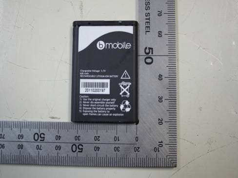
Report No: KS110407B01 Date of Issue: April 18, 2011 FCC ID: ZFT-K105 EXTERNAL PHOTOGRAPHS OF EUT Report No: KS110407B01 Date of Issue: April 18, 2011 FCC ID: ZFT-K105 Report No: KS110407B01 Date of Issue: April 18, 2011 FCC ID: ZFT-K105 Report No: KS110407B01 Date of Issue: April 18, 2011 FCC ID: ZFT-K105 Report No: KS110407B01 Date of Issue: April 18, 2011 FCC ID: ZFT-K105 Report No: KS110407B01 Date of Issue: April 18, 2011 FCC ID: ZFT-K105
Internal Photos
Report No: KS110407B01 Date of Issue: April 18, 2011 FCC ID: ZFT-K105 INTERNAL PHOTOGRAPHS OF EUT Report No: KS110407B01 Date of Issue: April 18, 2011 FCC ID: ZFT-K105 Report No: KS110407B01 Date of Issue: April 18, 2011 FCC ID: ZFT-K105 GSM antenna Report No: KS110407B01 Date of Issue: April 18, 2011 FCC ID: ZFT-K105 Bluetooth antenna Report No: KS110407B01 Date of Issue: April 18, 2011 FCC ID: ZFT-K105 Report No: KS110407B01 Date of Issue: April 18, 2011 FCC ID: ZFT-K105
Operational Description
1/2 Operation Description OPERATIONAL DESCRIPTION APPLICANT: Global Mobile Communication (HK) ltd., Manufacturer: Water World Technology Co., ltd FCC ID:ZFT-K107 Instruction Book: Users Manual Frequency Range GSM Transmit Frequency Band: 824.2-848.8 MHz Receive Frequency Band: 849.2-893.8 MHz Transmit Frequency Band: 1850.2-1909.8 MHz Receive Frequency Band: 1930.2-1989.8 MHz Specific Operating Power Range: Power Class 1; Power Control Level 0 +30dBm +2.0dB/-2.0dB Power Control Level 1 +28dBm +3.0dB/-3.0dB Power Control Level 2 +26dBm +3.0dB/-3.0dB Power Control Level 3 +24dBm +3.0dB/-3.0dB Power Control Level 4 +22dBm +3.0dB/-3.0dB Power Control Level 5 +20dBm +3.0dB/-3.0dB Power Control Level 6 +18dBm +3.0dB/-3.0dB Power Control Level 7 +16dBm +3.0dB/-3.0dB Power Control Level 8 +14dBm +3.0dB/-3.0dB Power Control Level 9 +12dBm +4.0dB/-4.0dB Power Control Level 10 +10dBm +4.0dB/-4.0dB Power Control Level 11 +8dBm +4.0dB/-4.0dB Power Control Level 12 +6dBm +4.0dB/-4.0dB Power Control Level 13 +4dBm +4.0dB/-4.0dB Power Control Level 14 +2dBm +5.0dB/-5.0dB Power Control Level 15 +0dBm +5.0dB/-5.0dB Note; Effective radiation efficiency is –3.7dB DC Voltage and Current into the Final Amplifier Module: Supply Voltage = 5.0Vdc Supply Current = ~0.5Amp. Tune-up Procedure: Tune-up Procedure Equipment Identification: Equipment's Identification label and its intended Location are as shown in EXHIBIT Type “ID Label / Location Information” (FCC ID Nameplate), and in EXHIBIT Type “Internal Photo”(Photograph of inside) Photographs: A complete set of the Photographs showing External and Internal Views of Circuit Details and Construction are provided by from EXHIBIT Type “External Photos” and “Internal Photos”. Accessories: Accessories 2/2 Operation Description Figure 1.2: Terminal Components (Accessories) Technical Descriptions TX synthesizer uses an Offset-PLL circuit. The Offset-PLL circuit consists of PLL-IC and TX_VCO and loop filter. Reference frequency of the above synthesizers is 26MHz and generated by VCTCXO. Control signal is sent from Baseband section and keeps frequency stability. TX IQ signal is input from Baseband section to MT6235, The Bluetooth signal is input form MT6601 and FM signal is input form TLG1120 section to MT6235. TX IQ signal is applied to the quadrature up-converter, and the up-converter LO signal is generated from the transceiver VCO within MT6139B. This up-converter translates the GMSK-modulated signal to an intermediate frequency (IF) that forms one input to a frequency/phase detector circuit. This IF signal is the reference input to an Offset-PLL circuit. The feedback path of this Offset-PLL circuit includes a down-conversion from the RF output frequency range to the IF range. The two inputs to this down-conversion mixer are formed the TX_VCO output and the LO generation circuits. The mixer output is the offset feedback signal that forms the variable input to a frequency/phase detector circuit. The detector compares its variable input to its reference input and generates an error signal that is low-pass filtered by the loop filter and applied to TX_VCO to force the RF frequency in the direction that minimizes errors. The TX_VCO output passes PA, Antenna SW, Coaxial connector with switch and emitted from embedded antenna. Digital Modulation: Analog speech produced by a microphone is encoded to digital PCM samples using a CODEC. The PCM samples are passed to a Vocoder for AMR (Advanced Multi Rate) encoding, to compress the speech samples. The encoding rate is determined by the Vocoder which formats the speech samples as data packets. A new data packet with data rate information is read by the microprocessor every 20 ms. The speech CODEC becomes AMR, FR(Full Rate), EFR(Enhanced FR) and HR(Half Rate). The microprocessor then sends the data packet to the transmit subsystem, and passed DAC to covert analog signal. I/Q base band signal is filtered and is inputted into 6M4003 containing quadrature phase modulator. Battery AC Charger
Parts List/Tune Up Info
NO.1 Comment describing Footprint Designator dosage Part NO. R 1 0R 电阻,0 ohm,±5%,1/16W,0402 0402 L301,LZ7,LZ201-LZ202,R10,R44,R47,R4,R503-R504,R512,R522,R800-R801,R411,LZ6,LZ8,C22,L303(校准 后删除) 19 RC0402JR-070R(LF) 2 0R 电阻,0 ohm,±5%,1/10W,0603 0603 R35,R23( 校准后焊接) 2 RC0603JR-070R(LF) 3 0.36 电阻,0.36 ohm,±1%,1/4W,0805 0402 R300 1 RL0805FR-7W0R36(LF) 5 15R 电阻,15 ohm,±5%,1/16W,0402 0402 R22 1 RC0402JR-0715R(LF) 6 18R 电阻,18 ohm,±5%,1/10W,0603 0402 R406 1 RC0402JR-0718R(LF) 7 33R 电阻,33 ohm,±5%,1/16W,0402 0402 R11,R26,R13,R17,R64-R65,R7,R202 8 RC0402JR-0733R(LF) 8 100R 电阻,100 ohm,±5%,1/16W,0402 0402 R205,R208,R440-R441 4 RC0402JR-07100R(LF) 9 510R 电阻,510 ohm,±5%,1/16W,0402 0402 R200,R209 2 RC0402JR-07510R(LF) 10 1K 电阻,1K ohm,±5%,1/16W,0402 0402 R2,R8,R204,R3,R15,R24,R231,R405,R407-R408 10 RC0402JR-071K(LF) 12 2K 电阻 2 K ohm ±5% 1/16W 0402 0402 R206 1 RC0402JR-072K(LF) 12 2K 电阻 , 2 K o h m, ±5% , 1/16W , 0402 0402 R206 1 14 10K 电阻,10K ohm,±5%,1/16W,0402 0402 R34,R16,R511,R513 4 RC0402JR-0710K(LF) 15 15K 电阻,15K ohm,±5%,1/16W,0402 0402 R401 1 RC0402JR-0715K(LF) 16 20K 电阻 20K ohm,±5%,1/16W,0402 0402 R213 1 RC0402JR-0720K(LF) 17 47K 电阻,47K ohm,±5%,1/16W,0402 0402 R5,R20 2 RC0402JR-0747K(LF) 18 100K 电阻 ,100K ohm,±5%,1/16W,0402 0402 R214-R215,R6 3 RC0402JR-07100K(LF) 19 150K 电阻 ,150K ohm,±5%,1/16W,0402 0402 R36 1 RC0402JR-07150K(LF) C 22 1.5pF 电容 ,1.5pF,±0.25pF,50V,COG,0402 0402 C414-C415 2 GRM1555C1H1R5CZO1D 23 2.2pF 电容 ,2.2pF,±0.25pF,50V,COG,0402 0402 C404-C405 2 GRM1555C1H2R2CZO1D 24 3.3pF 电容 ,3.3pF,±0.25pF,50V,COG,0402 0402 C425-C426,C428-C429 4 GRM1555C1H3R3CZO1D 25 4.7pF 电容 ,4.7pF,±0.25pF,50V,COG,0402 0402 C418 1 GRM1555C1H4R7CZO1DGRM1555C1H100JZ0 26 10pF 电容 ,10pF,±5%,50V,COG,0402 0402 C401 1 GRM1555C1H100JZ01D 27 18pF 电容 ,18pF,±5%,50V,COG,0402 0402 C251-C252,C411,ED3-ED6,ED400-ED403,ED201,ED203 13 GRM1555C1H180JZ01D 28 22pF 电容 ,22pF,±5%,50V,COG,0402 0402 C7,C203,C456 3 GRM1555C1H220JZ01D 30 27pF 电容 ,27pF,±5%,50V,COG,0402 0402 C431,C23 2 GRM1555C1H270JZ01D 31 33pF 电容 ,33pF,±5%,50V,COG,0402 0402 C3-C4,C14,C19-C21,C26,C28-C29,C31-C33,C36,C47-C50,C205,C208-C210,C216,C410,ED213-ED214,ED220- ED221,VR2 28 GRM1555C1H330JZ01D 32 47pF 电容 ,47pF,±5%,50V,COG,0402 0402 C435 1 GRM1555C1H470JZ01D 33 56pF 电容 ,56pF,±5%,50V,COG,0402 0402 C455 1 GRM1555C1H560JZ01D 34 100pF 电容 ,100pF,±5%,50V,COG,0402 0402 C250,C13,C15,C219,C406-C407,C409,C413 8 GRM1555C1H101JD01D(LF) 35 470pF 电容 ,470pF,±10%,50V,X7R,0402 0402 C44 1 GRM1555C1H471JZ01D 36 680pF 电容 ,680pF,±10%,50V,COG,0402 0402 C402-C403 2 GRM1555C1H681JZ01D 37 1nF 电容,1nF,±10%,50V,X7R,0402 0402 C45 1 GRM155R71H102KA01D(LF) 38 10nF 电容 ,10nF,±10%,16V,X7R,0402 0402 C38,C300,C436 3 GRM155R71C103KA01D(LF) 39 22nF 电容 ,22nF,±10%,16V,X7R,0402 0402 C204,C212,C221 3 GRM155R71C223KA01D(LF) 40 100nF 电容 ,100nF,±10%,10V,X5R,0402 0402 C802-C803,C39,C10,C35,C200,C206,C217,C8,C61,C400,C501,C6 00,C800 - C801,C502 16 GRM155R71C104KA88D(LF) 41 1uF 电容,1uF,±10%,10V,X5R,0603 0603 C5,C58-C59 3 GRM188R61A105KA61D(LF) 42 1uF 电容,1uF,±10%,6.3V,X5R,0402 0402 C1,C6,C24,C27,C37,C56,C2,C17,C46,C51,C420-C423 14 GRM155R60J105KE19D(LF) 43 2.2uF 电容,2.2uF,±10%,6.3V,X5R,0603 0603 C218,C9,C60,C202,C304-C305,C308-C310 9 GRM188R60J225KE19D 44 4.7uF 电容,4.7uF,±10%,6.3V,X5R,0603 0603 C57 1 GRM188R60J475KE19D 45 10uF 电容,10uF,±20%,6.3V,X5R,0805 0805 C11,C201,C213,C211,C303,C437,C624 7 JMK212BJ106KG-T L 46 2.4nH 电感,2.4nH,±0.3nH , 0402 , SDCL1005C2N4STDF , SUNLORD 0402 L404 1 SDCL1005C2N4ST 48 6.2nH 电感 ,6.2nH,±0.3nH,0402,SDCL1005C6N2STDF, S 0402 L405-L406 2 SDCL1005C6N2ST 49 10nH 电感 ,10nH,±5%,0402,SDCL1005C10NJTDF,Sunl o 0402 L400 1 SDCL1005C10NJT 50 15nH 电感 ,15nH,±5%,0402,SDCL1005C15NJTDF,Sunl o 0402 L403 1 SDCL1005C15NJT 51 100nH 电感,100nH,±5%,0402,SDCL1005CR10JTDF,Sun l 0402 L1 1 SDCL1005C100NJT 49 0402 磁珠 ,75 ohm,0402,SZ1005G750TF,Sunlord 0402 LZ1-LZ2,LZ207-LZ20 84 SZ1005G750TF 51 HZ1005K182TF 磁珠,1.8Kohm , 50mA , 0402 , HZ1005K182TF , SUNLORD 0402 LZ3-LZ5,R210-R212,L800 6 HZ1005K182TF 52 DIODE 肖特基二极管 ,SIG631E30T1G,SOD-523,SIG SOD-523 D413 1 SIG631E30T1G 53 PNP P-FET;0.28ohm;-0.86A;0.29W;SC-70-3 , SI1305DL-T1-E3 , VISHAY SC-70 Q1 1 SI1305DL-T1-E3 55 TPCF8B01 场效应管 ,TPCF8B01,TOSHIBA 场效应管 , T Q301 1 TPCF8B01 57 LED 0603 LED(蓝),BL-HB336G-TRB,BRIGHT 0603 LD1,LD4-LD5,LD34 4 BL-HB336G-TRB 58 NPN 三极管 ,DTC114TKA,SC-59,ROHM SC-59 Q5 1 DTC114TKA 59 TVS TVS二极管,(5V,80pf),ESD5Z5.0T1G,SOD523,ON S SOD523 TVS301 1 ESD5Z5.0T1G 60 CPU SC6600L2 BGA-224 U100 1 SC6600L2 61 RF PA 四频发射模块 (EGSM),AM7803,AMALFI 22 PAD U402 1 AM7803 62 RF TRANSCEIVER QS518,TRANSCEIVER QFN-40 U404 1 QS518 TRANSCEIVER 63 SAW 双路滤波器 (DCS/EGSM),SFR942PY002,WISOL 10 PAD U405 1 SFR942PY002 66 MEMORY MCP,PSRAM+NOR FLASH(32Mb+16Mb),EN71GL032A0 FBGA-56 U501 1 EN71GL032A0-70CWP 67 AUDIO PA 音频功放 ,SN4990AIF09E,SI-EN CSP-9 U201 1 SN4990AIF09E 68 BT 蓝牙芯片 ,6x6mm,40Pin QFN,RDA5870E,RDA QFN-40 U1 1 RDA5870E 69 CONNECTOR 电池连接器,普通,3.0PITCH,8.4x3.5x6.2mmH,WKBAV006-D31P,杰顺通 8.4x3.5x6.2mmH U9 1 WKBAV006-D31P 70 SIM SOCKET SIM卡连接器, 普通型,1.80mmH,SIMMS-00615- TP31(CAF99-06183-1503) , LCN 3PIN SIM1,SIM400 2 CAF99-06183-1503 71 T-FLASHSOCKET T-FLASH卡座,掀盖型,1.9mmH,CAH11-08193-SF01 , LCN 8PIN TF100 1 CAH11-08193-SF01 72 USB SOCKET MINI USB插座,12PIN,2.0mmH,MICFS-01215-TP03(UAF05-12204-1501) , LCN 12PIN USB400 1 UAF05-12204-1501 73 CRYSTAL 32.768KHz晶体,12.5pF,±20ppm,Q13MC1462000200(Q13MC1461000200),EPSON 4 PAD X200 1 Q13MC1462000200 74 CRYSTAL 26MHz晶体(3225),±10ppm,8.0pf,TN4- 26245 EPSON 3225 X400 1 TN4-26245 26245,EPSON 75 PCB PCB主板,7707-MB-V1.3 91.6mmX36mmX1mm 1
Parts List/Tune Up Info
PDF 文件使用 "pdfFactory Pro" 试用版本创建 www.fineprint.cn PDF 文件使用 "pdfFactory Pro" 试用版本创建 www.fineprint.cn
Parts List/Tune Up Info
Tune UP 1 Adjustment of RF Output Power: (1) The equipment setup as shown in Figure 1. (2) Operation of PC adjusts equipment. (3) Use RF Engineering Tools at PC side. Select GSM850 Band: 1) Set GSM850 Band. 2) Set ARFCN: 190 3) TX ON. 4) Adjust the power to 32.4dBm (Power control level: PCL=5) by PA DAC value. 5) Repeat 4) for 15 times,and adjust the power level to 30.5, 28.8, 27, 25, 23, 21, 19, 17, 15, 13, 11, 9, 7, 5. 6) Make 16 Ramp-Up/Ramp-Down data from the adjustment value of (5) and (6). PC RF Tester GPIB Cable UART Cable RF Cable Test sample Figure 1 7) Data of 5) and 6) is writen to flash memory. Select PCS1900 Band: 1) Set PCS Band. 2) Set ARFCN: 661. 3) TX ON. 4) Adjust the power to 29.0 dBm (Power control level: PCL=0) by PA DAC value. 5) Repeat 4) for 15 times,and adjust the power level to 27.5, 26, 24, 22, 20, 18, 16, 14, 12, 10, 8, 6, 4, 2, 0. 6) Make 16 Ramp-Up/Ramp-Down data from the adjustment value of (5) and (6). 7) Data of 5) and 6) is writen to flash memory. 2 Adjustment of oscillation frequency of VCXO: (1) The equipment setup as shown in Figure 1. (2) Use Crystal AFC Control Tools to Set CapID and AFC DAC value. (3) Set Band=GSM850,Set ARFCN=190,Set PCL=12. 1) Set AFC DAC=4096,fixed.(Check that Vafc=1.4V). 2) Set CapID=0, and verify that frequency error >>10KHz. 3) Set CapID=63, and verify that frequency error <<-10KHz. 4) If the above 3 items are verified, then change CapID value to make frequency error be closed to 0 Hz as possible, record this CapID value. 5) Set CapID value got from step 4), then change AFC DAC value to make frequency error be closed to 0 Hz as possible, record this AFC DAC value. 6) Download the CapID value and AFC DAC value to flash memory. 3 Adjustment of RX Sensitivity: (1) Select GSM850 Band: 1) Set BCCH level:-85dBm;ARFCN:128. 2) Test sample make a call to connect RF Tester.. 3) Set TCH level:-106dBm. 4) Measure BERII error at TCH ARFCN:128, 190,251. 5) Tuen up the RX matching cricuit to make sure BERII<2% at each ARFCN. (2) Select PCS Band: 1) Set BCCH level:-85dBm;ARFCN:512. 2) Test sample make a call to connect RF Tester.. 3) Set TCH level:-106dBm. 4) Measure BERII error at TCH ARFCN:512, 661, 810. 5) Tuen up the RX matching cricuit to make sure BERII<2% at each ARFCN.
RF Exposure Info
Compliance Certification Services (Kunshan)Inc. Report No: KS110407B01-SF FCC ID: ZFT-K105 Date of Issue:April 18, 2011 Page 1 of 37 Rev. 00 ANSI/IEEE Std. C95.1-1992 In accordance with the requirements of FCC Report and Order: ET Docket 93-62, and OET Bulletin 65 Supplement C FCC SAR TEST REPORT For Mobile Phone Model No.:K105,P32D Trade Name: B-mobile FCC ID: ZFT-K105 Test Report Number: KS110407B01-SF for Global Mobile Communication (HK) Ltd. 7/F,Kin On Commercial Building,49-51 Jervois Street,Sheung Wan,Hong Kong,China Issued by Compliance Certification Services (Kunshan) Inc. No.10, Weiye Rd., Innovation Park, Eco & Tec. Development Part, Kunshan City, Jiangsu Province, P.R.China. TEL: 86-512-57355888 FAX: 86-512-57370818 http://www.ccsrf.com Note: This report shall not be reproduced except in full, without the written approval of Compliance Certification Services Inc. This document may be altered or revised by Compliance Certification Services Inc. personnel only, and shall be noted in the revision section of the document. Compliance Certification Services (Kunshan)Inc. Report No: KS110407B01-SF FCC ID: ZFT-K105 Date of Issue:April 18, 2011 Page 2 of 37 Rev. 00 This report shall not be reproduced except in full, without the written approval of Compliance Certification Services. TABLE OF CONTENTS 1. CERTIFICATE OF COMPLIANCE (SAR EVALUATION) ............................................................... 3 2. EUT DESCRIPTION ................................................................................................................................ 4 3. REQUIREMENTS FOR COMPLIANCE TESTING DEFINED BY THE FCC................................. 5 4. TEST METHODOLOGY......................................................................................................................... 5 5. Test Configuration..................................................................................................................................... 5 6. DOSIMETRIC ASSESSMENT SETUP .................................................................................................. 5 6.1 MEASUREMENT SYSTEM DIAGRAM ................................................................................................................ 7 6.2 SYSTEM COMPONENTS .................................................................................................................................... 8 7. EVALUATION PROCEDURES............................................................................................................ 10 8. MEASUREMENT UNCERTAINTY..................................................................................................... 14 9. EXPOSURE LIMIT ................................................................................................................................ 15 10. EUT ARRANGEMENT ...................................................................................................................... 16 10.1 ANTHROPOMORPHIC HEAD PHANTOM ........................................................................................................ 16 10.2 DEFINITION OF THE “CHEEK/TOUCH” POSITION ......................................................................................... 17 10.3 DEFINITION OF THE “TILTED” POSITION ....................................................................................................... 18 11. MEASUREMENT RESULTS ............................................................................................................ 19 11.1 TEST LIQUIDS CONFIRMATION ...................................................................................................................... 19 11.2 SYSTEM PERFORMANCE CHECK .................................................................................................................. 20 11.3 EUT TUNE-UP PROCEDURES AND TEST MODE...........................................................................................22 11.4 CONDUCTED OUTPUT POWER ...................................................................................................................... 23 11.5 EUT SETUP PHOTOS ....................................................................................................................................... 25 11.6 SAR MEASUREMENT RESULTS...................................................................................................................... 28 EUT PHOTO.................................................................................................................................................... 31 12. EQUIPMENT LIST & CALIBRATION STATUS........................................................................... 35 13. FACILITIES ........................................................................................................................................ 36 14. REFERENCES .................................................................................................................................... 36 15. ATTACHMENTS................................................................................................................................ 37 Compliance Certification Services (Kunshan)Inc. Report No: KS110407B01-SF FCC ID: ZFT-K105 Date of Issue:April 18, 2011 Page 3 of 37 Rev. 00 This report shall not be reproduced except in full, without the written approval of Compliance Certification Services. 1. CERTIFICATE OF COMPLIANCE (SAR EVALUATION) Product name: Mobile Phone Model No.: K105,P32D Model Discrepancy Differences as the market segmentation model Trade name: B-mobile Devices supporting GPRS: Class B Device Category: PORTABLE DEVICES Exposure Category: GENERAL POPULATION/UNCONTROLLED EXPOSURE Date of Test: April 14, 2011 Applicant: Global Mobile Communication (HK) Ltd. 7/F,Kin On Commercial Building,49-51 Jervois Street,Sheung Wan,Hong Kong,China Manufacturer: Water World Technology Co., Ltd 6 Floor, Block B, Digital Building, Garden City,No.1079.Nanhai Roa…
Text truncated - open the document above for the full version.
RF Exposure Info
Report No: KS110407B01-SF Page 1 Date of measurement: 04/14/2011 Area Scan: 7 x 7 x 1 dx=15mm dy=15mm Zoom Scan: 5 x 5 x 7 dx=5mm dy=5mm dz=5mm Z Axis Scan: 1 x 1 x 21 dx=20mm dy=20mm dz=5mm A. Experimental conditions. Phantom File surf_sam_plan.txt, Adaptative 2 max Phantom Validation plane Device Position Body Band GSM850 Channels Middle Signal CW B. Instrumentations. PC HP (Pentium(R) V3.06GHz, SN:375052-AA1) Calibrated: N/A Wireless Communication Test Set R&S (CMU200, SN:B23-03291) Calibration Due: 05/25/2011 Network Analyzer Agilent(E5071B, MY42301382) Calibration Due: 03/24/2012 Voltmeter Keithley (2000, SN:1015843) Calibration Due: 05/25/2011 Signal Generator Agilent (E8257C, SN:MY43321570)Calibration Due: 03/24/2012 Amplifier Mini-Circuits (ZHL-42, SN:110405)Calibration Due: 07/29/2011 Power Meter Agilent (E4416A, SN:QB41292714)Calibration Due: 03/24/2012 Probe Antennessa (SN:SN_1109_EP_100)Calibration Due: 05/04/2011 DIPOLE 835 Antennessa (DIPI32,SN 48/05) Calibration Due: 02/09/2012 Phantom Antennessa (SN:SN41_05_SAM29)Calibrated: N/A Liquid Antennessa Calibrated: N/A Measurement SW OPEN SAR V2.1 Calibrated: N/A System Performance Check Data (850MHz Head) Report No: KS110407B01-SF Page 2 C. SAR Measurement Results Frequency (MHz) 835.000024 Relative permitivity (real part) 41.417999 Relative permitivity (imaginary part) 20.020350 Conductivity (S/m) 0.930279 Variation (%) -0.470000 Ambient Temperature: 21 °C Liquid Temperature: 20 °C ConvF: 20.66, 20.51, 28.36 Crest factor: 1:1 SURFACE SAR VOLUME SAR Maximum location: X=0.00, Y=-5.00 SAR 10g (W/Kg) 6.377661 SAR 1g (W/Kg) 9.535156 Z Axis Scan Report No: KS110407B01-SF Page 3 Date of measurement: 04/14/2011 Area Scan: 7 x 7 x 1 dx=15mm dy=15mm Zoom Scan: 5 x 5 x 7 dx=5mm dy=5mm dz=5mm Z Axis Scan: 1 x 1 x 21 dx=20mm dy=20mm dz=5mm A. Experimental conditions. Phantom File surf_sam_plan.txt, Adaptative 2 max Phantom Validation plane Device Position Body Band GSM850 Channels Middle Signal CW B. Instrumentations. PC HP (Pentium(R) V3.06GHz, SN:375052-AA1) Calibrated: N/A Wireless Communication Test Set R&S (CMU200, SN:B23-03291) Calibration Due: 05/25/2011 Network Analyzer Agilent(E5071B, MY42301382) Calibration Due: 03/24/2012 Voltmeter Keithley (2000, SN:1015843) Calibration Due: 05/25/2011 Signal Generator Agilent (E8257C, SN:MY43321570)Calibration Due: 03/24/2012 Amplifier Mini-Circuits (ZHL-42, SN:110405)Calibration Due: 07/29/2011 Power Meter Agilent (E4416A, SN:QB41292714)Calibration Due: 03/24/2012 Probe Antennessa (SN:SN_1109_EP_100)Calibration Due: 05/04/2011 DIPOLE 835 Antennessa (DIPI32,SN 48/05) Calibration Due: 02/09/2012 Phantom Antennessa (SN:SN41_05_SAM29)Calibrated: N/A Liquid Antennessa Calibrated: N/A Measurement SW OPEN SAR V2.1 Calibrated: N/A System Performance Check Data (850MHz Body) Report No: KS110407B01-SF Page 4 C. SAR Measurement Results Frequency (MHz) 835.000024 Relative permitivity (real part) 57.501999 Relative permitivity (imaginary part) 21.866249 Conductivity (S/m) 0.992052 Variation (%) -0.740000 Ambient Temperature: 21 °C Liquid Temperature: 20 °C ConvF: 20.00, 19.88, 27.77 Crest factor: 1:1 SURFACE SAR VOLUME SAR Maximum location: X=0.00, Y=-5.00 SAR 10g (W/Kg) 6.853908 SAR 1g (W/Kg) 10.170830 Z Axis Scan Report No: KS110407B01-SF Page 5 Date of measurement: 04/14/2011 Area Scan: 7 x 7 x 1 dx=15mm dy=15mm Zoom Scan: 5 x 5 x 7 dx=5mm dy=5mm dz=5mm Z Axis Scan: 1 x 1 x 21 dx=20mm dy=20mm dz=5mm A. Experimental conditions. Phantom File surf_sam_plan.txt, Adaptative 2 max Phantom Validation plane Device Position Body Band GSM1900 Channels Middle Signal CW B. Instrumentations. PC HP (Pentium(R) V3.06GHz, SN:375052-AA1) Calibrated: N/A Wireless Communication Test Set R&S (CMU200, SN:B23-03291) Calibration Due: 05/25/2011 Network Analyzer Agilent(E5071B, MY42301382) Calibration Due: 03/24/2012 Voltmeter Keithley (2000, SN:1015843) Calibration Due: 05/25/2011 Signal Generator Agilent (E8257C, SN:MY43321570)Calibration Due: 03/24/2012 Amplifier Mini-Circuits (ZHL-42, SN:110405)Calibration Due: 07/29/2011 Power Meter Agilent …
Text truncated - open the document above for the full version.
Contact Information
Applicant
Chunlu Guo(Sales)
Test Firm
Compliance Certification Services (KunShan) Inc.Kurt Chen
Technical Specifications
| # | Rule Parts | Frequency Range | Power Output | Emission | Tolerance |
|---|---|---|---|---|---|
| 2 | 24E | 1.85 GHz - 1.91 GHz | 849.00 mW | 250KGXW | 0.1 ppm |
Other Applications from Global Mobile Communication (HK) Ltd.
ZFT-K107
Apr 20, 2011MOBILE PHONE-GSM PORTION
Equipment Class
JBP - Part 15 Class B Computing Device Peripheral