ZFT-K107MOBILE PHONE-GSM PORTION
Global Mobile Communication (HK) Ltd.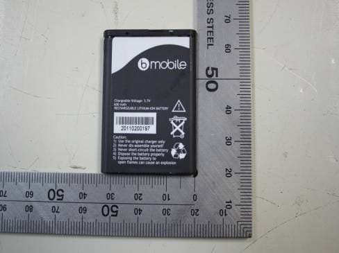
Click to zoom
Application Details
- Equipment Class
- JBP - Part 15 Class B Computing Device Peripheral
- Date of Grant
- Apr 20, 2011
- Application Purpose
- Original Equipment
- Date of Application
- Apr 20, 2011
- Equipment Note
- MOBILE PHONE-GSM PORTION
- Country
- Hong Kong
Documents & Files
Document Text
Text extracted from the exhibit documents filed with the FCC. Open a document above to read the original.
Users Manual
-1- User Manual -2- WELCOME! PLEASE READ THIS INFORMATION BEFORE USING THE PHONE. B-MOBILE® IS NOT RESPONSIBLE FOR ANY DAMAGE/S DUE TO MISINTERPRETATION OF THIS INFORMATION AND MISUSE OF PRODUCT. B-MOBILE™ aims to improve its products and services and reserves all rights to revise/change the description of this product and its software as well as this user’s manual without obligation to notify any person of such revisions and changes. Some features introduced in this manual are network or subscription-dependent features. Please contact your service provider for more information. -3- 1 General Information 1.1 Profile Please read this pamphlet carefully in order to make your phone in perfect condition. Perfectly combining humanized design and fine art, this mobile phone provides a streamlined outlook, comfortable hand-feeling, pleasant sounds and MP3 player which bring convenience and fun to your work. Our company may change this mobile phone without prior written notice and reserves the final right to interpret the performance of this mobile phone. Due to different software and network operators, display on your phone may be different, refer to your phone for details. 1.2 Safety Information If your phone has lost or been stolen, notify the telecommunication office the SIM card is disabled (network support is required). This can avoid economic loss caused by unauthorized use. Please take measures as following to avoid your phone being unauthorized use: · Set PIN code of SIM card · Set phone password -4- 1.3 Safety warning and Attentions Safety warning Ø ROAD SAFETY COMES FIRST Do not use a hand-held phone while driving. Use hands-free fittings when calls are unavoidable while driving. In some countries, dialing or receiving calls while driving is illegal! Ø SWITCH OFF IN AIRCRAFT Wireless devices can cause interference in aircraft. Using a mobile phone in flight is illegal and risky. Please make sure that your mobile phone is powered off in flight. Ø SWITCH OFF BEFORE ENTERING RISKY AREAS Strictly observe the relevant laws, codes, and regulations on the use of mobile phones in risky areas. Turn off your mobile phone before entering a place susceptible to explosion, such as an oil station, oil tank, chemical plant or a place where a blasting process is under way. Ø OBSERVE ALL SPECIAL REGULATIONS Follow any special regulations in force in any area such as hospitals and always switch off your phone whenever it is forbidden to use it or, when it may cause interference or danger. Properly use your mobile phone near medical apparatuses, such as pacemakers, hearing aids and some other electronic medical devices, as it may cause interference to such apparatuses. Ø INTERFERENCE The conversation quality of any mobile phone may be affected by radio interference. An antenna is built inside the mobile phone and located below the microphone. Do not touch the antenna area during a conversation, lest that the conversation quality deteriorate. -5- Ø QUALIFIED SERVICE Only qualified personnel may install or repair phone equipment. Installing or repairing the mobile phone on your own may bring great danger and violates the warranty rules. Ø ACCESSORIES AND BATTERIES Use only approved accessories and batteries. Ø USE SENSIBLY Use only in a normal and proper manner. Ø EMERGENCY CALLS Ensure the phone is switched on and in service, enter the emergency number, e.g. 112, then press the Dial key. Give your location and state your situation briefly. Do not end the call until told to do so. Note: Just like all other mobile phones, this mobile phone does not necessarily support all the features described in this manual due to network or radio transmission problems. Some networks even do not support the emergency call service. Therefore, do not rely solely on the mobile phone for critical communications such as first aid. Please consult the local network operator. Precautions This mobile phone is well designed with fine art. Please exercise special care when using it. The following suggestions will help your mobile phone survive the warranty period and extend its service life: Ø Keep the mobile phone and all its fittings beyond children's reach. Ø Keep the mobile phone dry. Keep away from rain, moisture, liquid or other substances that may corrode electronic circuits. -6- Ø Do not use or store the mobile phone in dusty places, lest that active parts of the mobile phone be damaged. Ø Do not store the mobile phone in a high-temperature place. High temperature will shorten the life of electronic circuits and damage the battery and some plastic parts. Ø Do not store the mobile phone in a chilly place. Otherwise, moistures will be formed inside the mobile phone to damage electronic circuits when the mobile phone is moved to a constant temperature place. Ø Do not throw, knock or shock the mobile phone, as that will destroy the internal circuits and high-precision components of the mobile phone. 2 Your phone 2.1 Phone overview 2.2 Functions of Keys The mobile phone provides the following keys: u Left and right soft key The bottom line on the screen displays the functions of the Left and Right soft key. u SIM1 dial key(use same key with Left soft key) Press it to originate a call on SIM card 1 by entering the called number or selecting a contact from the phonebook; or press it to receive an incoming call; or press it in standby state to show the latest call records u SIM2 dial key -7- Press it to originate a call on SIM card 1 by entering the called number or selecting a contact from the phonebook; or press it to receive an incoming call; or press it in standby state to show the latest call records. u End key Press it to end a call being dialed or end an ongoing call; or press it to exit the menu and return to the standby state; or hold it for two or three seconds to power on or off the mobile phone. u Direction key Press them to scroll the options when browsing a function list. In edit state, press direc…
Text truncated - open the document above for the full version.
Cover Letter(s)
Global Mobile Communication (HK) ltd., FCC ID: ZFT-K107 POWER OF ATTORNEY April 18, 2011 Federal Communications Commission Authorization and Evaluation Division 7435 Oakland Mills Road Columbia, MD 21046 To Whom It May Concern: We, Global Mobile Communication (HK) ltd.,hereby authorize Shenzhen Super Test Service Technology Co., Ltd. (Terry YANG/ Manager) located at No.5, Langshan 2nd Rd., North Hi-Tech Industrial Park ,Nanshan, Shenzhen, Guangdong ,China on our behalf, to apply to the Federal Communications Commission on our equipment. Any and all acts carried out by Shenzhen Super Test Service Technology Co., Ltd. (Terry YANG/ Manager) on our behalf shall have the same effect as acts of our own. This authorization expires on May 31, 2011. This is to advise that we are in full compliance with the Anti-Drug Abuse Act. We, Global Mobile Communication (HK) ltd.,are not subject to a denial of federal benefits pursuant to Section 5301 of the Anti-Drug Act of 1988, 21 USC853a, and no party to the application is subject to a denial of federal benefits pursuant to that section. ChunLu Guo Sales Global Mobile Communication (HK) ltd., April 18, 2011
External Photos
Report No: KS110407B02 Date of Issue: April 13, 2011 FCC ID: ZFT-K107 EXTERNAL PHOTOGRAPHS OF EUT Report No: KS110407B02 Date of Issue: April 13, 2011 FCC ID: ZFT-K107 Report No: KS110407B02 Date of Issue: April 13, 2011 FCC ID: ZFT-K107 Report No: KS110407B02 Date of Issue: April 13, 2011 FCC ID: ZFT-K107 Report No: KS110407B02 Date of Issue: April 13, 2011 FCC ID: ZFT-K107 Report No: KS110407B02 Date of Issue: April 13, 2011 FCC ID: ZFT-K107
Internal Photos
Report No: KS110407B02 Date of Issue: April 13, 2011 FCC ID: ZFT-K107 INTERNAL PHOTOGRAPHS OF EUT Report No: KS110407B02 Date of Issue: April 13, 2011 FCC ID: ZFT-K107 Report No: KS110407B02 Date of Issue: April 13, 2011 FCC ID: ZFT-K107 Report No: KS110407B02 Date of Issue: April 13, 2011 FCC ID: ZFT-K107 GSM antenna
Operational Description
1/2 Operation Description OPERATIONAL DESCRIPTION APPLICANT: Global Mobile Communication (HK) ltd., Manufacturer: Water World Technology Co., ltd FCC ID:ZFT-K107 Instruction Book: Users Manual Frequency Range GSM Transmit Frequency Band: 824.2-848.8 MHz Receive Frequency Band: 849.2-893.8 MHz Transmit Frequency Band: 1850.2-1909.8 MHz Receive Frequency Band: 1930.2-1989.8 MHz Specific Operating Power Range: Power Class 1; Power Control Level 0 +30dBm +2.0dB/-2.0dB Power Control Level 1 +28dBm +3.0dB/-3.0dB Power Control Level 2 +26dBm +3.0dB/-3.0dB Power Control Level 3 +24dBm +3.0dB/-3.0dB Power Control Level 4 +22dBm +3.0dB/-3.0dB Power Control Level 5 +20dBm +3.0dB/-3.0dB Power Control Level 6 +18dBm +3.0dB/-3.0dB Power Control Level 7 +16dBm +3.0dB/-3.0dB Power Control Level 8 +14dBm +3.0dB/-3.0dB Power Control Level 9 +12dBm +4.0dB/-4.0dB Power Control Level 10 +10dBm +4.0dB/-4.0dB Power Control Level 11 +8dBm +4.0dB/-4.0dB Power Control Level 12 +6dBm +4.0dB/-4.0dB Power Control Level 13 +4dBm +4.0dB/-4.0dB Power Control Level 14 +2dBm +5.0dB/-5.0dB Power Control Level 15 +0dBm +5.0dB/-5.0dB Note; Effective radiation efficiency is –3.7dB DC Voltage and Current into the Final Amplifier Module: Supply Voltage = 5.0Vdc Supply Current = ~0.5Amp. Tune-up Procedure: Tune-up Procedure Equipment Identification: Equipment's Identification label and its intended Location are as shown in EXHIBIT Type “ID Label / Location Information” (FCC ID Nameplate), and in EXHIBIT Type “Internal Photo”(Photograph of inside) Photographs: A complete set of the Photographs showing External and Internal Views of Circuit Details and Construction are provided by from EXHIBIT Type “External Photos” and “Internal Photos”. Accessories: Accessories 2/2 Operation Description Figure 1.2: Terminal Components (Accessories) Technical Descriptions TX synthesizer uses an Offset-PLL circuit. The Offset-PLL circuit consists of PLL-IC and TX_VCO and loop filter. Reference frequency of the above synthesizers is 26MHz and generated by VCTCXO. Control signal is sent from Baseband section and keeps frequency stability. TX IQ signal is input from Baseband section to MT6235, The Bluetooth signal is input form MT6601 and FM signal is input form TLG1120 section to MT6235. TX IQ signal is applied to the quadrature up-converter, and the up-converter LO signal is generated from the transceiver VCO within MT6139B. This up-converter translates the GMSK-modulated signal to an intermediate frequency (IF) that forms one input to a frequency/phase detector circuit. This IF signal is the reference input to an Offset-PLL circuit. The feedback path of this Offset-PLL circuit includes a down-conversion from the RF output frequency range to the IF range. The two inputs to this down-conversion mixer are formed the TX_VCO output and the LO generation circuits. The mixer output is the offset feedback signal that forms the variable input to a frequency/phase detector circuit. The detector compares its variable input to its reference input and generates an error signal that is low-pass filtered by the loop filter and applied to TX_VCO to force the RF frequency in the direction that minimizes errors. The TX_VCO output passes PA, Antenna SW, Coaxial connector with switch and emitted from embedded antenna. Digital Modulation: Analog speech produced by a microphone is encoded to digital PCM samples using a CODEC. The PCM samples are passed to a Vocoder for AMR (Advanced Multi Rate) encoding, to compress the speech samples. The encoding rate is determined by the Vocoder which formats the speech samples as data packets. A new data packet with data rate information is read by the microprocessor every 20 ms. The speech CODEC becomes AMR, FR(Full Rate), EFR(Enhanced FR) and HR(Half Rate). The microprocessor then sends the data packet to the transmit subsystem, and passed DAC to covert analog signal. I/Q base band signal is filtered and is inputted into 6M4003 containing quadrature phase modulator. Battery AC Charger
Parts List/Tune Up Info
037,22nF,±10%,16V,X7R,04024C25,C204,C212,C221 038,100nF,±10%,10V,X5R,040212C200,C206,C217,C61,C600,C800-C801,C400,C501,C30,C802,C803 035,1nF,±10%,50V,X7R,04024ED2,ED415,ED416,C449 036,10nF,±10%,16V,X7R,04022C38,C300 033,470pF,±10%,50V,X7R,04021C44 034,680pF,±10%,50V,COG,04022C402-C403 031,47pF,±5%,50V,COG,04021C614 032,100pF,±5%,50V,COG,04029C250,C13,C15,C219,C607,C406-C407,C409,C1243 029,33pF,±5%,50V,COG,040220C3-C4,C14,C19-C21,C26,C28-C29,C31-C33,C47-C50,C208,VR2,C10,C 35 030,39pF,±5%,50V,COG,04022ED201,ED203 027,22pF,±5%,50V,COG,04024C40,C601,C7,C203 028,27pF,±5%,50V,COG,04021C23 025,10pF,±5%,50V,COG,04021C401 026,12pF,±5%,50V,COG,04024ED3-ED6 023,4.7pF,±0.5pF,50V,COG,04021C418 024,6pF,±0.5pF,50V,COG,04023C606,C611,C410 021,2.2pF,±0.25pF,50V,COG,04024C404-C405,C432,C433 022,3.3pF,±0.25pF,50V,COG,04025C639,C642-C644,C8 019,150K ohm,±5%,1/16W,04021R36 020,18pF,±5%,50V,COG,04025C411,C414-C417 017,75K ohm,±5%,1/16W,04022R18,R215 018,100K ohm,±5%,1/16W,04022R214,R6 015,33K ohm,±5%,1/16W,04022R14,R213 016,47K ohm,±5%,1/16W,04022R5,R20 013,10K ohm,±5%,1/16W,04021R16 014,15K ohm,±5%,1/16W,04021R603 011,4.7K ohm,±5%,1/16W,04022R40,R41 012,6.8K ohm,±5%,1/16W,04023R201,R24,R502 009,1.5K ohm,±5%,1/16W,04023R203,R207,R19 010,2K ohm,±5%,1/16W,04021R206 007,510 ohm,±5%,1/16W,04022R200,R209 008,1K ohm,±5%,1/16W,040211R2,R8,R204,R440-R441,R1,R15,R231,R405,R407-R408 005,33 ohm,±5%,1/16W,04027R11,R13,R17,R64-R65,R7,R202 006,100 ohm,±5%,1/16W,04022R205,R208 003,0.36 ohm,±1%,1/4W,08051R300 004,10 ohm,±5%,1/16W,04021R35 001,0 ohm,±5%,1/16W,040211C419,LZ7,R4,R26,R601,R500,R504,R70,R71,R9(),R3() 002,0 ohm,±5%,1/10W,06031R406 BOOM NODescriptionQuatityLocation 079(T),RN1411,SC-59,Toshiba1Q5 077(S)LED(),0603,HT-193NB5,HARVATEK4LD1,LD4-LD5,LD34 078(T),DTC114TKA,SC-59,ROHM1Q5 075(S)LED(),0603,BL-HB336G-TRB,BRIGHT4LD1,LD4-LD5,LD34 076(S)LED(),0603,LTST-C193TBKT-5A,LITE-ON4LD1,LD4-LD5,LD34 073(S),,200mA,SOD523,RB521S-30TE61,ROHM1D413 074(S),,200mA,SOD523,DSF521,TOSHIBA1D413 071(S)IC,MOSFET WITH SCHOTTKY,DFN3x2-8L,SSF4703DC,SILIKRON1Q301 072(S),,200mA,SOD-523,SIG631E30T1G,SIG1D413 069(S)IC,MOSFET WITH SCHOTTKY,WPM2005B-8/TR,DFN3x2-8L,WILL1Q301 070(S)IC,MOSFET WITH SCHOTTKY,DFN3x2-8L,BF9024SPD-M,BYD1Q301 067(T)IC,MOSFET WITH SCHOTTKY,DFN3x2-8L,TPCF8B01,TOSHIBA1Q301 068(S)IC,MOSFET(P-Channel),WDFN-8L3x2,RP1800CGQW,RICHPOWER1Q301 065(S),5.5V,0402,AVLC5S02050,AMOTECH3ED10,ED220-ED221 066(S),5.5V,0402,ICVS0505500FR,ICT3ED10,ED220-ED221 063(S),,1.8K ohm,50mA,0402,MGGB1005M182HT-LF,4LZ3-LZ5,L800 064(S),5.5V,0402,SDV1005E5R5C400NPTF,Sunlord3ED10,ED220-ED221 061(N),1.8K ohm,50mA,0402,HZ1005K182TF,SUNLORD4LZ3-LZ5,L800 062(N),1.8K ohm,50mA,0402,BLM15HD182SN1,Murata4LZ3-LZ5,L800 059(S),1000 ohm,250mA,0402,BLM15HD102SN1,MURATA1C45 060(S),1000 ohm,250mA,0402,HZ1005K102TFB01,SUNLORD4LZ201,LZ202,LZ207-LZ208 057(S),75 ohm,300mA,0402,BLM15BB750SN1D,MURATA2LZ1-LZ2 058(S),75 ohm,300mA,0402,MGSB1005A750T-LF,2LZ1-LZ2 055,100nH,±5%,0402,MGCI1005TR10JT-LF,1L1 056(S),75 ohm,600mA,0402,SZ1005G750TF,SUNLORD2LZ1-LZ2 053,15nH,±5%,0402,MGCI1005T15NJT-LF,1L403 054,100nH,±5%,0402,SDCL1005CR10JTDF,SUNLORD1L1 051,10nH,±5%,0402,MGCI1005T10NJT-LF,1L400 052,15nH,±5%,0402,SDCL1005C15NJTDF,Sunlord1L403 049,4.7nH,±0.3nH,0402,MGCI1005T4N7ST-LF,1C463 050,10nH,±5%,0402,SDCL1005C10NJTDF,Sunlord1L400 047,6.2nH,±5%,0402,MGCI1005T6N2JT-LF,3C619,L406,L407 048,4.7nH,±0.3nH,0402,SDCL1005C4N7STDF,Sunlord1C463 045,2.4nH,±0.3nH,0402,MGCI1005T2N4ST-LF,1C618 046,6.2nH,±0.3nH,0402,SDCL1005C6N2STDF,SUNLORD3C619,L406,L407 043,10uF,±20%,6.3V,X5R,08057C11,C609,C201,C213,C211,C303,C624 044,2.4nH,±0.3nH,0402,SDCL1005C2N4STDF,SUNLORD1C618 041,2.2uF,±10%,6.3V,X5R,06038C218,C9,C60,C304-C305,C308-C310 042,4.7uF,±10%,6.3V,X5R,06032C57,C202 039,1uF,±10%,10V,X5R,06034C5,C58-C59,C56 040,1uF,±10%,6.3V,X5R,040213C1,C24,C41,C608,C613,C2,C17,C46,C51,C420-C423 119,3.9nH,±0.3nH,0402,MGCI1005T3N9ST-LF,1C37 120,18nH,±5%,0402,SDCL1005C18NJTDF,Sunlord1L402 117(T)P-FET(-20V,-1.37A),SIS4101PT1G,SOT-323,SIG1Q1 118,3.9nH,±0.3nH,0402,SDCL1005C3N9STDF,Sunlord1C37 115,0.5pF,±0.25pF,50V,COG,04021L452 116(T)P(-20V,-1.4A),WPM1480-3/TR,WILL1Q1 113PCB,7707-MB-V1.31 114(S),,,24.32x12.95x1.8mmH,77071 111(S),26MHz,±10ppm,9pF,3225,X3S026000B91H-NZ,HARMONY1X400 112(S),26MHz,±10ppm,9pF,3225,7M26000056,TXC1X400 109(S),26MHz,±10ppm,8.0pf,3225,X1E000021002200/TN4-26245,EPSON1X400 110(S),26MHz,±10ppm,7.4pF,3225,CX3225SB26000C4FZF06,KYOCERA1X400 107(S),32.768KHz,±20ppm,12.5pF,SSP-T7-F,SII1X200 108(S),32.768KHz,±20ppm,12.5pF,MS3V-T1R,MICRO1X200 105(T)MINI USB,12PIN,2.0mmH,TDUB01-BK5000,1USB400 106(S),32.768KHz,±20ppm,12.5pF,Q13MC1462000200(Q13MC1461000200), EPSON 1X200 103(S)Mini USB,12PIN,2.0mmH,MICFS-01215-TP03(UAF05-12204- 1501),LCN 1USB400 104(T)MINI USB,0.5PITCH,12PIN,2.0mmH,WKUBI008-001,1USB400 101(S)T-FLASH,,1.93mmH,WKTFH010-S01,JTCONN1TF100 102T-FLASH,,1.9mmH,TDTS01-8K5000,1TF100 099(S)SIM,,1.80mmH,TDSM01-6K5000,1SIM1 100(S)T-FLASH,,14.5x13.6x1.9mmH,CAH11-08193-SF01,LCN1TF100 097(S)SIM,,16.4x16.3x1.80mmH,SIMMS-00615-TP31(CAF99- 06183-1503),LCN 1SIM1 098SIM,,16.1x16.4x1.8mmH,WKSM010-1911,1SIM1 095(S),,,3PIN,3.0PITCH,8.4x3.5x6.2mmH,WKBAV006- D31P,JTCONN 1U9 096,,3.0PITCH,8.4x3.5x6.2mmH,TDBT01-3K5000,1U9 093(S)IC,,AB,UTQFN-9L,SN4990AIF09E,SI-EN1U201 094(S),,3.0PITCH,8.4x3.5x6.2mmH,PAN30-03626-1500,LCN1U9 091(S),SAW,EGSM/DCS RX,SFR942PY002,WISOL1U405 092(S)IC,MCP(32Mb+16Mb),ADMUX,M36W0R5040U6ZS L0,NUMONYX1U406 089(S),SAW,EGSM/DCS RX,EFCH9418TDL1,PANASONIC1U405 090(S),SAW,EGSM/DCS RX,SAWEN942MCN0F00,MURATA1U405 087(T)IC,FM,BK1080QB,QFN24,BEKEN1U1402 088(S)IC,,GSM,QFN-40,QS518,1U404 085(T)IC,,GSM,AM7803P,AMALFI1U601 086(N)FM,4x4mm,RDA5802E,RDA1U1402 083(T)IC,,SC6600L3(SC6600H3),1U100 084(S)IC,,SC6600L2,1U100 081(S),TVS,7V,65pf,SOD523,ESD5Z7.OT1G,ONSEMI1TVS301 082(S),TVS,7V,65pf,SOD-523,SIG5E7.OT1G,SIG1TVS301 080(S),TVS,5V,80pf,SOD523,ESD5Z5.0T1G,ONSEMI1TVS301 123(S),SAW,PCS1900-RX,SF14-1960M5UB50/A1,KYOCERA1U400 121,18nH,±5%,0402,MGCI1005T18NJT-LF,1L402 122(S),SAW,850-RX,SF14-0881M5UB50/A1,KYOCERA1U401 TypeManufactu…
Text truncated - open the document above for the full version.
Parts List/Tune Up Info
PDF 文件使用 "pdfFactory Pro" 试用版本创建 www.fineprint.cn PDF 文件使用 "pdfFactory Pro" 试用版本创建 www.fineprint.cn
Parts List/Tune Up Info
Tune UP 1 Adjustment of RF Output Power: (1) The equipment setup as shown in Figure 1. (2) Operation of PC adjusts equipment. (3) Use RF Engineering Tools at PC side. Select GSM850 Band: 1) Set GSM850 Band. 2) Set ARFCN: 190 3) TX ON. 4) Adjust the power to 32.4dBm (Power control level: PCL=5) by PA DAC value. 5) Repeat 4) for 15 times,and adjust the power level to 30.5, 28.8, 27, 25, 23, 21, 19, 17, 15, 13, 11, 9, 7, 5. 6) Make 16 Ramp-Up/Ramp-Down data from the adjustment value of (5) and (6). PC RF Tester GPIB Cable UART Cable RF Cable Test sample Figure 1 7) Data of 5) and 6) is writen to flash memory. Select PCS1900 Band: 1) Set PCS Band. 2) Set ARFCN: 661. 3) TX ON. 4) Adjust the power to 29.0 dBm (Power control level: PCL=0) by PA DAC value. 5) Repeat 4) for 15 times,and adjust the power level to 27.5, 26, 24, 22, 20, 18, 16, 14, 12, 10, 8, 6, 4, 2, 0. 6) Make 16 Ramp-Up/Ramp-Down data from the adjustment value of (5) and (6). 7) Data of 5) and 6) is writen to flash memory. 2 Adjustment of oscillation frequency of VCXO: (1) The equipment setup as shown in Figure 1. (2) Use Crystal AFC Control Tools to Set CapID and AFC DAC value. (3) Set Band=GSM850,Set ARFCN=190,Set PCL=12. 1) Set AFC DAC=4096,fixed.(Check that Vafc=1.4V). 2) Set CapID=0, and verify that frequency error >>10KHz. 3) Set CapID=63, and verify that frequency error <<-10KHz. 4) If the above 3 items are verified, then change CapID value to make frequency error be closed to 0 Hz as possible, record this CapID value. 5) Set CapID value got from step 4), then change AFC DAC value to make frequency error be closed to 0 Hz as possible, record this AFC DAC value. 6) Download the CapID value and AFC DAC value to flash memory. 3 Adjustment of RX Sensitivity: (1) Select GSM850 Band: 1) Set BCCH level:-85dBm;ARFCN:128. 2) Test sample make a call to connect RF Tester.. 3) Set TCH level:-106dBm. 4) Measure BERII error at TCH ARFCN:128, 190,251. 5) Tuen up the RX matching cricuit to make sure BERII<2% at each ARFCN. (2) Select PCS Band: 1) Set BCCH level:-85dBm;ARFCN:512. 2) Test sample make a call to connect RF Tester.. 3) Set TCH level:-106dBm. 4) Measure BERII error at TCH ARFCN:512, 661, 810. 5) Tuen up the RX matching cricuit to make sure BERII<2% at each ARFCN.
Schematics
SHEET: 4 OF 17 CONFIDENTIAL AND PROPRIETARY COMPANY: DEPARTMENT: DESIGNER: DATED: DATED: EQA: APPROVED: DATED: TITLE & REV: DOCUMENT NO.: APPROVED: ECO NO: LTR A B C D 6 5 4 3 2 1 DATE: D C B A REVISION RECORD 5.6nH C411Ë«Æμ ̧ijÉ5.6nH L406Ë«Æμ ̧ijÉ6.8NH V0.9 CLOSE TO RF FJX945/FAIRCHILD V8.0ÔÚV7.0μÄ»ù ́¡ÉÏÔö¼ÓBUFFER¡£ չѶμ÷ÊÔºóÐÞ ̧Ä 12mil 60mil 1800 900 850 1900 1900 850 C416£¬C417£¬C412£¬C454,L402,L407 U401£¬U403£¬C432£¬C433£¬C424£¬C451 Dual band NF part: change to small 0603 MHC:RF test point L406 6.2nH C414 18PF C415 18PF 1 CLK 2 DATA 3 NC 4 VDD_SYN 5 VDD_SYN_REG 6 VDD_LO 7 VDD_RF 8 TX_VCTRL 9 PA_VCTRL 10 US/EGSM_TX 11 DCS/PCS_TX 12 VDD_RF2 13 PCS_RX+ 14 PCS_RX- 15 DCS_RX+ 16 DCS_RX- 17 EGSM_RX- 18 EGSM_RX+ 19 USGSM_RX- 20 USGSM_RX+ 21 VDD_BB1 22 RX_CAP_Q- 23 RX_CAP_Q+ 24 RX_CAP_I- 25 RX_CAP_I+ 26 VDD_BB2 27 Q- 28 Q+ 29 I- 30 I+ 31 CLK_EN 32 REF_26/13B 33 REF_OUT 34 VDD_DCXO 35 REF_IN+ 36 REF_IN- 37 DCXO_REG 38 TEMP_OUT 39 VDD_IO 40 LE 41 GND U404 QS518 2 1 4 3 X400 26MHZ L402 15nH-18nH C432 2.2PF L403 15nH C405 2.2PF C404 2.2PF 1 DCS_IN 4 EGSM_IN 7 EGSM_OUT 6 EGSM_OUT 9 DCS_OUT 8 DCS_OUT 10 GND 5 GND 3 GND 2 GND U405 900/1800M SAW C400 100nf C402 680pF C403 680pF C420 1uF C406 100pF C421 1uF C422 1uF C407 100pF C418 4.7PF C401 10PF C423 1uF C433 2.2PF L407 6.2nH C416 18PF C417 18PF L400 10nH C409 100pF L408 NC L401 NC C419 0R C410 6PF C411 18PF 1 INPUT 3 OUTPUT1 4 OUTPUT2 2 GND 5 GND U400 RF-SAW-SAFEB1G96FA0F00 PCS SAW 1 INPUT 3 OUTPUT1 4 OUTPUT2 2 GND 5 GND U401 RF-SAW-SAFEB881MFL0F00 850M SAW R405 1K R1 1K R407 1K R408 1K C449 1nF 1 1 E401 ANT1-7110 ANTENNA C:CADENCEPSD_14.2TOOLSCAPTURELIBRARYDISCRETE.OLB 1 1 E402 ANT1-7110 ANTENNA C:CADENCEPSD_14.2TOOLSCAPTURELIBRARYDISCRETE.OLB R/C/L R3 0R/0603 GND 1 IN 2 OUT 3 4 5 6 J300 MHC-201 NC L452 0.5PF C463 4.7nH MHC RF TEST POINT R9 0R C608 1uF R601 1K--0R R603 10K--15K R605 15K---NC C613 1uF C607 100pF C601 22pF C609 22uF C611 6pF C606 5.6pF C618 0R--2.4nH C614 220pF--47pF C619 0R-6.2nH 1 VBAT2 2 GND 3 BAND_SEL 4 HB_IN 5 LB_IN 6 GND 7 TX_EN 8 VRAMP 9 GND 10 GND 11 GND 12 GND 13 GND 14 GND 15 RX4(850) 16 GND 17 RX2(GSM) 18 RX3(1900) 19 RX1(1800) 20 VBAT1 21 GND 22 GND 23 ANT 24 GND 25 SW1 26 GND 27 SW2 28 (NC)SW3 29 GND 30 GND 31 GND 32 GND U601 AM7803 C642 NC--3.3pF C639 NC--3.3pF C643 NC--3.3pF C644 NC--3.3pF C37 3.9nH C40 22PF L2 nc L3 nc R21 nc 1 2 3 Q3 2SC4774/ROHM R12 100pF R23 510R R25 33R R28 10K R33 0R C450 NC CLK_26M_BT [1] CLK_26M [2] CLK_26M_BT [1] BT_26MHZ [8] VDDRF [1,2] GND GND GND GND GND RFTX_HB [1] RFTX_LB [1] PA_EN [3] RF_PABAND [3] RF_RAMP [2] GND VBAT [2,4,6,7,8,9] GND GND GND RFTX_LB [1] RFTX_HB [1] RX/TXQN [2] RX/TXQP [2] RX/TXIN [2] RX/TXIP [2] VDDRF VDDRF VDDRF VDDRF VDDIO RFSEN [3] RFSCK [3] RFSDA [3] SC6600L_SP6601L_SCH_V1.0.3 Hardware RD. REVISION RECORD A B C D DATE: 1 2 3 4 5 6 D C B A LTR ECO NO: APPROVED: DOCUMENT NO.: TITLE & REV: DATED: APPROVED: EQA: DATED: DATED: DESIGNER: DEPARTMENT: Spreadtrum communications, Inc. COMPANY: CONFIDENTIAL AND PROPRIETARY SHEET: 2 OF 17 չѶ½ ̈ÒéisenseÏßÉÏÃæ ́®ÁªÒ» ̧ö10Å·Ä·μç×è should afford 100mA current CHARGE All trace connectted to the MOSFET should be as wide as possible should afford 1A current should afford 1A current 2009/03/23 2009/03/23 Guobing.Luan Wind.Deng Young.Wang 2009/03/23 E-HW-SC6600L-SCH-2008-0001 V0.9 1 IN 4 OUT 2 NC 3 NC X200 32.768KHZ C7 22PF C203 22PF C8 0.1uF R202 33R R7 33R C211 10uF C17 1uF R201 6.2K C38 10nF R16 10K C44 470pF C45 1nF---1K ́ÅÖé C46 1uF C51 1uF WHTLED SIM1 AUDIO RF ADC RTC SIM0 CLK USB H2 VCOM F3 AIL1 G3 AIR1 K1 AOM G2 MICN J7 AUXSPN J6 AUXSPP H6 HEAD_P_R F1 AUXMICN G1 MICP G6 HEAD_P_L F2 AUXMICP H1 MICBIAS C2 ADCI1 B1 ADCI0 B3 PAGSM B6 TXIN B5 TXREF A7 TXIP C6 TXQP N2 RTC32KO M1 VDDRTC C5 TXQN N1 RTC32KI L2 PADP_USB M2 VBATBK L1 PADM_USB A8 MCLKI M3 VDDUSB D1 WHTLED_IB3 D2 WHTLED_IB2 E1 WHTLED_IB1 E3 WHTLED_IB0 D3 WHTLED_RSET E2 HEADMIC_IN K7 EARN K6 EARP N3 SIMRST0 P2 SIMCLK0 P3 SIMDA0 P1 VSIM0 R1 VSIM1 T1 SIMDA1 R2 SIMCLK1 T2 SIMRST1 U100-B IC-BB-GSM-SC6600L1-224 C56 1uF R19 1.5K R231 1K C57 4.7uF C304 2.2uF C58 1uF,0603 C59 1uF,0603 C300 10nF C60 2.2uF C308 2.2uF C303 10uF AVDD36_3 GND CHARGE VBAT AVDD36_2 AVDD36_1 C1 AVDDVBO F11 AVDDAUX1 A6 VDD V2 VSSIO U1 VSS T11 VSS K12 VSSIO A1 AVDD36_2 C16 VSSIO C11 VSS C8 VSSIO C7 VSS T7 VDD F10 AVDDAUX2 B2 AVDD36_1 A2 AVDDRF A11 VCAM A9 VDDIO K13 VBAT J13 VMEM K10 VSS T12 VDD A5 VBAT A4 VMEM K9 VSS J10 VSS J9 VSS G7 VSS A3 AVDDBB C4 AGNDBB K2 VCHG K3 ISENSE L3 VDRV T9 VDDIO G13 VSS R3 VBAT B4 VBAT C3 AVDD36_3 F16 VDD J3 VSSAO J2 VDDAO L6 VIBR_OUT M6 VIBR_VSS N6 KPLED_OUT H3 AGNDVB J1 AVDDVB V1 NC U100-C IC-BB-GSM-SC6600L1-224 C309 2.2uF C310 2.2uF C305 2.2uF TVS301 TVS-ESD5Z5.0T1G ESD5Z5.0T1G C61 0.1uF R300 0.36R A K G S D A A S G D D C C Q301 TPCF8B01-1206A R36 150K ED10 C11 10uF 1 VBAT 2 ID 3 GND 4 NC 5 NC U9 BAT_PITCH3.0_2_STANDARD R406 18R,0603 D413 RB520S-30 MOT400 C10 100nF C9 2.2uFX5R R35 10R ADC1 ADC0 VCHG CHG_DRV [2] ISENSE [2] VBAT VBAT VCAM_CORE VCAM_ANA VDDRF AVDDBB AVDDVBO KPLED_CTRL [9] VBAT VBAT VDD_CORE VDDIO VMEM VCAM_ANA ISENSE [2] CHG_DRV [2] VCHG VBAT LED1- [6] LED3- LED4- VBACKUP 32K_IN [2] 32K_OUT [2] RX/TXQN [1] RX/TXQP [1] RX/TXIN [1] RX/TXIP [1] RF_RAMP [1] CLK_26M [1] RTCVDD SIM2RST [5] SIM2CLK [5] SIM2DA [5] VSIM2 VSIM SIMDA [5] SIMCLK [5] SIMRST [5] MICN [7] MICP [7] AUXMICN [7] AUXMICP [7] RECN [7] RECP [7] HEADPHR [7] HEADPHL [7] USB_DP [8] USB_DM [8] HEAD_MIC [7,8] AUXSPP [7] AUXSPN [7] MICBIAS VDD_USB AIL1 [8] AIR1 [8] 32K_IN [2] 32K_OUT [2] VBAT [1,2,4,6,7,8,9] VBAT [1,2,4,6,7,8,9] SC6600L_SP6601L_SCH_V1.0.3 CONFIDENTIAL AND PROPRIETARY COMPANY: Spreadtrum communications, Inc. DEPARTMENT: DESIGNER: DATED: DATED: EQA: APPROVED: DATED: TITLE & REV: DOCUMENT NO.: APPROVED: ECO NO: LTR A B C D 6 5 4 3 2 1 DATE: D C B A REVISION RECORD Hardware RD. SHEET: 1 OF 17 CAUTION: I2C has been pulled up by SC6600L, don't pull up it again DBB E-HW-SC6600L-SCH-2008-0001 2009/03/23 Young.Wang Wind.Deng Guobing.Luan 2009/03/23 2009/03/23 1 TP106 1 TP109 1 TP107 1 TP105…
Text truncated - open the document above for the full version.
Schematics
PDF 文件使用 "pdfFactory Pro" 试用版本创建 www.fineprint.cn PDF 文件使用 "pdfFactory Pro" 试用版本创建 www.fineprint.cn PDF 文件使用 "pdfFactory Pro" 试用版本创建 www.fineprint.cn PDF 文件使用 "pdfFactory Pro" 试用版本创建 www.fineprint.cn PDF 文件使用 "pdfFactory Pro" 试用版本创建 www.fineprint.cn PDF 文件使用 "pdfFactory Pro" 试用版本创建 www.fineprint.cn PDF 文件使用 "pdfFactory Pro" 试用版本创建 www.fineprint.cn PDF 文件使用 "pdfFactory Pro" 试用版本创建 www.fineprint.cn PDF 文件使用 "pdfFactory Pro" 试用版本创建 www.fineprint.cn PDF 文件使用 "pdfFactory Pro" 试用版本创建 www.fineprint.cn PDF 文件使用 "pdfFactory Pro" 试用版本创建 www.fineprint.cn
Test Report
Report No.: KS110407B02-EF FCC ID: ZFT-K107 Date of Issue: April 14, 2011 Page 1 / 28 FCC 47 CFR PART 15 SUBPART B TEST REPORT for Mobile Phone MODEL: K107, P30D Trade Name: B-mobile Test Report Number: KS110407B02-EF Issued to: Global Mobile Communication (HK) Ltd., 7/F,Kin On Commercial Building,49-51 Jervois Street,Sheung Wan,HongKong,China Issued by: Compliance Certification Services Inc . Linkuo Laboratory No. 81-1, Lane 210, Pa-De 2nd Rd., Luchu Hsiang, Taoyuan Shien, (338), Taiwan, R.O.C. TEL: 886-3-324-0332 FAX: 886-3-324-5235 Issued Date: April 14, 2011 Note: This report shall not be reproduced except in full, without the written approval of Compliance Certification Services Inc. This document may be altered or revised by Compliance Certification Services Inc. personnel only, and shall be noted in the revision section of the document. The client should not use it to claim product endorsement by , A2LA, NIST or any government agencies. The test results in the report only apply to the tested sample. Report No.: KS110407B02-EF FCC ID: ZFT-K107 Date of Issue: April 14, 2011 Page 2 This report shall not be reproduced except in full, without the written approval of Compliance Certification Services. Revision History Rev. Issue Date Revisions Effect Page Revised By 00 April 14, 2011 Initial Issue ALL Hadiif.Hoo Report No.: KS110407B02-EF FCC ID: ZFT-K107 Date of Issue: April 14, 2011 Page 3 This report shall not be reproduced except in full, without the written approval of Compliance Certification Services. TABLE OF CONTENTS 1 TEST RESULT CERTIFICATION................................................................................... 4 2 EUT DESCRIPTION........................................................................................................... 5 3 TEST METHODOLOGY ................................................................................................... 6 3.1. DECISION OF FINAL TEST MODE ....................................................................................................6 4 SETUP OF EQUIPMENT UNDER TEST ........................................................................ 7 4.1. DESCRIPTION OF SUPPORT UNITS................................................................................................ 7 4.2. CONFIGURATION OF SYSTEM UNDER TEST ................................................................................ 8 5 FACILITIES AND ACCREDITATIONS ......................................................................... 9 5.1. FACILITIES.......................................................................................................................................... 9 5.2. ACCREDITATIONS ............................................................................................................................. 9 5.3. MEASUREMENT UNCERTAINTY ...................................................................................................... 9 5.4. LIST OF TEST EQUIPMENT ............................................................................................................ 10 6 CONDUCTED EMISSION MEASUREMENT ...................…
Text truncated - open the document above for the full version.
Contact Information
Applicant
Chunlu Guo(Sales)
Test Firm
Compliance Certification Services (Kunshan) Inc.Eric Lin
Technical Specifications
| # | Rule Parts | Frequency Range | Power Output |
|---|---|---|---|
| 1 | 15B | - | - |
Other Applications from Global Mobile Communication (HK) Ltd.

ZFT-K105
Apr 24, 2011MOBILE PHONE-GSM PORTION
Equipment Class
PCE - PCS Licensed Transmitter held to ear