ZIHB831GSM Mobile Phone
Tech Vision Electronics Ltd.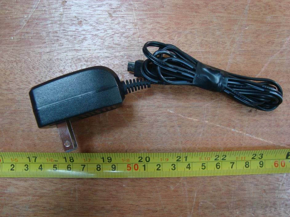
Click to zoom
Application Details
- Equipment Class
- DSC - Part 15 Security/Remote Control Transmitter
- Date of Grant
- Jun 15, 2011
- Application Purpose
- Original Equipment
- Date of Application
- Jun 15, 2011
- Equipment Note
- GSM Mobile Phone
- Frequency Range
- 433.91000000 - 433.91000000
- Company
- Tech Vision Electronics Ltd.
- Country
- China
Documents & Files
Document Text
Text extracted from the exhibit documents filed with the FCC. Open a document above to read the original.
Users Manual
USER GUIDE B831 Before operating this set, please read these instructions carefully. +S100 1 Warning: The torch uses a high-brightness LED. Do not shine directly into eyes, or view with optical instruments. NOTE – Remember to insert the battery before putting the handset on charge. IMPORTANT – Your handset is not supplied with a SIM card. The clam shell senior phone will work on all GSM mobile networks except “3”, and you will need to insert a SIM card for the handset to work correctly. Network Services – The clam shell senior phone is approved for use on the GSM850 and PCS1900 networks. Check with your mobile phone service provider to see if you can use the Dual-band feature or other Network Services described in this guide. Some networks may not support all language dependent characters and/or services. Where to find it................................................................... 3 Unpacking your clam shell senior phone In the box are: the mobile handset a mains power adaptor a rechargeable battery pack this user guide Keep the packing materials for future use. Keep your sales receipt - it is your guarantee. 2 Symbols on the display ...................................................... 4 Menu Operation .................................................................. 6 Read these notes first.......................................................... 6 Installation and setup.......................................................... 7 Switching On and Off .........................................................10 Making & answering calls...................................................11 Using the Phone Book & Fast keys (M1-M3).......................... 13 Volume control, Redial, Speakerphone, Mute (Secrecy) Call log.............................................................................16 SMS text messaging...........................................................17 Settings.............................................................................20 Phone (Language, Display, Security, Factory reset)... 20 Clock ...................................................... 20 Network ................................................ 20 Call ...................................................... 21 Sound.................................................... 21 Alarm............................................................................... 22 SOS Button.......................................................................23 Tools................................................................................26 Torch................................................................................27 FM radio............................................................................28 Health care........................................................................29 Troubleshooting............................................................... 30 Guarantee and Service information..................................... 31 Battery Information............................................................32 Additional Safety Information............................................. 32 Declaration of Conformity.................................................. 33 Contents 3 Emergencybutton (SOS) Press and hold 3sec to start SOS call procedure Where to find it Perform the function indicated on the LCD above. Talk button Press to answer a phone call. Press to enter redial list Press to dial a number Selection buttons ( - ) Up/Down button (^ / v ) Press to adjust receiving volume in talk and speakerphone modes. Press to step through names, phone numbers, menus and settings. Standby mode shortcuts: Up - to Sound Profiles Down - to Phonebook End / Power button (End call) Press to end or reject a call. Press to return to standby mode Press and hold to switch the phone on or off Earpiece Memory buttons M1,M2,M3 M1 / M2 / M3 3 memory locations for direct dial out. Torch Beam Visual Indicators Torch button Press and hold to switch the Torch on The Red LED is steady on during charging, and flashes when the battery is low. The Blue LED flashes when connected to the mobile network. The Green LED flashes when there is a missed call(s). Plug in headset accessory (not supplied) for headset use. Headset Connector Charging Connector Plug in power adapter to charge battery. Warning! The torch uses a high-brightness LED and you should not point the beam directly into eyes, or view with optical instruments. 4 Note: Press the SOS button on the SOS button on the wireless SOS bracelet ,the left LED will flash, If the left LED not flash, please replace the battery. Press and hold the SOS button on the wireless SOS bracelet, it will start the SOS function, when the left and right LED both flashed it means that the signal was successfully launched. (optional extra not always supplied, it is dependent on the particular commercial model.) Press and hold a few seconds to start SOS call procedure SOS button Left LED Right LED 5 Time Date Symbols on the display 1 - The left selection button in the idle mode is Menu. 2 - The right selection button in the idle mode is SMS. The Soft keys change to different functions in other modes. [Note: Symbols and positions on the display may vary.] Radio link/signal level - On steady when linked and shows the signal strength. Battery charge level - Charge handset as soon as possible if it shows nearly empty. While the batteries are being charged, this blinks. Roaming - On if roaming to other mobile network. Call Divert - On if call divert unconditional is set. Alarm - On if an alarm is set. Ringer off & vibrator off- On if handset's ringer and vibrator are both turned off. Ringer on & vibrator on - On if handset's ringer and vibrator are both turned on. The network name in service 1 2 6 Ringer off & vibrator on - On if handset's ringer is turned off and vibrator is turned on. Headset - On when a headset is plugged in. New SMS - Indicates you have new text messages. Full S…
Text truncated - open the document above for the full version.
Block Diagram
4 :0.0 XH Title: MODE: : : : 1 2 3 4 5 6 7 8 9 10 11 12 13 14 15 16 17 18 19 20 21 22 22 21 20 19 18 17 16 15 14 13 12 11 10 9 8 7 6 5 4 3 2 1 A B C D E F G H I J K L M N O O N M L K J I H G F E D C B A Y X 1 Tech-Vision Communications Ltd. MIC SIM CARD B831 MatthewChu Wanghuan GSM Block Diagram Infineon IC/PMB7880 V1.3 U2 Battrey Base band and RF transceiver KEYPAD GSM ANT Dispaly TX RX 850/1900 RF Swicth IC/B9506 SAW Filter 850/1900 RX TX IC/AX508 RF PA Speaker Receiver Ringer 26MHZ crystal 32.768KHZ crystal MOTO clock U3 850/900 1800/1900 850 1900 U1 UART PORT TXD RXD Headset mic Rec RDA5802E FM Broadcast FM_R/LOUT GSM 850:Tx:824 MHz~849 MHz Rx:869 MHz~894 MHz PCS 1900:Tx:1850 MHz~1910 MHz Rx:1930 MHz~1990 MHz 4 4 :0.0 433.91 RF WangHuan Tech-Vision Communications Ltd. X Y A B C D E F G H I J K L M N O O N M L K J I H G F E D C B A 1 2 3 4 5 6 7 8 9 10 11 12 13 14 15 16 17 18 19 20 21 22 22 21 20 19 18 17 16 15 14 13 12 11 10 9 8 7 6 5 4 3 2 1 : : : MODE: Title: B831 MatthewChu XH STC11L04E MCU CC1101 433 RF tranceiver 433.91_Antenna 433.91-RF_TRANSCEIVER I2S I2S U10 26 MHZ crystal U9
External Photos
EXHIBIT B - EUT EXTERNAL PHOTOGRAPHS EUT – Front View EUT – Rear View EUT – Side View EUT – Unfolded View EUT – Adapter 1# Side View EUT – Adapter 1# Logo View EUT – Adapter 2# Side View EUT – Adapter 2# Logo View
ID Label/Location Info
EXHIBIT A - FCC ID LABELING AND LOCATION FCC ID Label FCC ID Label Location Label here The label shown shall be permanently affixed at a conspicuous location on the device and be readily visible to the user at the time purchase (Labeling requirements per 2.925)
Internal Photos
EXHIBIT C - EUT INTERNAL PHOTOGRAPHS EUT – Battery off View EUT – Cover off View EUT – Main Board Top View EUT – Main Board Bottom View 433.91 Ant GSM Antenna EUT – Main Board without Antenna Bottom View EUT – Main Board Bottom Shielding off View 1 EUT – Main Board Bottom Shielding off View 2 EUT – LCD Top View EUT – LCD Bottom View EUT – GSM Antenna View EUT – Battery View
Operational Description
Operational description and technical overview for B831 GSM mobile phone B831 is composed of four parts, which are radio frequency parts, the CPU part, the interface part and 433.91 Transceiver RF section RF part of the module consists of three parts, ADG3232GC6T2LF, AX508, and SAW Filters. The RF signal is include receive signal and sends signal. Modules receiving the signal from the antenna then separate the send and receive signals by the internal antenna switch of R18 AX508. The received signals input the pin 9 of ANT, then feet out into the receiver front-end circuit from the pin6 and pin7 of R18. The working status of R18 is controlled by the CPU signals PAEN, BANDSW_DCS, VAPC, and VCXOEN. After the RF antenna switch inside the R18, two analog switches U102, U103 also will be used to separate the 850/900 and 1800 /1900 signals. Four Saw filter U2, U506, U507, U3 will be pass before the 850, 900, 1800, 1900 signals enter into the ADG3232GC6T2LF. After the processing of ADG3232GC6T2LF, signals will into the CPU. About the sending signals which processed by the CPU will be send into the ADG3232GC6T2LF, then feet into the power amplifier AX508 by the pin10 and pin11 of ADG3232GC6T2LF, the amplified signal sent by the antenna from the AX508. CPU part Based on a dual-processor architecture, PMB7880 integrate both an ARM7EJ-S core and 2 digital signal processor cores. ARM7EJ-S is the main processor that is responsible for running 2G and 2.5G protocol software. Digital signal processors handle the MODEM algorithms as well as advanced audio functions. Except for some mixed-signal circuitries, the other building blocks in PMB7880 are connected to either the microcontroller or one of the digital signal processor. The interface of PMB7880 control radio consists of Baseband Serial Interface (BSI), Baseband Parallel Interface (BPI), Automatic Power Control (APC) and Automatic Frequency Control (AFC) together with APC-DAC and AFC-DAC. PMB7880 also consist of the following subsystems: Microcontroller Unit (MCU) Subsystem Digital Signal Processor (DSP) Subsystem MCU/DSP Interface Microcontroller Peripherals Microcontroller Coprocessors DSP Peripherals Voice Front End Audio Front End Baseband Front End Timing Generator Power, Reset and Clock subsystem Power-on sequences, switches and SIM level shifters. Interface Section The interface of B831 includes the GPIO, UART, SIM Interface, POWER, AUDIO, RF Pad. The pins of AUDIO, GPIO, FM,SIM Interface are directly connect to the TP1. Between the RF antenna pad and the pin 11 of SKY77518 are connected by the capacitor C7. The POWER pins are directly power supply the R18, TP1. 433.91 Transceiver RF unit and MCU unit. CC1101 single chip FSK transceiver is used to perform all RF functions, Centre frequency is 433.91MHz. MCU(STC11L04E) is used to handle CC1101. and output power is 10dBm. Meanwhile, information was transmitted by antenna.
Schematics
Title: MODE: ::: 1 2 3 4 5 6 7 8 9101112 13141516171819202122 22 21 20 19 18 17 16 15 14 13 12 11 10 9 8 7 6 5 4 3 2 1 A BCDEFGH I J K L MN O O NM L K J I HGFEDCB A Y X 1 Tech-Vision Communications Ltd. ULC2 RF :0.0 6 WangHuan B831 MatthewChu 1 SH1 B820 RF SHIELD CAN C3647nF C56DNI C21DNI C35470pF C2427PF L4 3.9nH R14 0R R8 1K R3 0R 123 4 XTAL3 26Mhz +/-30PPM 10pF D10 VDD_DIG A11 VDD_LO F14 VDD_VCO A10 VDD_LRF_XO A8 XO A9 XOX A15 VSS_RF1 A12 VSS_RF2 B14 VSS_RF3 B13 VSS_RF4 B12 VSS_RF5 B10 VSS_RF6 C14 VSS_RF7 C10 VSS_RF8 D11 VSS_RF9 D14 VSS_RF10 E12 VSS_RF11 E13 VSS_RF12 E14 VSS_RF13 E15 RX34 D15 RX34X C15 RX12 B15 RX12X F15 VDD_LRF2V5 F13 VDD_RX A13 TX2 A14 TX1 P13 PAOUT1 D12 REXT B11 VDD_LRF1V5 C11 VDD_TRX U2-C IC--PMB7880 C644.7nF C346.8nF C6847nF C58 12pF C59 6.8pF C28 3pF +-0.25pF C31 3pF +-0.25pF C32 3pF +-0.25pF C33 3pF +-0.25pF L1 18nH L2 5.6nH C121uF C21uF C8100nF C10 1uF L3 8.2nH C53 1.8pF C54 1pF C2727pF C26 27pF L6 47nH L10 NC 12 34 5 6 SW24 MM8430-2610RA1 1 1800/1900RX 2 NC 3 850/900RX 4 VC1 5 1800/1900TX 6 GND1 7 850/900TX 8 GND2 9 ANT 10 VC2 11 NC1 12 GND4 U3 ICLMSP33AA-696 R1 0R R2 NC R10 NC R11 0R ANT1 TP98 TP17 C177pF HB LB 1 IN1 2 G1 3 G2 4 IN2 5 G3 6 OUT2 7 OUTX2 8 OUT1 9 OUTX1 10 G4 BPF1 B9500 C16 270pF AX508 15 VBAT 16 VBAT 17 VBAT 18 VBAT 23 VBAT 24 VBAT 26 VBAT 22 VBATC 11 HBOUT 19 TX_EN 8 VDD 12 DA 2 LBOUT 9 BS/VC2_IN 1 NC 3 NC 4 NC 10 VC1_IN 13 VC1_OUT 14 VC2_OUT 25 VAMP 5 VBAT 6 VBAT 7 VBAT 20 HB_IN 21 LB_IN 27 GND U1 C15 27p C66 47p C67 27p C63 82N C3 27p C14 27p L5 10nH C47 47uF GND [2] VC2 [2] VC1 VRF1 VRF2 VRF0 VD1 VRF0 VRF1 TP93 [2] TXON_PA [2] BS VBAT GSM 850:Tx:824 MHz~ 849 MHz Rx:869 MHz~894 MHz PCS 1900:Tx:1850 MHz~1910 MHz Rx:1930 MHz~1990 MHz GSM BB Title: MODE: ::: 1 2 3 4 5 6 7 8 9 10 11 12 13 14 15 16 17 18 19 20 21 22 22 21 20 19 18 17 16 15 14 13 12 11 10 9 8 7 6 5 4 3 2 1 A BCDEFGH I J K L MN O O NM L K J I HGFEDCB A Y X Tech-Vision Communications Ltd. :0.0 2 WangHuan 6 Flash elect B831 MatthewChu ASC SSC0 JTAG&DEBUGSIMVCXO I2CVOICEBAND KEYPAD RF CONTROL ADC P10 M2 R11 M7 R14 M0 N10 M9 A7 T_OUT0 B6 T_OUT2 A6 T_OUT3 A5 T_OUT4 B4 CLKOUTT R10 CCRST P7 CCLK N8 CCIN R8 CCIO M9 CCVZ_N K9 TRST_N R9 TCK P8 TDO M10 TDI P9 TMS C5 TRIG_IN F7 NMI_N B5 TRIG_OUT N6 MON1 N9 MON2 A4 CC00IO G8 CTS_N H8 RTS_N G7 RXD H7 TXD G6 SSC0_MTSR J6 SSC0_CLK H6 DISP_REST K6 SSC0_MRST H9 SCL H10 SDA G3 EFUSE F9 KP8 D8 KP7 C9 KP6 C6 KP5 D9 KP4 C7 KP3 B7 T_OUT8 C8 KP0 D6 KP1 D7 KP2 M14 EPPA1 M12 EPP1 N15 EPN1 A3 RSTOUT_N F8 KP9 R13 MICN1 P15 MICP1 R12 MICN2 P11 MICP2 P12 VMIC U2-A IC--PMB7880 R36 22K 1% C4 0603N 4.7uF R4 2.2K R613 1.5K C39 27PF C18 0805N 10UF C37 27PF R25 4.7R R22 4.7R R42 22K 1% C71 18pF C7018pF XTAL4 MS3V-T1R 32.768k LOUDSPEAKER DRIVERLDD SUPPLYANA POWER SUPPLYCHARGER RTCBUS CONTROL MEMORY DIG SUPPLY G9 VDD_MAIN_1 J7 VDD_MAIN_2 G10 VDD_PLL L4 VDDP_MEM R6 VDD_RTC R7 VDD_SIM F6 VDDP_IO B8 VSS_1 B9 VSS_2 J8 VSS_4 K8 VSS_5 K7 VSS_6 J12 W_LED_FBN J14 W_LED_FBP B3 BACK_LIGHT M8 VSS_9 F10 VSS_8 K12 VDD_LRTC B1 VIB_CTRL G12 VDD_LD1 M11 VDD_LSIM J10 VDD_LIO K15 VDD_LANA K10 VDD_LMEM J13 VDD_LBUF A2 W_LED_DRV B2 T2IN L12 VSS_EPLS K13 VSS_MS1 M15 VSS_MS2 L13 VSS_MS3 L14 VSS_MS4 N14 VSS_MS5 P14 VSS_MS6 N11 VSS_MS7 H13 VBAT1 F12 VBAT2 H15 VBAT3 H14 VBAT4 J9 CS H12 CDT L15 LOUD1 K14 LOUD2 A1 NC3 J15 NC2 R15 NC1 N7 SWITCH_ON G13 IREF G14 AGND G15 VREFP P5 RESET_N M7 SAFE_RES P6 OSC32K R5 F32K E3 BHE_N N5 OE_N E2 WR_N R3 RD_N M6 ADV_N M5 CS3_N K3 CS1_N P4 CS0_N M4 D15 J1 D14 K2 D13 L2 D12 N1 D11 M1 D10 R2 D09 P3 D08 J2 D07 K1 D06 M2 D05 L1 D04 N2 D03 P2 D02 P1 D01 R4 D00 C1 A08 F1 A09 F2 A10 G2 A11 H2 A12 J3 A13 H3 A14 J4 A15 K4 A16 L3 A17 F3 A18 D1 A19 H1 A20 E1 A21 G1 A22 R1 NC4 H4 A07 D2 A06 G4 A05 D4 A04 E4 A03 F4 A02 D5 A01 C2 A00 U2-B IC--PMB7880 C7 220nF C6 0603N 2.2uF C25 DNI C19 DNI C50 0603N 2.2uF C41 1nF R33 10K C5 27pF R12 1.2K C1 100nF C11 27pF C1327pF R37 1.2K C83100nF C84 100nF C92 100nF C93 100nF C44 1uF C43 1uF C38 1uF C51 1uF C46 1uF R13 0R R16 0R G2 DQ0 E3 DQ1 H3 DQ2 F4 DQ3 F5 DQ4 H6 DQ5 E6 DQ6 G7 DQ7 H2 DQ8 F3 DQ9 G3 DQ10 H4 DQ11 G6 DQ12 F6 DQ13 H7 DQ14 F7 DQ15 E1 A0 D1 A1 C1 A2 B1 A3 D2 A4 C2 A5 B2 A6 A2 A7 A6 A8 C6 A9 D6 A10 A7 A11 B7 A12 C7 A13 D7 A14 B8 A15 E8 A16 D3 A17 C3 A18 B6 A19 C5 A20 C8 A21 G5 VCCS G4 VCCF G8 VCC2 E2 VCC1 A5 WEN B3 UBN A3 LBN B4 RESETN F2 OEN A4 WPN_ACC C4 RY_BYN F1 CE1FN G1 CE1SN B5 CE2S F8 CIOF U5 TP16 R61 DNI C42 100nF R27 0R R29 0R R30 DNI R31 22K R38 22K R39 NC R41 nc R47 0R R9 470K R67 1K5 C9 10uF0805 BAT1 BATML414R-TT40A-TP1 GPIO_32 GPIO_38 GPIO_30 [5] KEYOUT0 [5] KEYOUT1 [5] KEYOUT2 [5] KEYOUT3 [5] KEYOUT4 [5] KEYOUT5 [5] KEYIN0 [5] KEYIN1 [5] KEYIN2 [5] KEYIN3 [4] TBAT [2,4] EXT_MIC [1] TXON_PA [1] VC1 [1] VC2 [1] BS [4] SIM_IO [4] SIM_CLK [4] SIM_RST [4] ULC2_TXD [4] ULC2_RXDHS_DET [2,4] EXT_MIC GND VANA [4] EPPA1 [3] FM_EN [4] MRST0 [3] LIGHT_LED1 [3] REC_N [3] REC_P GND GND [4,5] ON/OFF [4] HS_ID VBAT [3] SPK_P [3] SPK_N VRTC VSIM VD1 VIO VMEM VMEM VSIM VIO VD1 VANA VBUF [2] CS0 [2] CS1 [2,3] CS3 [2] RD [2,3] WR [2] OE [2] BHE [4] CHARGE_SWITCH [4] CHARGE_DET [2]A[0:22] [2]D[0:15] D0D1D2D3D4D5D6D7D8D9D10D11D12D13D14D15 A0A1A2A3A4A5A6A7A8A9A10A11A12A13A14A15A16A17A18A19A20A21A22 VRTC [5] KEYPAD_BL [4] VIB [3] I2C_SCL [3] I2C_SDA [3] LCM_BL_EN VRTC [3] MIC+ [3] MIC- [5] FLIP_SNS [2] A0 [2] BHE [2] CS1 [2] CS0 [2,3] WR [2] RD GND GND [2]D[0:15] D0D1D2D3D4D5D6D7D8D9D10D11D12D13D14D15 [2]A[0:22] A1A2A3A4A5A6A7A8A9A10A11A12A13A14A15A16A17A18A19A20A21A22 VMEM [2] OE [2,3] CS3 VMEM VMEM VIO VMEM [3] CLK_32K [5] EXT_INT VIO [3] DISP_RST [3] LIGHT_LED2 [3] LIGHT_LED3 Tech-Vision Communications Ltd. X Y A BCDEFGH I J K L MN O O NM L K J I HGFEDCB A 1 2 3 4 5 6 7 8 9101112 13141516171819202122 22 21 20 19 18 17 16 15 14 13 12 11 10 9 8 7 6 5 4 3 2 1 ::: MODE: Title: GSM FM 3 :0.0 WangHuan 6 MIC SPK/REC B831 MatthewChu C40 DNI 2 + 1 - MIC1 MICB4015AP423-71 D14 DF2S6.8FS D15 DF2S6.8FS 1 GND4 2 LNAN 3 RFGND 4 LNAP 5 GND1 6 XTAL 7 RST 8 SEN 9 SCLK 10 SDIO 11 RCLK 12 VIO 13 AVDD 14 GND2 15 ROUT 16 LOUT 17 GND3 18 DVDD 19 GPIO3 20 …
Text truncated - open the document above for the full version.
Test Report
Note: This test report is prepared for the customer shown above and for the device described herein. It may not be duplicated or used in part without prior written consent from Bay Area Compliance Laboratories Corp. This report must not be used by the customer to claim product certification, approval, or endorsement by NVLAP*, or any agency of the Federal Government. * This report contains data that are not covered by the NVLAP accreditation and are marked with an asterisk “★” (Rev.2) FCC PART 15.231 MEASUREMENT AND TEST REPORT For Tech Vision Electronics Ltd. Flat 209, 2/F, Jiuzhou Electric Building, Southern No.12 Rd., Hi-Tech Industrial Park, Nanshan District, Shenzhen, Guangdong, China FCC ID: ZIHB831 Report Type: Original Report Product Type: GSM Mobile Phone Test Engineer: Allan An Report Number: RDG11042704-15.231 Report Date: 2011-05-18 Reviewed By: Merry Zhao EMC Engineer Prepared By: Bay Area Compliance Laboratories Corp. (Shenzhen) 6/F, the 3rd Phase of WanLi Industrial Building, ShiHua Road, FuTian Free Trade Zone Shenzhen, Guangdong, China Tel: +86-755-33320018 Fax: +86-755-33320008 Tech Vision Electronics Ltd. FCC ID: ZIHB831 Report No.: RDG11042704-15.231 Page 2 of 22 FCC Part15.231 Test Report TABLE OF CONTENTS GENERAL INFORMATION.......................................................................................................................................3 PRODUCT DESCRIPTION FOR EQUIPMENT UNDER TEST (EUT) ....................................................................................3 OBJECTIVE...................................................................................................................................................................3 RELATED SUBMITTAL(S)/GRANT(S).............................................................................................................................3 TEST METHODOLOGY..................................................................................................................................................3 TEST FACILITY.............................................................................................................................................................3 SYSTEM TEST CONFIGURATION ..........................................................................................................................5 JUSTIFICATION.............................................................................................................................................................5 SPECIAL ACCESSORIES.................................................................................................................................................5 EQUIPMENT MODIFICATIONS.......................................................................................................................................5 CONFIGURATION OF TEST SETUP.................................................................................................................................5 BLOCK DIAGRAM OF TEST SETUP................................................................................................................................5 SUMMARY OF TEST RESULTS ...............................................................................................................................6 FCC §15.203 - ANTENNA REQUIREMENT.............................................................................................................7 APPLICABLE STANDARD..............................................................................................................................................7 FCC §15.207 – AC LINE CONDUCTED EMISSIONS .............................................................................................8 MEASUREMENT UNCERTAINTY....................................................................................................................................8 EUT SETUP..................................................................................................................................................................8 EMI TEST RECEIVER SETUP.........................................................................................................................................9 TEST EQUIPMENT LIST AND DETAILS...........................................................................................................................9 TEST PROCEDURE........................................................................................................................................................9 TEST RESULTS SUMMARY............................................................................................................................................9 TEST DATA..................................................................................................................................................................9 FCC §15.205, §15.209, §15.35(C) & §15.231(B) - RADIATED EMISSIONS.........................................................14 MEASUREMENT UNCERTAINTY..................................................................................................................................14 EUT SETUP................................................................................................................................................................14 EMI TEST RECEIVER SETUP.......................................................................................................................................15 TEST PROCEDURE......................................................................................................................................................15 APPLICABLE STANDARD............................................................................................................................................15 CORRECTED AMPLITUDE & MARGIN CALCULATION.................................................................................................15 …
Text truncated - open the document above for the full version.
Test Setup Photos
EXHIBIT D - TEST SETUP PHOTOGRAPHS AC Line Conducted Emissions - Front View AC Line Conducted Emissions - Side View Radiated Emission – Front View (Below 1 GHz) Radiated Emission – Rear View (Below 1 GHz) Radiated Emission – Front View (Above 1 GHz) Radiated Emission – Rear View (Above 1 GHz)
Contact Information
Applicant
Yin Zhang Hu(Project Manager)
Test Firm
Bay Area Compliance Laboratory Corp. (Shenzhen)John Chan
Technical Specifications
| # | Rule Parts | Frequency Range | Power Output |
|---|---|---|---|
| 1 | 15.231 | 433.91 MHz - 433.91 MHz | - |
Other Applications from Tech Vision Electronics Ltd.
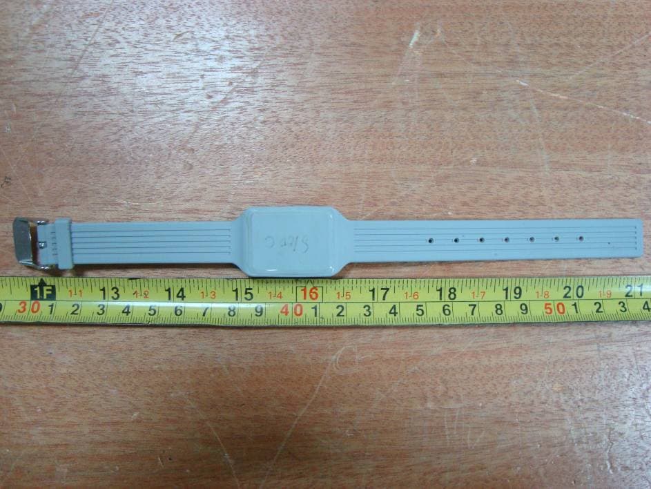
ZIHS100
Jun 15, 2011S100 Wireless SOS Health Bracelet
Equipment Class
DSC - Part 15 Security/Remote Control Transmitter