ZMOFIBOCOMG610Wireless Communication Module
Fibocom Wireless Inc.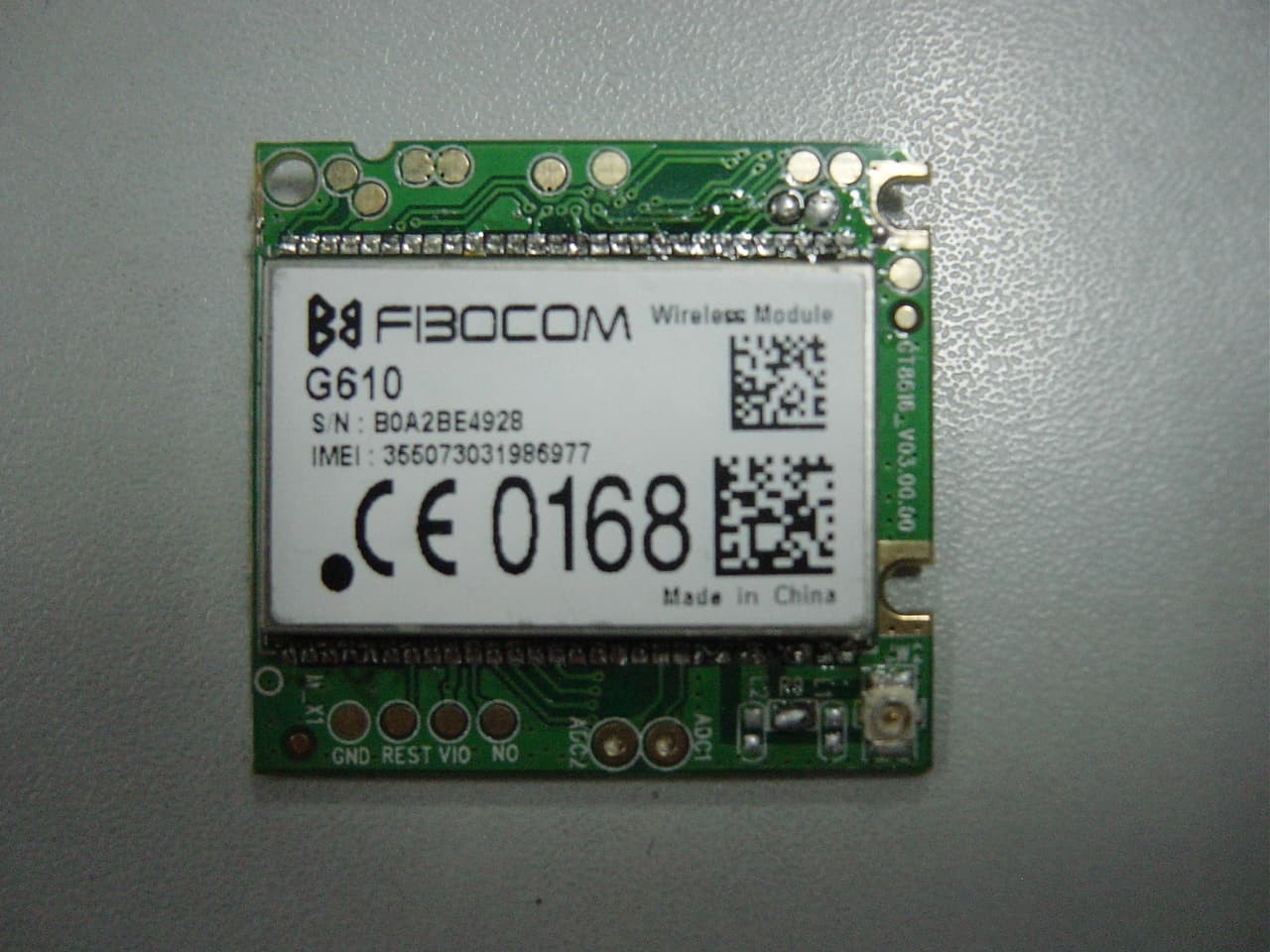
Click to zoom
Application Details
- Equipment Class
- PCB - PCS Licensed Transmitter
- Date of Grant
- Jul 11, 2011
- Application Purpose
- Original Equipment
- Date of Application
- Jul 05, 2011
- Equipment Note
- Wireless Communication Module
- Frequency Range
- 1850.20000000 - 1909.80000000
- Company
- Fibocom Wireless Inc.
- Country
- China
Documents & Files
Document Text
Text extracted from the exhibit documents filed with the FCC. Open a document above to read the original.
Users Manual
G610 GPRS Module Hardware User Manual Version: V1.0.2 Date: 2011-03-31 G610 GPRS Module Hardware User Manual Page 2 of 47 Confidential Material This document contains information highly confidential to Shenzhen G&T Industrial Development Co., Ltd (Fibocom). Fibocom offers this information as a service to its customers, to support application and engineering efforts that use the products designed by Fibocom. The information provided is based upon requirements specifically provided to Fibocom by the customers. All specifications supplied herein are subject to change. Disclosure of this information to other parties is prohibited without the written consent o f G & T. Copyright Transmittal, reproduction, dissemination and/or editing of this document as well as utilization of its contents and communication thereof to others without express authorization are prohibited. Offenders will be held liable for payment of damages. All rights created by patent grant or registration of a utility model or design patent are reserved. Copyright ©1999-2010 Shenzhen G&T Industrial Development Co., Ltd. All rights reserved. Revision History Version Date Remarks V1.0.2 2011-03-31 1. Update UART description 2. Fix HS_DET description Trademarks Notice The FIBOCOM Logo is registered by Shenzhen G&T Industrial Development Co., Ltd. All other product or service names or Logos are the property of their respective owners. Copyright ©1999-2010 Shenzhen G&T Industrial Development Co., Ltd. All rights reserved. G610 GPRS Module Hardware User Manual Page 3 of 47 Contents 1 Preface ................................................................................................................................................ 6 1.1 Manual Scope .......................................................................................................................... 6 1.2 Target Audience ....................................................................................................................... 6 1.3 Applicable Documents ............................................................................................................. 6 1.4 Standards ................................................................................................................................. 6 1.5 Regulatory Approvals ............................................................................................................... 7 1.6 FCC Notice to Users ................................................................................................................ 7 2 Introduction .......................................................................................................................................... 8 2.1 Product concept ....................................................................................................................... 8 2.2 Product Specifications .............................................................................................................. 9 3 Hardware Interface Description .........................................................................................................11 3.1 Architecture Overview .............................................................................................................11 3.1.1 Digital Block ..................................................................................................................11 3.1.2 Analog Block ................................................................................................................11 3.1.3 GSM Transceiver Block ............................................................................................... 12 3.2 Operating Modes .................................................................................................................... 12 3.3 Power Supply ......................................................................................................................... 13 3.3.1 Power Supply Design .................................................................................................. 13 3.3.2 Power Consumption .................................................................................................... 15 3.4 Power On/Off Operation ......................................................................................................... 16 3.4.1 Turning the G610 On ................................................................................................... 16 3.4.2 Turning the G610 Off ................................................................................................... 17 3.4.3 Turning the G610 Off Using AT Command ................................................................. 18 3.5 Sleep Mode ............................................................................................................................ 18 3.5.1 Activating Sleep Mode ................................................................................................ 19 3.5.2 Serial Interface during Sleep Mode ............................................................................. 19 3.5.3 Terminating Sleep Mode ............................................................................................. 20 3.6 Real Time Clock ..................................................................................................................... 22 3.6.1 VBACKUP description ................................................................................................. 22 3.6.2 RTC Application ........................................................................................................... 23 G610 GPRS Module Hardware User Manual Page 4 of 47 3.7 Serial Interfaces ..................................................................................................................... 23 3.7.1 Ring indicate ................................................................................................................ 24 3.7.2 DCD indicate ....…
Text truncated - open the document above for the full version.
Cover Letter(s)
Shenzhen G&T Industrial Development Co., Ltd. 5/F,A Building,Technology Building II, 1057#Nanhai Blvd,Nanshan District,Shenzhen Date: June 29, 2011 To: Federal Communications Commission, Authorization & Evaluation Division, 7435 Oakland Mills Road, Columbia, MD 21046 Re: Shenzhen G&T Industrial Development Co.,Ltd. FCC ID: ZMOFIBOCOMG610 FCC Certification Confidentiality Request Gentlemen: This letter is to comply with 47 CFR 0.457 and 0.459 pertaining to confidentiality material. Shenzhen G&T Industrial Development Co., Ltd. requests that the following documents regarding this submission for FCC ID: ZMOFIBOCOMG610 be kept confidential: Exhibit Type File Name Block Diagram CONF APPENDIX ZMOFIBOCOMG610_Block Diagram.pdf Schematics CONF APPENDIX ZMOFIBOCOMG610_Schematics.pdf Operational Description CONF APPENDIX ZMOFIBOCOMG610_Operational Description.pdf Part list CONF APPENDIX ZMOFIBOCOMG610_BOM.pdf Tune up Procedure CONF APPENDIX ZMOFIBOCOMG610_ Tune up Procedure.pdf Those documents contain detailed system and equipment description and related information about the product which Shenzhen G&T Industrial Development Co.,Ltd. considers to be confidential proprietary, a custom design and, otherwise, not releasable to the general public. Since this design is a basis form which future technological products will evolve, Shenzhen G&T Industrial Development Co.,Ltd. considers this information would be of benefit to its competitors, and that the disclosure of the information in these documents would give competitors an unfair advantage in the market. Yours Sincerely, Jerry Gao Program Manager Shenzhen G&T Industrial Development Co.,Ltd.
Cover Letter(s)
Shenzhen G&T Industrial Development Co., Ltd. 5/F,A Building,Technology Building II, 1057#Nanhai Blvd,Nanshan District,Shenzhen Request for Modular Approval FCC ID: ZMOFIBNOCOMG610 Item Requirements EUT 1 Have its own RF shielding Device is equipped with metal shielding to cover RF section. Refer to external and internal photos. 2 Have buffered modulation/data inputs (if such inputs are provided) All inputs to the modules are buffered through logic and microprocessor inputs 3 Have its own power supply regulation Module chipset incorporates voltage regulation to transceiver circuitry 4 Meet the antenna requirements of section 15.203 The device contains a unique antenna connector, and the maximum antenna gain in both 850MHz and 1900MHz is 2dBi. 5 Demonstrate compliance in a stand‐alone configuration Device is tested in a test fixture in a standalone configuration 6 The licensed module must have a FCC ID label on the module itself. That FCC ID label must be visible through a window on the final device or it must be visible when an access panel, door or cover is easily removed. If not, a second label must be placed on the outside of the final device that contains the following text: Contains “FCC ID: ZMOFIBNOCOMG610” FCC ID label format will be included in the filling. Host ID label will be displayed on the host system. 7 The module must comply with all specific rules applicable to the transmitter. The grantee must provide comprehensive instructions to explain compliance requirements. Please refer to “User Manual” Exhibit 8 The module must comply with RF exposure requirements. See FCC Rules. Spread Spectrum transmitters must comply with RF exposure limits in 15.247. Compliance with RF exposure requirements is addressed in RF exposure report (MPE).
Cover Letter(s)
Shenzhen G&T Industrial Development Co., Ltd. 5/F,A Building,Technology Building II, 1057#Nanhai Blvd,Nanshan District,Shenzhen To Whom It May Concern: The Shenzhen G&T Industrial Development Co.,Ltd. the undersigned, declared that the model G610 support Quad-band GSM bands, but 900MHz and 1800MHz bands cannot be used in North America. Thank you for your attention to this matter. Yours Sincerely, Jerry Gao Program Manager Shenzhen G&T Industrial Development Co.,Ltd.
External Photos
External Photos 1. Front View of EUT 2. Back View of EUT
ID Label/Location Info
FCC ID: ZMOFIBOCOMG610 1. FCC Label 2. FCC Label Location
Internal Photos
Internal Photos
RF Exposure Info
Project No.: SZ11050123 Evaluation of RF Exposure for G610 Wireless Communication Module In this application we seek approval to the G610 modular wireless module for use in mobile configuration. Based on the FCC OET Bulleting 65 Supplement C and 47CFR 2.1091, we have concluded that the G610 will comply with the FCC rules on RF exposure for mobile devices if the antenna gain does not exceed 2dBi in GSM and PCS band. The following analysis will demonstrate such compliance. The analysis will be done in two US bands. Operation in cellular band( 824-849MHz) The peak conducted output power of G610 in cellular band is 34.21dBm. Take the worst case as an example, in which an antenna with 2dBi gain is used. The resulted power density at a distance of 20cm can be deducted as follows: EIRP=32.19+2=34.19=2624mW Power Density=EIRP*DutyCycle/4πR 2 =2624*0.25(4πR 2 ) =0.13mW/cm 2 where DutyCycle is 0.25 for GPRS class 10 and R is 20cm The MPE limit for General Population/Uncontrolled Exposure is shown in the FCC OET Bulletin 65 Supplement C and can be calculated as follows: MPE limit=824/1500=0.55mW/cm 2 As we can see the resulted power density is below the MPE limit, therefore G610 in Celluar band is compliant with the FCC rules on RF exposure. Operation in cellular band (1850-1910MHz) The peak conducted output power of G610 in cellular band is 29.37dBm. Take the worst case as an example, in which an antenna with 2dBi gain is used. The resulted ERP can be expressed as follows: ERP=29.37+2-2.15=29.22dBm=0.836W<3W The FCC OET Bulletin 65 Supplement C states that mobile devices identified in 47 CFR 2.1091 that operate at frequencies above 1.5GHz with an ERP OF 3.0 watts or more are required to perform routine environmental evaluation for RF exposure prior to equipment authorization or use; otherwise, they are categorically excluded. As we can see this resulted ERP is below 3W, therefore routine environmental evaluation for RF exposure prior to equipment authorization or use for G610 in PCS band is categorically excluded.
Test Report
Report No.: SZ11050123E02 Page 2 of 35 TABLE OF CONTENTS 1. GENERAL INFORMATION .................................................................................................... 3 1.1 EUT Description ......................................................................................................................... 3 1.2 Test Standards and Results ........................................................................................................ 4 1.3 Facilities and Accreditations ...................................................................................................... 5 2. 47 CFR PART 2, PART 22H & 24E REQUIREMENTS ........................................................ 6 2.1 Conducted RF Output Power .................................................................................................... 6 2.2 99% Occupied Bandwidth ....................................................................................................... 10 2.3 Frequency Stability ................................................................................................................... 14 2.4 Conducted Out of Band Emissions ......................................................................................... 16 2.5 Band Edge ................................................................................................................................. 23 2.6 Transmitter Radiated Power (EIRP/ERP) ............................................................................. 26 2.7 Radiated Out of Band Emissions ............................................................................................ 31 Change History Issue Date Reason for change 1.0 June 22, 2011 First edition Report No.: SZ11050123E02 Page 3 of 35 1. GENERAL INFORMATION 1.1 EUT Description EUT Type ............................. : Wireless Communication Module Serial No. .............................. : (n.a, marked #1 by test site) Hardware Version ................. : V02.00.00 Software Version .................. : Applicant .............................. : Manufacturer ........................ : V0C.00.0C Shenzhen G&T Industrial Development Co., Ltd. Room 501, A Building, Technology Building II,1057#Nanhai Blvd , Nanshan District, Shenzhen BYD Xiangshui River, Daya Bay, Huizhou Frequency Range .................. : GSM 850MHz: Tx: 824.20 - 848.80MHz (at intervals of 200kHz); Rx: 869.20 - 893.80MHz (at intervals of 200kHz) GSM 1900MHz: Tx: 1850.20 - 1909.80MHz (at intervals of 200kHz); Rx: 1930.20 - 1989.80MHz (at intervals of 200kHz) Modulation Type................... : GMSK Emission Designators ........... : 300KGXW Power Supply ....................... : Powered by a DC power Rated Voltage: 4V Note 1: The transmitter (Tx) frequency arrangement of the Cellular 850MHz band used by the EUT can be represented with the formula F(n)=824.2+0.2*(n-128), 128<=n<=251; the lowest, middle, highest channel numbers (ARFCHs) used and tested in this report are separately 128 (824.2MHz), 190 (836.6MHz) and 251 (848.8MHz). Note 2: The transmitter (Tx) frequency arrangement of the PCS 1900MHz band used by the EUT can be represented with the formula F(n)=1850.2+0.2*(n-512), 512<=n<=810; the lowest, middle and highest channel numbers (ARFCHs) used and tested in this report are separately 512 (1850.2MHz), 661 (1880.0MHz) and 810 (1909.8MHz). Note 3: The GPRS was tested under 4 time-slots mode. Note 4: For a more detailed description, please refer to Specification or User’s Manual supplied by the applicant and/or manufacturer. Report No.: SZ11050123E02 Page 4 of 35 1.2 Test Standards and Results The objective of the report is to perform testing according to 47 CFR Part 2, Part 22 and Part 24 for the EUT FCC ID Certification: No. Identity Document Title 1 47 CFR Part 2 (10-1-09 Edition) Frequency Allocations and Radio Treaty Matters; General Rules and Regulations 2 47 CFR Part 22 (10-1-09 Edition) Public Mobile Services 3 47 CFR Part 24 (10-1-09 Edition) Personal Communications Services Test detailed items/section required by FCC rules and results are as below: No. Section Description Result 1 2.1046 Conducted RF Output Power PASS 2 2.1049 20dB Occupied Bandwidth PASS 3 2.1055 22.355 24.235 Frequency Stability PASS 4 2.1051 2.1057 22.917 24.238 Conducted Out of Band Emissions PASS 5 2.1051 2.1057 22.917 24.238 Band Edge PASS 6 22.913 24.232 Transmitter Radiated Power (EIPR/ERP) PASS 7 2.1053 2.1057 22.917 24.238 Radiated Out of Band Emissions PASS NOTE:Measurement method according to ANSI/TIA-603-D 2010. Report No.: SZ11050123E02 Page 5 of 35 1.3 Facilities and Accreditations 1.3.1 Facilities Shenzhen Morlab Communications Technology Co., Ltd. Morlab Laboratory is a testing organization accredited by China National Accreditation Service for Conformity Assessment (CNAS) according to ISO/IEC 17025. The accreditation certificate number is L3572. All measurement facilities used to collect the measurement data are located at 3/F, Electronic Testing Building, Shahe Road, Xili, Nanshan District, Shenzhen, 518055 P. R. China. The test site is constructed in conformance with the requirements of ANSI C63.7, ANSI C63.4 and CISPR Publication 22; the FCC registration number is 741109. 1.3.2 Test Environment Conditions During the measurement, the environmental conditions were within the listed ranges: Temperature (°C): 15 - 35 Relative Humidity (%): 30 -60 Atmospheric Pressure (kPa): 86-106 Report No.: SZ11050123E02 Page 6 of 35 2. 47 CFR PART 2, PART 22H & 24E REQUIREMENTS 2.1 Conducted RF Output Power 2.1.1 Requirement According to FCC section 2.1046(a), for transmitters other than single sideband, independent sideband and controlled carrier radiotelephone, power output shall be measured at the RF output terminals when the transmitter is adjusted in accordance with the tune-up procedure to give the values of current and voltage on the circuit elements specified in FCC section 2.1033(c)(8). 2.1.2 Test Description 1. Test Setup: The EUT,…
Text truncated - open the document above for the full version.
Test Setup Photos
Test Setup Photos 1. CSE 2. RSE
Contact Information
Applicant
Patrick Ma(Certification Director)
Technical Contact
Shenzhen Morlab Communications
+86-755-86120298
China
Test Firm
Shenzhen Morlab Communications Technology Co.,LtdShu Luan
Technical Specifications
| # | Rule Parts | Frequency Range | Power Output | Emission | Tolerance |
|---|---|---|---|---|---|
| 2 | 24E | 1.85 GHz - 1.91 GHz | 1.51 W | 243KGXW | 0.1 ppm |
Other Applications from Fibocom Wireless Inc.
ZMOSC162NA62
Sep 01, 20265G Module
Equipment Class
NII - Unlicensed National Information Infrastructure TXZMOSC138NA46
Aug 11, 2026SC138-NA
Equipment Class
PCB - PCS Licensed TransmitterZMOST151LGL
May 08, 20265G Dongle
Equipment Class
CXX - Communications Rcvr for use w/ licensed Tx and CBsZMOLE250LA
Feb 27, 2026LTE Module
Equipment Class
PCB - PCS Licensed TransmitterZMOLE271GL
Feb 13, 2026LTE Module
Equipment Class
PCB - PCS Licensed Transmitter