2A2F7-G10TWS gaming earbuds
Shenzhen Xingman Smart Technology Co., Ltd
Click to zoom
Application Details
- Equipment Class
- DSS - Part 15 Spread Spectrum Transmitter
- Date of Grant
- Jul 25, 2023
- Application Purpose
- Original Equipment
- Date of Application
- Jul 25, 2023
- Equipment Note
- TWS gaming earbuds
- Frequency Range
- 2402.00000000 - 2480.00000000
- Country
- China
Documents & Files
Document Text
Text extracted from the exhibit documents filed with the FCC. Open a document above to read the original.
Users Manual
This equipment has been tested and found to comply with the limits for a Class B digital device, pursuant to part 15 of the FCC Rules. These limits are designed to provide reasonable protection against harmful interference in a residential installation. This equipment generates, uses and can radiate radio frequency energy and, if not installed and used in accordance with the instructions, may cause harmful interference to radio communications. However, there is no guarantee that interference will not occur in a particular installation. If this equipment does cause harmful interference to radio or television reception, which can be determined by turning the equipment off and on, the user is encouraged to try to correct the interference by one or more of the following measures: • Reorient or relocate the receiving antenna. • Increase the separation between the equipment and receiver. • Connect the equipment into an outlet on a circuit different from that to which the receiver is connected. • Consult the dealer or an experienced radio/TV technician for help. Caution: Any changes or modifications to this device not explicitly approved by manufacturer could void your authority to operate this equipment. This device complies with part 15 of the FCC Rules. Operation is subject to the following two conditions: (1) This device may not cause harmful interference, and (2) this device must accept any interference received, including interference that may cause undesired operation. The device has been evaluated to meet general RF exposure requirement.
Attestation Statements
Rev 1/26/2023 Shenzhen Xingman Smart Technology Co., Ltd. Federal Communications Commission Authorization and Evaluation Division 7435 Oakland Mills Road Columbia, MD 21046 USA Date: 7/22/2023 Ref: Attestation Statements Part 2.911(d)(5)(i) Filing FCC ID: 2A2F7-G10 Shenzhen Xingman Smart Technology Co., Ltd. certifies that the equipment for which authorization is sought is not “covered” equipment prohibited from receiving an equipment authorization pursuant to section 2.903 of the FCC rules. Sincerely, Signed: Printed name: Steven hu Title: Manager Company Name: Shenzhen Xingman Smart Technology Co., Ltd. Rev 1/26/2023 Shenzhen Xingman Smart Technology Co., Ltd. Federal Communications Commission Authorization and Evaluation Division 7435 Oakland Mills Road Columbia, MD 21046 USA Date: 7/22/2023 Ref: Attestation Statements Part 2.911(d)(5)(ii) Filing FCC ID: 2A2F7-G10 Shenzhen Xingman Smart Technology Co., Ltd. certifies that, as of the date of the filing of the application, the applicant is not identified on the Covered List as an entity producing “covered” equipment. Sincerely, Signed: Printed name: Steven hu Title: Manager Company Name: Shenzhen Xingman Smart Technology Co., Ltd.
Attestation Statements
Shenzhen Xingman Smart Technology Co., Ltd. * the applicant must designate a contact located in the United States for purposes of acting as the applicant’s agent for service of process, regardless of whether the applicant is a domestic or foreign entity. An applicant located in the United States may designate itself as the agent for service of process. U.S. Agent Designation for Service of Process - Certification Attestation Letter 7/18/2023 ATTN.: Reviewing Engineer FCC ID: 2A2F7-G10, 2A2F7-G10D Per section 2.911(d)(7) of the FCC rules, Shenzhen Xingman Smart Technology Co., Ltd. (“the applicant”) certifies that the equipment for which authorization is sought is designated to the following U.S. agent* for service of process: Company Name: JOC Australia Inc Physical U.S. Company Address: 18351 Colima Road Ste 585 Rowland Heights, California, 91748 United States of America Agent contact name/Title : Benjamin. Smith/Vice President Agent Email Address: [email protected]/[email protected] Tel No.: +1(626) 217 4778 FRN No.: 0033379421 The above contact person accepts the obligation for service of process. The applicant accepts to maintain an agent for no less than one year after the grantee has terminated all marketing and importation or the conclusion of any Commission-related proceeding involving the equipment. Applicant Signed: Agent Signed (if different to Applicant): Signed: Signed: Printed name: Steven hu Printed name: Benjamin. Smith Title: Manager Title: Vice President Company Name: Shenzhen Xingman Smart Company Name: JOC Australia Inc Technology Co., Ltd. Date: 7/24/2023 Date: 7/22/2023
Cover Letter(s)
FCC ID: 2A2F7-G10 Declaration of non discrimination We Shenzhen Xingman Smart Technology Co., Ltd. state: Product name: TWS gaming earbuds Model No.: G10, G1, G2, G3, G4, G5, G6, G7, G8, G9, G11, G12, G13, G14, G16, G17, G18, G19, G20, G30, G40, G50, G60, G70, G80, G90, G100 The circuit board, PCB layout and components of Bluetooth headphones on both sides are exactly the same Left earphone Right earphone Signature: 2023-07-22 Name Steven hu Position Manager Company Name Shenzhen Xingman Smart Technology Co., Ltd Address 3F, Building E , No.2 Lixin Road, Fu yong, Bao'an District, Shenzhen, China Tel 86-13798210229 Fax 86-755-26509942 Email [email protected]
Cover Letter(s)
2023-07-25 Federal Communications Commission 7435 Oakland Mills Road Columbia, MD 21046 Attn: Director of Certification Authority to Act as Agent On our behalf, I appoint Shenzhen Alpha Product Testing Co., Ltd. Address: Building i, No.2, Lixin Road, Fuyong Street, Bao’an District, 518103, Shenzhen, Guangdong, China Person: Mark Zhu (Name: Shenzhen Alpha Product Testing Co., Ltd. and address: Building i, No.2, Lixin Road, Fuyong Street, Bao’an District, 518103, Shenzhen, Guangdong, China). To act as our agent in the preparation of this application for equipment certification. I certify that submitted documents properly describe the device or system for which equipment certification is sought. I also certify that each unit manufactured, imported or marketed, as defined in the Federal Communications Commission’s regulations will have affixed to it a label identical to that submitted for approval with this application. For instances where our authorized agent signs the application for certification on our behalf, I acknowledge that all responsibility for complying with the terms and conditions for certification, still resides with Shenzhen Xingman Smart Technology Co., Ltd. Address: 3F, Building E , No.2 Lixin Road, Fu yong, Bao'an District, Shenzhen, China (applicant name and address). Signature: 2023-07-25 Name Steven hu Position Manager Company Name Shenzhen Xingman Smart Technology Co., Ltd Address 3F, Building E , No.2 Lixin Road, Fu yong, Bao'an District, Shenzhen, China Tel 86-13798210229 Fax 86-755-26509942 Email [email protected]
Cover Letter(s)
Request for Confidentiality: Shenzhen Xingman Smart Technology Co., Ltd 2023-07-25 Equipment Autorisation Division Federal Communications Commission 7435 Oakland Mills Road Columbia, MD 21046 FCC ID: 2A2F7-G10 Product Name: TWS gaming earbuds Request for Confidentiality Pursuant to Sections 0.457 and 0.459 of the commissions rules, we hereby request that the following documents be held confidential: Schematics Long-term confidential Block diagram Long-term confidential Operation description Long-term confidential These materials contain trade secrets and proprietary information and are not customarily released to the public. The public disclosure of this information might be harmful to the company and provide unjustified benefits to our competitors. Signature: 2023-07-25 Name Steven hu Position Manager Company Name Shenzhen Xingman Smart Technology Co., Ltd Address 3F, Building E , No.2 Lixin Road, Fu yong, Bao'an District, Shenzhen, China Tel 86-13798210229 Fax 86-755-26509942 Email [email protected]
Cover Letter(s)
Differences Description We Shenzhen Xingman Smart Technology Co., Ltd. state: Product name: TWS gaming earbuds Model: G10, G1, G2, G3, G4, G5, G6, G7, G8, G9, G11, G12, G13, G14, G16, G17, G18, G19, G20, G30, G40, G50, G60, G70, G80, G90, G100 All models have the same software and circuit. The difference is the name of model. Signature: 2023-07-22 Name Steven hu Position Manager Company Name Shenzhen Xingman Smart Technology Co., Ltd Address 3F, Building E , No.2 Lixin Road, Fu yong, Bao'an District, Shenzhen, China Tel 86-13798210229 Fax 86-755-26509942 Email [email protected]
External Photos
FCC ID: 2A2F7-G10
ID Label/Location Info
Size: 3.0cm *1.5cm Label Location FCC ID: 2A2F7-G10
Internal Photos
FCC ID: 2A2F7-G10 BT ANT BT ANT
RF Exposure Info
FCC ID: 2A2F7-G10 RF Exposure evaluation According to 447498 D01 General RF Exposure Guidance v06 The 1-g and 10-g SAR test exclusion thresholds for 100 MHz to 6 GHz at test separation distances ≤ 50 mm are determined by: [(max. power of channel, including tune-up tolerance, mW)/(min. test separation distance, mm)] ·[√f(GHz)] ≤ 3.0 for 1-g SAR and ≤ 7.5 for 10-g extremity SAR, where f(GHz) is the RF channel transmit frequency in GHz Power and distance are rounded to the nearest mW and mm before calculation The result is rounded to one decimal place for comparison EDR Worse case output power is as below: [2402MHz: -0.032 dBm] Maximum Gain is 0.16dBi Maximum EIRP is 0.128dBm (1.030mW). (1.030mW /5mm)·[√2.402(GHz)]= 0.32<3.0 for 1-g SAR Then SAR evaluation is not required Then SAR evaluation is not required
Test Report
ALPHA's reports is using a digital certificate that is trusted on Adobe's official server. If there is no digital certificate or the digital certificate shows damaged in your report. Please do not accept the report. E-mail: [email protected] Tel: 400-8300-895 Website: http://www.a-lab.cn FCC TEST REPORT FCC ID: 2A2F7-G10 On Behalf of Shenzhen Xingman Smart Technology Co., Ltd. TWS gaming earbuds Model No.: G10, G1, G2, G3, G4, G5, G6, G7, G8, G9, G11, G12, G13, G14, G16, G17, G18, G19, G20, G30, G40, G50, G60, G70, G80, G90, G100 Prepared for : Shenzhen Xingman Smart Technology Co., Ltd. Address : 3F, Building E , No.2 Lixin Road, Fu yong, Bao’an District, Shenzhen, China Prepared By : Shenzhen Alpha Product Testing Co., Ltd. Address : Building i, No.2, Lixin Road, Fuyong Street, Bao’an District, 518103, Shenzhen, Guangdong, China Report Number : A2306160-C01-R08 Date of Receipt : July 5 2023 Date of Test : July 5 2023-July 19, 2023 Date of Report : July 20, 2023 Version Number : V0 Page 2 of 98 Report No.: A2306160-C01-R08 TABLE OF CONTENTS Description Page 1. Summary of Standards And Results ............................................................................................ 6 1.1. Description of Standards and Results ..................................................................................... 6 2. General Information........................................................................................................................ 7 2.1. Description of Device (EUT) .................................................................................................... 7 2.2. Accessories of Device (EUT) .................................................................................................. 8 2.3. Tested Supporting System Details .......................................................................................... 8 2.4. Block Diagram of connection between EUT and simulators ................................................... 8 2.5. Test Mode Description ............................................................................................................. 8 2.6. Test Conditions ........................................................................................................................ 9 2.7. Test Facility .............................................................................................................................. 9 2.8. Measurement Uncertainty ....................................................................................................... 9 2.9. Test Equipment List ............................................................................................................... 10 3. Maximum Peak Output power ..................................................................................................... 12 3.1. Limit ....................................................................................................................................... 12 3.2. Test Procedure ...................................................................................................................... 12 3.3. Test Setup .............................................................................................................................. 12 3.4. Test Result ............................................................................................................................. 12 4. Bandwidth ..................................................................................................................................... 13 4.1. Limit ....................................................................................................................................... 13 4.2. Test Procedure ...................................................................................................................... 13 4.3. Test Result ............................................................................................................................. 13 5. Carrier Frequency Separation ..................................................................................................... 24 5.1. Limit ....................................................................................................................................... 24 5.2. Test Procedure ...................................................................................................................... 24 5.3. Test Result ............................................................................................................................. 24 6. Number Of Hopping Channel ...................................................................................................... 26 6.1. Limit ....................................................................................................................................... 26 6.2. Test Procedure ...................................................................................................................... 26 6.3. Test Result ............................................................................................................................. 26 7. Dwell Time ..................................................................................................................................... 28 7.1. Test limit ................................................................................................................................. 28 7.2. Test Procedure ...................................................................................................................... 28 7.3. Test Result ............................................................................................................................. 28 8. Radiated emissions ...................................................................................................................... 39 8.1. Limit ......................................................................................................…
Text truncated - open the document above for the full version.
Test Report
Page 53 of 98 Report No.: A2306160-C01-R08 Tx. Spurious NVNT 3-DH1 2402MHz Ant1 Ref Tx. Spurious NVNT 3-DH1 2402MHz Ant1 Emission Page 54 of 98 Report No.: A2306160-C01-R08 Tx. Spurious NVNT 3-DH1 2441MHz Ant1 Ref Tx. Spurious NVNT 3-DH1 2441MHz Ant1 Emission Page 55 of 98 Report No.: A2306160-C01-R08 Tx. Spurious NVNT 3-DH1 2480MHz Ant1 Ref Tx. Spurious NVNT 3-DH1 2480MHz Ant1 Emission Page 56 of 98 Report No.: A2306160-C01-R08 9. BAND EDGE COMPLIANCE 9.1. Block Diagram of Test Setup 9.2. Limit All the lower and upper band-edges emissions appearing within restricted frequency bands shall not exceed the limits shown in 15.209, all the other emissions outside operation shall be at least 20dB below the fundamental emissions, or comply with 15.209 limits. 9.3. Test Procedure All restriction band and non- restriction band have been tested ,only worse case is reported. 9.4. Test Result PASS. (See below detailed test data) Page 57 of 98 Report No.: A2306160-C01-R08 Test Mode: GFSK-Low Hopping-off Test Mode: GFSK-High Hopping-off Test Mode: GFSK-Low Hopping-on Test Mode: GFSK-High Hopping-on Polarization: Vertical Polarization: Horizontal Page 58 of 98 Report No.: A2306160-C01-R08 Test Mode: π/4 DQPSK-Low Hopping-off Test Mode: π/4 DQPSK-High Hopping-off Test Mode: π/4 DQPSK-Low Hopping-on Test Mode: π/4 DQPSK-High Hopping-on Page 59 of 98 Report No.: A2306160-C01-R08 Test Mode: 8DPSK-Low Hopping-off Test Mode: 8DPSK-High Hopping-off Test Mode: 8DPSK-Low Hopping-on Test Mode: 8DPSK-High Hopping-on Page 60 of 98 Report No.: A2306160-C01-R08 Conducted Method Band Edge Condition Mode Frequency (MHz) Antenna Hopping Mode Max Value (dBc) Limit (dBc) Verdict NVNT 1-DH1 2402 Ant1 No-Hopping -46.03 -20 Pass NVNT 1-DH1 2480 Ant1 No-Hopping -45.39 -20 Pass NVNT 2-DH1 2402 Ant1 No-Hopping -46.05 -20 Pass NVNT 2-DH1 2480 Ant1 No-Hopping -45.57 -20 Pass NVNT 3-DH1 2402 Ant1 No-Hopping -46.57 -20 Pass NVNT 3-DH1 2480 Ant1 No-Hopping -45.34 -20 Pass Band Edge NVNT 1-DH1 2402MHz Ant1 No-Hopping Ref Page 61 of 98 Report No.: A2306160-C01-R08 Band Edge NVNT 1-DH1 2402MHz Ant1 No-Hopping Emission Band Edge NVNT 1-DH1 2480MHz Ant1 No-Hopping Ref Page 62 of 98 Report No.: A2306160-C01-R08 Band Edge NVNT 1-DH1 2480MHz Ant1 No-Hopping Emission Band Edge NVNT 2-DH1 2402MHz Ant1 No-Hopping Ref Page 63 of 98 Report No.: A2306160-C01-R08 Band Edge NVNT 2-DH1 2402MHz Ant1 No-Hopping Emission Band Edge NVNT 2-DH1 2480MHz Ant1 No-Hopping Ref Page 64 of 98 Report No.: A2306160-C01-R08 Band Edge NVNT 2-DH1 2480MHz Ant1 No-Hopping Emission Band Edge NVNT 3-DH1 2402MHz Ant1 No-Hopping Ref Page 65 of 98 Report No.: A2306160-C01-R08 Band Edge NVNT 3-DH1 2402MHz Ant1 No-Hopping Emission Band Edge NVNT 3-DH1 2480MHz Ant1 No-Hopping Ref Band Edge NVNT 3-DH1 2480MHz Ant1 No-Hopping Emission Page 66 of 98 Report No.: A2306160-C01-R08 Band Edge(Hopping) Condition Mode Frequency (MHz) Antenna Hopping Mode Max Value (dBc) Limit (dBc) Verdict NVNT 1-DH1 2402 Ant1 Hopping -45.87 -20 Pass NVNT 1-DH1 2480 Ant1 Hopping -44.56 -20 Pass NVNT 2-DH1 2402 Ant1 Hopping -46.14 -20 Pass NVNT 2-DH1 2480 Ant1 Hopping -44.32 -20 Pass NVNT 3-DH1 2402 Ant1 Hopping -45.59 -20 Pass NVNT 3-DH1 2480 Ant1 Hopping -44.15 -20 Pass Page 67 of 98 Report No.: A2306160-C01-R08 Band Edge(Hopping) NVNT 1-DH1 2402MHz Ant1 Hopping Ref Band Edge(Hopping) NVNT 1-DH1 2402MHz Ant1 Hopping Emission Page 68 of 98 Report No.: A2306160-C01-R08 Band Edge(Hopping) NVNT 1-DH1 2480MHz Ant1 Hopping Ref Band Edge(Hopping) NVNT 1-DH1 2480MHz Ant1 Hopping Emission Page 69 of 98 Report No.: A2306160-C01-R08 Band Edge(Hopping) NVNT 2-DH1 2402MHz Ant1 Hopping Ref Band Edge(Hopping) NVNT 2-DH1 2402MHz Ant1 Hopping Emission Page 70 of 98 Report No.: A2306160-C01-R08 Band Edge(Hopping) NVNT 2-DH1 2480MHz Ant1 Hopping Ref Band Edge(Hopping) NVNT 2-DH1 2480MHz Ant1 Hopping Emission Page 71 of 98 Report No.: A2306160-C01-R08 Band Edge(Hopping) NVNT 3-DH1 2402MHz Ant1 Hopping Ref Band Edge(Hopping) NVNT 3-DH1 2402MHz Ant1 Hopping Emission Page 72 of 98 Report No.: A2306160-C01-R08 Band Edge(Hopping) NVNT 3-DH1 2480MHz Ant1 Hopping Ref Band Edge(Hopping) NVNT 3-DH1 2480MHz Ant1 Hopping Emission Page 73 of 98 Report No.: A2306160-C01-R08 10. POWER LINE CONDUCTED EMISSIONS 10.1.Block Diagram of Test Setup 10.2.Limit Frequency Maximum RF Line Voltage Quasi-Peak Level dB(V) Average Level dB(V) 150kHz ~ 500kHz 66 ~ 56* 56 ~ 46* 500kHz ~ 5MHz 56 46 5MHz ~ 30MHz 60 50 Notes: 1. * Decreasing linearly with logarithm of frequency. 2. The lower limit shall apply at the transition frequencies. 10.3.Test Procedure (1) The EUT was placed on a non-metallic table, 80cm above the ground plane. (2) Setup the EUT and simulator as shown in 10.1 (3) The EUT Power connected to the power mains through a power adapter and a line impedance stabilization network (L.I.S.N1). The other peripheral devices power cord connected to the power mains through a line impedance stabilization network (L.I.S.N2), this provided a 50-ohm coupling impedance for the EUT (Please refer to the block diagram of the test setup and photographs). Both sides of power line were checked for maximum conducted interference. In order to find the maximum emission, the relative positions of equipments and all of the interface cables were changed according to ANSI C63.10 :2013on conducted Emission test. (4) The bandwidth of test receiver is set at 10KHz. (5) The frequency range from 150 KHz to 30MHz is checked. 10.4.Test Result PASS. (See below detailed test data) Note: If peak Result comply with AV limit, QP and AV Result is deemed to comply with AV limit EUT LISN LISN PC System 80cm Receiver :50 Terminator 0.8m Page 74 of 98 Report No.: A2306160-C01-R08 Line: Page 75 of 98 Report No.: A2306160-C01-R08 Neutral: Note: All modes and channels have been tested and only the TX 2402MHz mode with the worst data is listed. Page 76 of 98 Report No.: A2306160-C01-R08 11. ANTENNA REQUIREMENTS 11.1.Limit For intentional device, according to FCC 47 CFR Section 15.…
Text truncated - open the document above for the full version.
Test Report
Page 87 of 98 Report No.: A2306160-C01-R08 Page 88 of 98 Report No.: A2306160-C01-R08 Page 89 of 98 Report No.: A2306160-C01-R08 Page 90 of 98 Report No.: A2306160-C01-R08 Page 91 of 98 Report No.: A2306160-C01-R08 Page 92 of 98 Report No.: A2306160-C01-R08 Page 93 of 98 Report No.: A2306160-C01-R08 BT ANT Page 94 of 98 Report No.: A2306160-C01-R08 BT ANT Page 95 of 98 Report No.: A2306160-C01-R08 Page 96 of 98 Report No.: A2306160-C01-R08 Page 97 of 98 Report No.: A2306160-C01-R08 Page 98 of 98 Report No.: A2306160-C01-R08 -------END OF REPORT-------
Test Report
1 Shenzhen XingmanSmartTechnologyCo.,Ltd. Sample acknowledgment PartsApproval Sheet Supplier : NQI Type/Spec : G10 Brand : NQI Send out Date : 2023/06/29 Approve Date : Parts Name : FPCAntenna Parts NO: NQI-G10-BT-FB-V13 Quantity : ET.GZX10NQIA3 Document No : NQI-RD-SPEC-20230629 Version : V13 SupplierCustomer Approved ByPrepared ByEngineering DeptQuality Dept Contact information (Contact): No.103, Building 7, Kangli City, No.66, Pingji Avenue, Longgang District, Shenzhen CityEmail:[email protected] Tel:+86-0755-28500656 Fax:+86-0755-28700656 2 Recognition book CV (Resume) (Date)(Versins)(Reasons for change)(Content of change )(Note) 2023.06.29V13First edition 3 Contents A. Samples and instructions...................................................................4-5 B. Test the equipment and the items......................................................5-6 C. Dark room (chamber) connection and coordinates...........................6-8 D. Antenna matching network.................................................................8 E. Electrical performance test data of the antenna..............................9-12 F. Antenna structure drawings................................................................13 G. Antenna packaging drawings.............................................................14 H. Inspection report of key dimensions..................................................15 I. Environmental and reliability tests................................................16-17 4 A. Samples and instructions (Electrical Specifications) frequencyrange (Frequency range) (2400-2500)MHz characteristic impedance (impedance) 50 ohm voltage standing-wave ratio(VSWR) ≤ 3 Peak gain(Gain)0.16dBi Polarized form(Polarization)level radiation direction (Radiation direction) omnidirectional Connection Mode Description connector(connector)/ Cable specifications (Cable specifications) / Working/Storage temperature working temperature (Working temperature) -3 0°C~65°C storage temperature (Storage temperature) -30°C~75°C 5 Assembly 6 B.Test the equipment and the items : (Class)(Test item)(Equipment) 1. S parameter 1. return loss (RL) 2. standing-wave ratio (VSWR) 3.The original Smith(Smith chart) Net points(VNA): Agilent E5071B R&S ZVB8 ProtekA333 2. Coupling test ( Coupling testing) 1. transmitting power(MAX Power) 2. receiving sensitivity (MIN Sens) 1.2G/3G Tester:Agilent 8960 2.The coupling box:TESCOM TC-5060A 3. 3D Chamber:ETS 3D Chamber(5x3x3) 3. 3D passive test(Passive Test) 1.efficiency(Effeciency) 2. gain(Gain) 3.radiation pattern (Radiation pattern) 1. 3D Chamber:TEM24 3D Chamber(5x5x5) ETS 3D Chamber(5x3x3) 2.网分(VNA):Agilent E5071B R&SZVB8 4.3D Active Test (Active Test) 1. 3D power(TRP) 2.3D sensitivity(TIS) 3.throughput rate (Throughput rate) 1. 3D Chamber:TEM24 3D Chamber(5x5x5) ETS 3D Chamber(5x3x3) 2.2G/3G Tester: Agilent 8960 3.4G Tester:MT8820C/CMW500 4.WIFI/BT/NB-iot Tester:CMW500 5. 5G Tester:SP9500-CTS 6.Head:HEAD-P10(FACE-P10) 7 8 C.Dark room connection and coordinates(Chamber connection and coordinates) : 9 D.Antenna matching network(Antenna matching network) : E.Electrical performance test data of the antenna : 5.1.Antenna passive parameter 5.1.1.Antenna echo loss / standing wave ratio / Smith circle plot(RL/VSWR/Smith Chant) 10 5.1.2.Antenna efficiency / gain(Effeciency/Gain) 5.1.3 Free-space radiation direction map and apple field strength map 2400MHz 3D radiation directionH-face (XY plane) E1 face (XZ plane)E2 face (YZ plane) 2450MHz 3D radiation directionH plane (XY plane) 11 H plane (XY plane)E2 face (YZ plane) 2500MHz 3D radiation directionH-face (XY plane) E1 face (XZ plane)E2 face (YZ plane) 12 5.2Antenna active parameters 5.2.1 TRP/TIS NQIANTTRP&TIS parameter Summary of G10 L free space TestBluetooth TRP Result03978 TRP(dBm)-0.970.430.06 TIS(dBm)-77.21-78.01-78.54 Second generation head ear mold TestBluetooth TRP Result03978 TRP(dBm)-3.03-2.97-3.11 TIS(dBm)-75.52-76.06-76.11 NQIANTTRP&TIS parameter Summary of G10 R free space TestBluetooth TRP Result03978 TRP(dBm)-0.611.21-0.58 TIS(dBm)-76.89-77.69-77.45 Second generation head ear mold TestBluetooth TRP Result03978 TRP(dBm)-2.93-2.58-3.02 TIS(dBm)-75.31-76.1-76.05 13 F. Antenna structure drawing: 14 G. Antenna packaging drawings : 15 H. Key dimensioninspectionreport: Dimensioninspectionreport customer) Bo lu ke Project G10 (material) FPC Environmentalprotection Non-environmentallyfriendly (AppearanceInspection Items) □ ( Short) □ (Paint leakage) □ (S cratch) □ (Off line) □ ( Dirt) □ (cracking) (Number of bad) : 0 (S erious) Slight) (Deadly) (Appearance judgmentresult) : (ok) (NG) Functionalor dimensionalinspectionrecords NO (Serial number) (Size tolerance) (Reuslt) (Equipment) (determi ne) 12345 FPC FPCwidemm 6.22±0. 15 A6.26.16.26.2DNOK FPCLongmm 19.14±0 .15 B19.119.119.119.2DNOK FPCThickmm 0.15±0. 02 C0.140.140.150.15DNOK Goldfinger widthmm 4.7±0.1 5 D4.74.74.74.7DNOK Gapwidthmm 1.4±0.1 5 E1.31.41.41.4DNOK (ok)(NG) (Treatment of nonconformingproducts) : (rework)(For the temporaryuse) (Description of measuringinstrument code) : (Projector) -PP (Pluggauge) -PG Height gauge) -HG (Anglegauge) -AG (Verniercaliper) -N (Digital caliper) -DN (Outsidemicrometer) -M 16 I.Environmentand reliabilitytest : 9.1.Saltspray test report 17 9.2.Cryogenicstoragetest 9.3.Testphotos
Test Setup Photos
FCC ID: 2A2F7-G10 1.1. Photos of Radiated emission 1.2. Photos of Conducted Emission test
Contact Information
Applicant
Shengchun Zhao(Manager)
Test Firm
Shenzhen Alpha Product Testing Co., LTD.Real Yak
[email protected]+86 755 29766001
Technical Specifications
| # | Rule Parts | Frequency Range | Power Output |
|---|---|---|---|
| 1 | 15C | 2.40 GHz - 2.48 GHz | 990.00 µW |
Other Applications from Shenzhen Xingman Smart Technology Co., Ltd

2A2F7-S10
May 11, 2026S10 sleep earbuds
Equipment Class
DSS - Part 15 Spread Spectrum Transmitter
2A2F7-G12-DONGLE
May 08, 2026G12 Gaming earphone Dongle
Equipment Class
DSS - Part 15 Spread Spectrum Transmitter
2A2F7-O10
Jul 23, 2024O10
Equipment Class
DSS - Part 15 Spread Spectrum Transmitter
2A2F7-G10D
Jul 25, 2023G10 dongle
Equipment Class
DTS - Digital Transmission System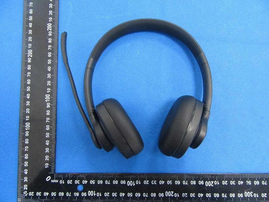
2A2F7HST-280
Jan 02, 2023HST-28X
Equipment Class
DSS - Part 15 Spread Spectrum Transmitter