2AAGMCA410ALTE module
Sequans Communications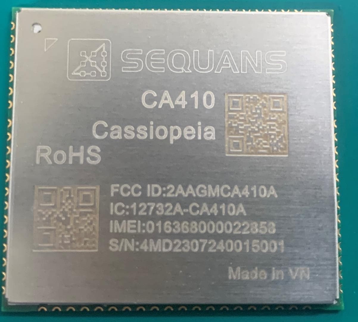
Click to zoom
Application Details
- Equipment Class
- PCB - PCS Licensed Transmitter
- Date of Grant
- Nov 19, 2023
- Application Purpose
- Original Equipment
- Date of Application
- Nov 15, 2023
- Equipment Note
- LTE module
- Frequency Range
- 788.00000000 - 798.00000000
- Company
- Sequans Communications
- Country
- United States
Documents & Files
Document Text
Text extracted from the exhibit documents filed with the FCC. Open a document above to read the original.
Users Manual
Data Sheet SEQUANS Communications 15-55 Boulevard Charles de Gaulle 92700 Colombes, France Phone. +33.1.70.72.16.00 Fax. +33.1.70.72.16.09 www.sequans.com [email protected] CA410 Module About this Data Sheet Purpose and Scope The CA410 is a complete LTE module including baseband, RF and memory, designed for CAT-4 devices. This document provides technical information about the CA410 module. The CA410 is based on Sequans’s Cassiopeia platform. Who Should Read this Data Sheet? This document is intended for engineers who are developing User Equipment (UE) for LTE systems. Changes in this Document This is the third revision of the CA410 Data Sheet. Table 1: Change History RevisionDateChanges 1June 2023N/A 2June 2023Add 1.4 MHz bandwidth for B8. New laser marking. New Chapter 5 (Regulatory). Adjust CA410 pin names in the M.2 connector pin-out table. 3August 2023Adapt the data sheet to fit the two sub-models M and L. 3aOctober 2023Add reference power figures per band in the FCC/ISED regulatory sections. i CA410 Data Sheet Rev. 3a References [1]Core technology specifications: • 3GPP E-UTRA 21 series Release 9 (EPS) • 3GPP E-UTRA 22 series Release 9 (IMEI) • 3GPP E-UTRA 23 series Release 9 (NAS, SMS) • 3GPP E-UTRA 24 series Release 9 (NAS) • 3GPP E-UTRA 31 series Release 9 (UICC) • 3GPP E-UTRA 33 series Release 9 (security) • 3GPP E-UTRA 36 series Release 9 (RAN) • 3GPP2 C.S0015-A v1.0 (SMS) • IETF, RFC 3261, 4861, 4862, 6434 For more information, consult: • ftp://ftp.3gpp.org/Specs/latest/Rel-9/21_series/ • ftp://ftp.3gpp.org/Specs/latest/Rel-9/22_series/ • ftp://ftp.3gpp.org/Specs/latest/Rel-9/23_series/ • ftp://ftp.3gpp.org/Specs/latest/Rel-9/24_series/ • ftp://ftp.3gpp.org/Specs/latest/Rel-9/31_series/ • ftp://ftp.3gpp.org/Specs/latest/Rel-9/33_series/ • ftp://ftp.3gpp.org/Specs/latest/Rel-9/36_series/ • http://www.3gpp2.org/public_html/specs/CS0015-0.pdf • https://tools.ietf.org/html/ [2] • Test specifications: 3GPP E-UTRA 36 series Release 10 (RAN): ftp:// ftp.3gpp.org/Specs/latest/Rel-10/36_series [3]Vocabulary reference: • 3GPP TR 21.905: "Vocabulary for 3GPP Specifications" For more information, see http://www.3gpp.org/ftp/specs/ archive/21_series/21.905/ [4] • "Universal Serial Bus Specification", Revision 2.0, April 27, 2000 (http:// www.usb.org/developers/docs/). ECM (Ethernet Networking Control Model) is specified in “USB Class Definitions for Communication Devices”, Version 1.1, January 19,1999, section 3.3.2. EEM (CDC Ethernet Emulation Model) is specified in “Universal Serial Bus Communications Class Subclass Specification for Ethernet Emulation Model Devices”, Revision 1.0, February 2, 2005. ii CA410 Data Sheet Rev. 3a Table of Contents Chapter 1: Product Summary......................................................................... 1 Chapter 2: Interfaces......................................................................................5 2.1 Interfaces Description for M.2 Model........................................................................................5 2.1.1 Pin Assignment............................................................................................................5 2.1.2 Pin Description............................................................................................................ 6 2.1.3 Antennas.......................................................................................................................8 2.1.4 Power......................................................................................................................... 10 2.1.5 (U)SIM....................................................................................................................... 10 2.1.6 USB............................................................................................................................10 2.1.7 UART......................................................................................................................... 10 2.1.8 Non Interfacing Signals.............................................................................................11 2.2 Interfaces Description for the LCC Model.............................................................................. 12 2.3 Digital I/O Characteristics........................................................................................................12 Chapter 3: Reliability and Radio performance..............................................15 3.1 Reliability Figures.................................................................................................................... 15 3.2 RF Performance........................................................................................................................ 16 3.3 Power Consumption..................................................................................................................16 Chapter 4: Mechanical Characteristics..........................................................17 4.1 Device Marking........................................................................................................................ 17 4.2 M.2 Device............................................................................................................................... 18 4.3 LCC Device.............................................................................................................................. 20 Chapter 5: Regulatory Approval................................................................... 21 5.1 FCC Regulatory Approval........................................................................................................21 5.2 ISED Regulatory Approval...................................................................................................... 23 Appendix A: Acronyms...................................................................................25 1 Product Summary 1.1General Description The CA410 is a complete LTE module including base-band, RF and memory. This…
Text truncated - open the document above for the full version.
Users Manual
Interfaces Interfaces Description for M.2 Model Figure 2: Position of the connectors on the M.2 board (in mm) The dimensions (in mm) of the RF connector (Foxconn™ KK12011-02-7H) is given below: Figure 3: RF Connector details 9 CA410 Data Sheet Rev. 3a Interfaces Interfaces Description for M.2 Model 2.1.4Power Table 5: Power Pads Operational Values Max Value PinNameSupplyDir.Min Value Typical Operational Value 3GPP RF Compliant Functional 5 2, 4, 70, 72, 74 VBATN/AIn3.2 V3.3 V4.4 V4.6 V 1.8 V1.62 V1.8 V1.98 V 36 SIM_VCC 4 3.0 V Out 2.7 V3.0 V3.3 V 2.1.5(U)SIM Table 6: (U)SIM Signals PinNameSupplyDirection 30SIM_RST1.8 V/3.0 VOut 32SIM_CLK1.8 V/3.0 VOut 34SIM_IO1.8 V/3.0 VIn/Out 36 SIM_VCC 6 1.8 V/3.0 VOut 66 SIM_DETECT 7 1.8 VIn 2.1.6USB Table 7: USB Signals PinNameSupplyDirection 7USB_D+3.3 VIn/Out 9USB_D-3.3 VIn/Out 2.1.7UART Table 8: UART Signals PinNameSupplyDirectionPad type 8 Reset State 63UART0_SOUT1.8 VOutBIDIR_PUOUTPUT 65UART0_SIN1.8 VOutBIDIR_PUINPUT 4 See also Section (U)SIM. 5 Functional behavior of the module with possible degradation of RF performances. 6 See range of values in Table 5. 7 SIM_DETECT is active HIGH (HIGH when a card is present, LOW when no card is present) 8 UART pad types are BIDIR_PU as detailed in Table 12. All their electrical characteristics are detailed in Table 13. 10 CA410 Data Sheet Rev. 3a Interfaces Interfaces Description for M.2 Model 2.1.8Non Interfacing Signals Table 9: Non Interfacing Signals PinNameSupplyDirectionPin Type 9 Output Class Reset State Default Setting 6MODULE_PWR_ENVDD_PWR_EN (see Table 11) InN/AN/AN/AN/A 10NETWORK_LED_N1.8 VOutBIDIR_PU4 mAINPUTINPUT, PULL-UP 23WAKE_ON_WAN_N (see below) 1.8 VOutSee belowN/AN/AN/A 67RESET_N (see below)1.8 VInN/AN/AN/AN/A RESET_N Active low (RESET). This signal is used to reset the module. The following timing requirement applies to the signals VBAT1, MODULE_PWR_EN and RESET_N. It must be respected for proper module behaviour. ts₁ ts Cold start VBAT1 MODULE_PWR_EN RESET_N Figure 4: VBAT1, MODULE_PWR_EN and RESET_N Signals Timing Requirement for Cold Start ts₁ Warm start RESET_N VBAT1 MODULE_PWR_EN Figure 5: VBAT1, MODULE_PWR_EN and RESET_N Signals Timing Requirement for Warm Start th₁ Reset cycle VBAT1 MODULE_PWR_EN RESET_N Figure 6: VBAT1, MODULE_PWR_EN and RESET_N Signals Timing Requirement for Reset Cycle Minimum values are listed in Table 10 9 Pad types are detailed in Table 12. All their electrical characteristics are detailed in Table 13. 11 CA410 Data Sheet Rev. 3a Interfaces Interfaces Description for the LCC Model Table 10: VBAT1, MODULE_PWR_EN and RESET_N Timing Values SymbolDescriptionMinimum DurationMaximum Duration tsVBAT1 setup time0 ms- ts1RESET_N setup time 1 ms- th1RESET_N hold time1 μs- WAKE_ON_WAN_N Open drain, active low. This pad wakes up the host. Requires a 10 kΩ pull-up resistor on host side. If unused, do not connect. If the host does support USB suspend-resume but not remote wake-up function, the WoWWAN# M.2 signal is needed to wake up the host. Table 11: DC Characteristics for MODULE_PWR_EN, Voltage VDD_PWR_EN ParameterMin.Nom.Max.Unit V IL Input Low Voltage -0.30.4V V IH Input High Voltage 1.1VBATV 2.2Interfaces Description for the LCC Model Data for the LCC model will be provided in a future edition of this document. 2.3Digital I/O Characteristics The voltage and current characteristics of the various I/O pads of the CA410 are given in the tables below. Table 12 details the various pad types listed in CA410 signals list. Table 12: Pad Types Detail Pad TypeDescriptionMaximum Input High Voltage AnalogueAnalogue (or power for powers and ground for grounds) Not Applicable BIDIR_PD1.8 V in/out with software controlled internal pull- down. Refer to Table 13 for DC I/O characteristics. V IH max = 3.6 V BIDIR_PU1.8 V in/out with software controlled internal pull- up. Refer to Table 13 for DC I/O characteristics. V IH max = 3.6 V IN1.8V input.V IH max = 3.6 V 12 CA410 Data Sheet Rev. 3a Interfaces Digital I/O Characteristics Pad TypeDescriptionMaximum Input High Voltage IN_PD1.8 V input with software controlled internal pull- down. Refer to Table 13 for DC I/O characteristics. V IH max = 3.6 V IN_PU1.8V input with software controlled internal pull-up.V IH max = 3.6 V OUT1.8 V output. Refer to Table 13 for DC I/O characteristics. V IH max = 3.6 V Refer to CA410 pin list for the type of I/O pad used on every termination. • The Minimum values for I OL and I OH should not be exceeded to guarantee that the logical level are not spoiled for each pad type. • The Nominal values for I OL and I OH represent the nominal values for the pad type. They are provided for information only. • The Maximum values for I OL and I OH represent the maximal values for the pad type. They are provided for information only. Table 13: DC Characteristics for Digital I/Os, Voltage 1.8 V ParameterDrive StrengthMin.Nom.Max.Unit V IL Input Low Voltage -0.30.63V V IH Input High Voltage 1.173.6V V T Threshold Point 0.790.870.94V V T+ Schmitt Trigger Low to High Threshold Point 11.121.22V V T- Schmitt Trigger High to Low Threshold Point 0.610.710.8V V T PU Threshold Point with Pull-up Resistor Enabled 0.790.860.93V V T PD Threshold Point with Pull-down Resistor Enabled 0.80.870.95V V T+ PU Schmitt Trigger Low to High Threshold Point with Pull-up Resistor Enabled 11.121.21V V T- PU Schmitt Trigger High to Low Threshold Point with Pull-up Resistor Enabled 0.610.70.8V V T+ PD Schmitt Trigger Low to High Threshold Point with Pull-down Resistor Enabled 1.011.131.23V 13 CA410 Data Sheet Rev. 3a Interfaces Digital I/O Characteristics ParameterDrive StrengthMin.Nom.Max.Unit V T- PD Schmitt Trigger High to Low Threshold Point with Pull-down Resistor Enabled 0.620.720.81V I I Input Leakage Current @ VI=1.8V or 0V ±10μA I OZ Tri-state Output Leakage Current @ VO=1.8V or 0V ±10μA Input Capacitance 3pF R PU Pull-up Resistor 5689148kΩ R PD Pull-down Resistor 5290167kΩ V OL Output Low Voltage 0.45V V OH Output High Voltage 1.35V 2…
Text truncated - open the document above for the full version.
Users Manual
5 Regulatory Approval Band B8 and CBRS band (B48) approval is only relevant under FCC jurisdiction. 5.1FCC Regulatory Approval FCC-ID: 2AAGMCA410A (single modular approval) This above identified LTE radio module is not intended to be provided to end-users but is for installation by OEM integrators only. Installation/Integration OEM integrators must follow Sequans’ installation instructions to provide for and benefit from FCC compliant module integrations and must abide especially by the following provisions: The maximum antenna gain values (accounting for cable attenuation) to comply with the FCC maximum ERP/EIRP limits and with RF Exposure rules: • LTE band 2 (1850-1910 MHz): 9.26 dBi • LTE band 4 (1710-1755 MHz): 6.66 dBi • LTE band 5 (824-849 MHz): 10.89 dBi • LTE band 8 (897.5-900.5 MHz): 10.86 dBi • LTE band 12 (699-716 MHz): 13.58 dBi • LTE band 13 (777-787 MHz): 10.33 dBi • LTE band 14 (788-798): 10.32 dBi • LTE band 26 (814-849): 10.84 dBi • LTE band 48 (3550-3700): 1.24 dBi • LTE band 66 (AWS-3): 6.66 dBi Sequans's module integration guidelines must be closely followed. Compliance of host integrations of the module is limited to hosts adaptation designs which are identical to Sequans' reference design. Host integrations with adaption designs deviating from Sequans' reference design require either class 2 permissive change to this modular approval or a separate host approval with different FCC-ID; Host integrations with co-located (simultaneously operating) radio transmitters must be evaluated in accordance with FCC multi-transmitter rules and may require either class 2 permissive change to this modular approval or a separate host approval with different FCC-ID, dependent on the result of the evaluation; Inquiry at FCC or a TCB is urgently recommended. Integrations of the module into host products which are intended for portable use, i.e. less than 20cm distance between its radiating structures (antenna) and the body of nearby persons, or which otherwise put additional technical requirements like Hearing Aid compatibility require either class 2 permissive change to this modular approval or a separate host approval with different FCC-ID; Compliance with Unwanted Emission Limits for Digital Device 21 CA410 Data Sheet Rev. 3a Regulatory Approval FCC Regulatory Approval If the OEM host integration fully complies with the above described reference design and can completely inherit and rest on compliance of the existing modular approval the OEM remains still responsible to show compliance of the overall end-product with the FCC limits for unwanted conducted and radiated emissions from the digital device (unintentional radio) portion of such end-product (commonly addressed as part 15B compliance or similar). End-product Labelling • The module's FCC-ID must either be visible from the exterior of the host product (e.g. per window) or per electronic display, or shall be displayed on an additional exterior label per the following or similar string: contains FCC-ID: 2AAGMCA410A • Digital Device - Unwanted Emissions Notice: If the end-product falls under part 15 of the FCC rules (it shall display the following user notice on its exterior acc. to part 15.19 (the notice may be printed in the manual in case the host is too small): This device complies with Part 15 of the FCC Rules. Operation is subject to the following two conditions: (1) This device may not cause harmful interference, and (2) This device must accept any interference received, including interference that may cause undesired operation. • Further Labelling Requirements may apply dependent on the FCC rule parts relevant to the host product. • End-product User Instructions / Notices in the Manual: At a minimum, end-product users must be provided with the following notices at a prominent location of the product literature furnished with the product: – Product Modifications: Modifications not expressly approved by the party responsible for compliance could void the user’s authority to operate this equipment. – RF Exposure Compliance: This equipment complies with FCC radio frequency radiation exposure rules and limits set forth for an uncontrolled environment, when installed and operated with minimum distance of 20 cm between its radiating structures (antenna) and the body of nearby persons and when not operated simultaneously with other nearby radio-transmitters. – Maximum Antenna Gain: The user instructions of end-products equipped with standard external antenna connectors for the modular radio transmitter providing the option to connect other antennae than those which may or may not be bundled with the end-product must list the maximum allowed antenna gain values as derived from those given above, accounting for the cable attenuations of the actual installation. – Digital Device - Unwanted Emissions Notice: If the end-product is or contains a digital device (unintentional radio portions) and is not exempted by its use case (like vehicular use) the following part 15.105 (b) user notice shall be provided at prominent location of the product literature: This equipment has been tested and found to comply with the limits for a Class B digital device, pursuant to part 15 of the FCC rules. These limits are designed to provide reasonable protection against harmful interference in a residential installation. This equipment generates, uses and can radiate radio frequency energy and, if not installed and used in accordance with the instructions, may cause harmful interference to radio communications. However, there is no guarantee that interference will not occur in a particular installation. If this equipment does cause harmful interference to radio or television reception, which can be determined by turning the equipment off and on, the user is 22 CA410 Data Sheet Rev. 3a Regulatory Approval ISED Regulatory Approval encouraged to try to correct the interference by one or more of the following measures: ◦Reorient or relocate the receiving ant…
Text truncated - open the document above for the full version.
Attestation Statements
Certification designating a U.S. agent for service of process. (as required by section 2.911(d) (7)) Date: 02/10/2023 Federal Communications Commission Equipment Authorization Branch 7435 Oakland Mills Rd. Columbia MD 21046 FCC ID: 2AAGMCA410A To whom it may concern: We, Sequans Communications 90 Washington Valley Rd, Bedminster, New Jersey, 7921, USA FRN: 0034219402 hereby certify that the following company, Sequans Communications 90 Washington Valley Rd, Bedminster, New Jersey, 7921, USA FRN: 0034219402 is our designated U.S. agent for service of process and we acknowledge: •our consent to accept service of process in the United States for matters related to the applicable equipment at the physical U.S. address and email address of the designated U.S. agent •the acceptance to maintain an U.S. agent for no less than one year after the grantee has terminated all marketing and importation or the conclusion of any Commission-related proceeding involving the equipment. Sincerely, By: Sunpreet Kaur Title: NAM & EMEA Certifications Manager Telephone: +1.206.248.6609 email: [email protected] We Sequans Communications acknowledge our obligation to accept service of process in the United States for matters related to the applicable equipment at our physical U.S. address and email address stated above. Sincerely, By: Sunpreet Kaur Title: NAM & EMEA Certifications Manager Telephone: +1.206.248.6609 email: [email protected]
Attestation Statements
Date: 02/10/2023 Federal Communications Commission Equipment Authorization Branch 7435 Oakland Mills Rd. Columbia MD 21046 FCC ID: 2AAGMCA410A To whom it may concern: We, Sequans Communications 90 Washington Valley Rd, Bedminster, New Jersey, 7921, USA Hereby certify that, •the equipment for which authorization is sought is not “covered” equipment prohibited from receiving an equipment authorization pursuant to section 2.903 of the FCC rules. •as of the date of the filing of the application, the applicant is not identified on the Covered List as an entity producing “covered” equipment. Sincerely, ________________________________________ By: Sunpreet Kaur Title: NAM & EMEA Certification Manager Telephone: +12062476609 email: [email protected]
Cover Letter(s)
Date: 02/10/2023 Federal Communications Commission Equipment Authorization Branch 7435 Oakland Mills Rd. Columbia MD 21046 FCC ID: 2AAGMCA410A To whom it may concern: We, Sequans Communications 90 Washington Valley Rd, Bedminster, New Jersey, 7921, USA hereby authorize, DEKRA Testing and Certification S.A.U. Parque Tecnológico de Andalucía C/Severo Ochoa, 2 & 6 | 29590 | Málaga | Spain Agent: Álvaro Corrales Sedeño e-mail:[email protected] Phone:+34 952 619 198 to act as our agent in the preparation of this application for equipment certification, including the signing of all documents relating to these matters. We also hereby certify that neither we nor any party to this application are subject to a denial of U.S. Federal benefits, which include FCC benefits, pursuant to Section 5301 of the Anti-Drug Abuse Act of 1988, U.S.C. 862 because of conviction for possession or distribution of controlled substance. For instances where our authorized agent signs the application for certification on our behalf, I acknowledge that all responsibility for complying with the terms and conditions for Certification, as specified by DEKRA Testing and Certification, S.A.U., still resides with us. This agreement expires one year from the current date. Sincerely, ________________________________________ By: Sunpreet Kaur Title: NAM & EMEA Certification Manager Telephone: +12062476609 email: [email protected]
Cover Letter(s)
Date: 02/10/2023 Federal Communications Commission Equipment Authorization Branch 7435 Oakland Mills Rd. Columbia MD 21046 FCC ID: 2AAGMCA410A To whom it may concern: We, Sequans Communications 90 Washington Valley Rd, Bedminster, New Jersey, 7921, USA hereby request requests that a part of the subject FCC application be held confidential to avoid release of sensitive information of the product to the public pursuant to §0.457(d)(1)(ii) and §0.459 of the Commission’s Rules (47 C.F.R.) and §552 (b)(4) of the Freedom of Information Act, For the product stated above, we request that the following information be withheld from public disclose: Type of Confidentiality Requested Exhibit Short Term Permanent Block Diagrams Short Term Permanent Operation Description Short Term Permanent Schematics Short Term Permanent Parts List & Placement/BOM Short Term Permanent Tune-Up Procedure Short Term Permanent SDR Software and Security Information Short Term Test Setup Photos Short Term User’s Manual Short Term External Photos Short Term Internal Photos Permanent Confidentiality: The above materials contain trade secrets and proprietary information not customarily released to the public. The public disclosure of these matters might be harmful to us and provide unjustified benefits to our competitors. Short-Term Confidentiality: We hereby request short-term confidentiality for the product stated above to avoid premature release of sensitive information prior to marketing or release of the product to the public. Release date of short-term confidentiality is: 45 days from grant date marked 90 days from grant date marked 135 days from grant date marked 180 days from grant date marked Specific date: We are also aware that we are responsible to notify DEKRA Testing and Certification S.A.U. in the event information regarding the product or the product is made available to the public. DEKRA Testing and Certification S.A.U. will then release the documents listed above for public disclosure pursuant to FCC Public Notice DA 04-1705. Sincerely, ________________________________________ By: Sunpreet Kaur Title: NAM & EMEA Certification Manager Telephone: +12062476609 email: [email protected]
Cover Letter(s)
Date: 02/10/2023 Federal Communications Commission Equipment Authorization Branch 7435 Oakland Mills Rd. Columbia MD 21046 FCC ID: 2AAGMCA410A To whom it may concern: We, Sequans Communications 90 Washington Valley Rd, Bedminster, New Jersey, 7921, USA through the following attestation, hereby address the requirements to support modular approval pursuant to §15.212 of the Commission’s Rules: Modular approval requirement Yes No* (i)The radio elements of the modular transmitter must have their own shielding. The physical crystal and tuning capacitors may be located external to the shielded radio elements. X (ii)The modular transmitter must have buffered modulation/data inputs (if such inputs are provided) to ensure that the module will comply with part 15 requirements under conditions of excessive data rates or over-modulation. X (iii)The modular transmitter must have its own power supply regulation.X (iv)The modular transmitter must comply with the antenna and transmission system requirements of §§15.203, 15.204(b) and 15.204(c). The antenna must either be permanently attached or employ a “unique” antenna coupler (at all connections between the module and the antenna, including the cable). The “professional installation” provision of §15.203 is not applicable to modules but can apply to limited modular approvals under paragraph (b) of this section. X (v)The modular transmitter must be tested in a stand-alone configuration, i.e., the module must not be inside another device during testing for compliance with part 15 requirements. Unless the transmitter module will be battery powered, it must comply with the AC line conducted requirements found in §15.207. AC or DC power lines and data input/output lines connected to the module must not contain ferrites, unless they will be marketed with the module (see §15.27(a)). The length of these lines shall be the length typical of actual use or, if that length is unknown, at least 10 centimeters to ensure that there is no coupling between the case of the module and supporting equipment. Any accessories, peripherals, or support equipment X connected to the module during testing shall be unmodified and commercially available (see §15.31(i)). (vi) The modular transmitter must be equipped with either a permanently affixed label or must be capable of electronically displaying its FCC identification number. X (vii) The modular transmitter must comply with any specific rules or operating requirements that ordinarily apply to a complete transmitter and the manufacturer must provide adequate instructions along with the module to explain any such requirements. A copy of these instructions must be included in the application for equipment authorization. X (viii) The modular transmitter must comply with any applicable RF exposure requirements in its final configuration. X * Shall provide a detailed explanation if the answer is “No”. Sincerely, ________________________________________ By: Sunpreet Kaur Title: NAM & EMEA Certification Manager Telephone: +12062476609 email: [email protected]
Cover Letter(s)
Date: 02/10/2023 Federal Communications Commission Equipment Authorization Branch 7435 Oakland Mills Rd. Columbia MD 21046 FCC ID: 2AAGMCA410A To whom it may concern: We, Sequans Communications 90 Washington Valley Rd, Bedminster, New Jersey, 7921, USA through the following attestation, hereby address the fourth requirement to support modular approval. •This device is designed for mobile or fixed operation; portable operation is subject to a Class 2 permissive change application or to a new and separate FCC ID. •The maximum antenna gain is limited to those calculated in the RF exposure exhibit. •The product has an FCC ID label on the device itself. Also, the OEM host product manufacturer will be informed to display a label referring to the enclosed module. •We request to include in the grant the following words in the device description or grant notes: “modular transmitter” or “transmitter module”. If there are any additional questions or if further information is needed, please contact us. Sincerely, ________________________________________ By: Sunpreet Kaur Title: NAM & EMEA Certification Manager Telephone: +12062476609 email: [email protected]
External Photos
Photographs-external
ID Label/Location Info
V All Label position T99W464.00 CA410 LCC Wendy Chang Wendy Chang Wendy Chang 00 01 N/AN/A N/AN/A2023/ 0830/ First release -- -- Allen Chang 1/500 1/1000 1/500 1/250 Carton Label Bag Label Reel Label ItemDescriptionP/NQTY 1 2 3 503.01877.005 1/1000 Pallet Label 4 5 6 503.00089.005 Carton 5.Carton Label 6.Pallet Label Vacuum-ESD Bag Foam k ml ls nq lor mps PKYMDSSSSS 1.Panel label 2.Tray label Baking Tray*10pcs Reel 3.Reel label Vacuum-ESD Bag 4.Bag label 4.Bag label Module ESD bag after vacuum picture for reference. Stick bag label on vacuum-ESD bag . Stick Tray Label on Baking tray Stick Panel Label on Panel 1 pile Baking tray use 1pc Tray Label 1 pile = 10pcs Baking trays = 250 pcs Modules 503.00039.055 503.00039.055 1/9 Panel Label Tray Label 503.00098.005 503.00098.005 2023/06/19 Update content for DVT RoHS FCC ID:2AAGMCA410A IMEI:XXXXXXXXXXXXXXX IC:12732A-CA410A S/N:VVVYYMMDDLLLLSSS CA410 Cassiopeia Made in VN CA410 LCC Panel Label V T99W464.00 Wendy Chang Wendy Chang Wendy Chang 00 01N/AN/A N/AN/AFirst release -- Allen Chang 2023/06/19 P: PCB la bel Z: Foxconn lo ca�on YMD: Year , month, day LLLL: serial number (0001~9999) Bar code: 128 code, 2.54mm heig ht Font: Verdana, Bold,2pt 503.00039.055 (19.05*5mm) Panel label PZYMDLLLL 2023/08/30Update content for DVT 503.00039.055 CA410 LCC 2023/08/30 Laser V T99W464.00 Wendy Chang Wendy Chang Wendy Chang 00 01N/AN/A N/AN/AFirst release -- Allen Chang 2023/06/19 Update content for DVT SCALE:1:1 SCALE:2:1 RoHS FCC ID:2AAGMCA410A IMEI:XXXXXXXXXXXXXXX IC:12732A-CA410A S/N:VVVYYMMDDLLLLSSS CA410 Cassiopeia 29 32 29 32 Made in VN RoHS FCC ID:2AAGMCA410A IMEI:XXXXXXXXXXXXXXX IC:12732A-CA410A S/N:VVVYYMMDDLLLLSSS CA410 Cassiopeia Made in VN 1 2 6 7 8 9 11 10 5 4 3 2 2 No. ① ② ③ ④ ⑤ ⑥ Name Customer Logo Model Name Pla tform Name Compliance Logo IMEI 2D Barcode SN 2D Barcode Content CA410 Cassio peia RoHs Siz e Character:2*16mm Icon:4*4mm Aria l Regula r 6.5pt (Heig h…
Text truncated - open the document above for the full version.
Contact Information
Applicant
Sunpreet Kaur(Certification Manager)
Technical Contact
Sequans CommunicationsSunpreet Kaur
[email protected]1 206 248 6609
90 Washington Valley Road Bedminster New Jersey · United States
Non-Technical Contact
Sequans CommunicationsSunpreet Kaur
[email protected]1 206 248 6609
Test Firm
DEKRA Testing and Certification, S.A.U.Rafael Lopez Martin
Technical Specifications
| # | Rule Parts | Frequency Range | Power Output | Emission | Tolerance |
|---|---|---|---|---|---|
| 18 | 9 | 788 MHz - 798 MHz | 200.00 mW | 9M12D7W | 0.01 ppm |
Other Applications from Sequans Communications
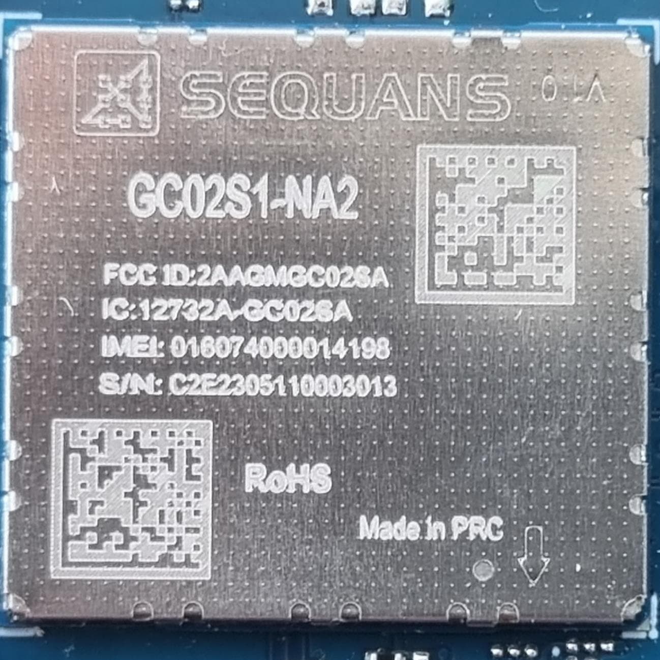
2AAGMGC02SA
Dec 12, 2023LTE Cat1-bis module
Equipment Class
CXX - Communications Rcvr for use w/ licensed Tx and CBs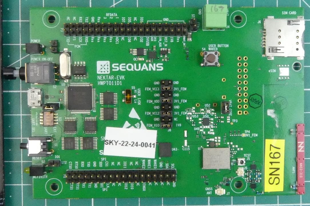
2AAGM66431
Dec 06, 2022SKY66431
Equipment Class
JAB - Part 15 Class B Digital Device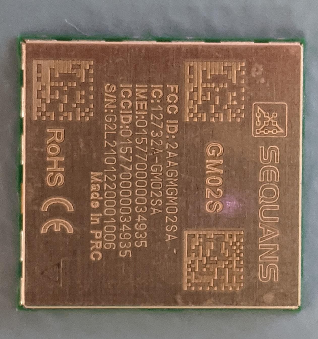
2AAGMGM02SA
Apr 15, 2021GM02S module
Equipment Class
JAB - Part 15 Class B Digital Device
2AAGMGM02S
Jan 17, 2021GM02S module
Equipment Class
PCB - PCS Licensed Transmitter
2AAGMGMQGOB
Nov 04, 2020Monarch Go-GPS BLE
Equipment Class
DTS - Digital Transmission System