2ABRU-BLEM205INBT5.0 Low Energy Module - Indutrial Grade
Guangzhou BDE Technology Inc.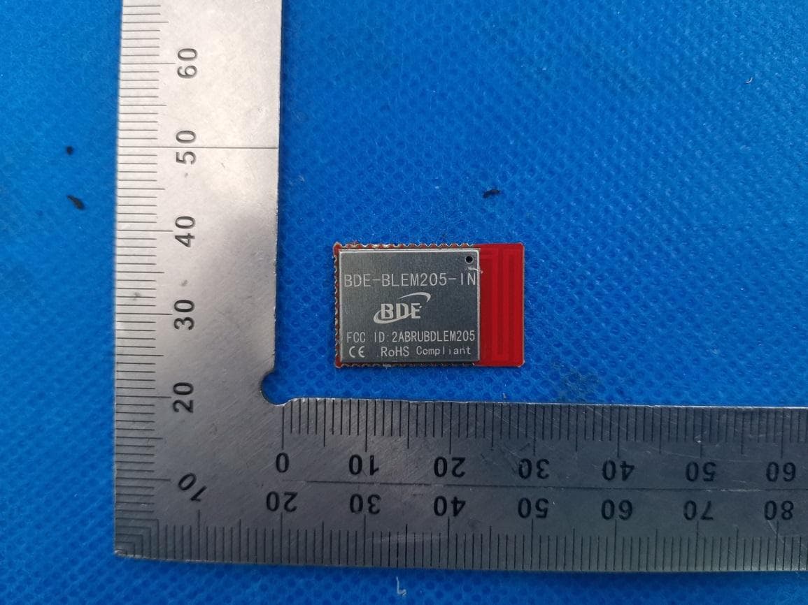
Click to zoom
Application Details
- Equipment Class
- DTS - Digital Transmission System
- Date of Grant
- Apr 15, 2021
- Application Purpose
- Original Equipment
- Date of Application
- Apr 15, 2021
- Equipment Note
- BT5.0 Low Energy Module - Indutrial Grade
- Frequency Range
- 2402.00000000 - 2480.00000000
- Country
- China
Documents & Files
Document Text
Text extracted from the exhibit documents filed with the FCC. Open a document above to read the original.
Users Manual
BDE-BLEM205-IN BDE Technology Inc. BT5.0 Low Energy Module – Industrial Grade Key Features Bluetooth 4 and 5 low energy Powerful ARM Cortex-M4F processor Clock speed: up to 48MHz 352KB of In-System programmable flash with 8KB cache 80KB SRAM 8KB of cache SRAM 2-Pin cJTAG and JTAG debugging Support Over-the-Air upgrade (OTA) Ultra-Low power sensor controller with 4KB of SRAM 31 GPIOs 4 x 32-Bit or 8 x 16-Bit general purpose timer 12-Bit ADC, 200 kSamples/s, 8 channels 2 x comparator with internal reference DAC Programmable current source 2 x UART 2 x SSI (SPI, MICROWIRE, TI) IIC, IIS Real-Time-Clock (RTC) AES 128- and 256-bit crypto accelerator ECC and RSA public key hardware accelerator SHA2 accelerator (Full suite up to SHA-512) True Random Number Generator (TRNG) Capacitive sensing, up to 8 channels Integrated temperature and battery monitor On-Chip buck DC/DC converter RF performance TX power: -21dBm to 5dBm RX sensitivity: up to -105dBm (LE coded PHY) Communication range: about 250 meters (LOS) – Long Range Mode Antenna: PCB antenna, 1.17 dBi gain Size: 22.95 mm x 15 mm x 2.1 mm (With Shielding) Ultra low power consumption: Shutdown: 120nA (Wake up on external events) Standby: 0.95uA (RTC running and RAM/CPU retention) BDE-BLEM205-IN BDE Technology Inc. RX current: 6.9mA TX current @ 0dBm: 7.4mA TX current @ 5dBm: 9.7mA Industrial grade operating temperature range from -40⁰C to +105⁰C Pin to pin compatible with BDE-BLEM205 BQB, FCC, CE, RoHS compliant Descriptions BDE-BLEM205-IN is a Bluetooth 4 and 5 single-mode compliant Bluetooth low energy module targeted at low power sensors and PC/Phone accessories. BDE-BLEM205-IN highly integrates Bluetooth Low Energy radio, stack, profile and applications in a SoC, without the need of using an external MCU. The module also offers flexible hardware interfaces for the sensor application. It enables ultra-low power connectivity and data transfer for the applications that are sensitive to power consumption, size and cost. BDE-BLEM205-IN BDE Technology Inc. Applications Medical devices Sports and fitness equipment Home electronics Mobile and PC accessories Industry automation Electrical Characteristics Absolute maximum rating Rating Min Typ Max Unit Notes Storage Temperature -40 - 125 °C VDD -0.3 - 4.1 V Other Digital Terminals -0.3 - VDDS+0.3≤4.1 V Voltage on ADC input -0.3 - VDDS V Voltage scaling enabled -0.3 - 1.49 V Voltage scaling disabled, internal reference -0.3 - VDDS/2.9 V Voltage scaling disabled, VDDS as reference RF pin - - 5 dBm Recommended operating conditions Rating Min Typ Max Unit Operating Temperature -40 - 105 °C VDD 1.8 3.3 3.8 V BDE-BLEM205-IN BDE Technology Inc. Pinout Fig. 2: The pinout of BDE-BLEM205-IN (TOP VIEW) Table 1: Pin definitions of BDE-BLEM205-IN Pin Number Pin Name Definitions 1 DIO_0 GPIO, Sensor Controller 2 DIO_1 GPIO, Sensor Controller 3 DIO_2 GPIO, Sensor Controller 4 DIO_3 GPIO, Sensor Controller 5 DIO_4 GPIO, Sensor Controller 6 DIO_5 GPIO, Sensor Controller, high-drive capability 7 DIO_6 GPIO, Sensor Controller, high-drive capability 8 DIO_7 GPIO, Sensor Controller, high-drive capability 9 GND Power Ground 10 VDD Power Supply 11 DIO_8 GPIO 12 DIO_9 GPIO 13 DIO_10 GPIO 14 DIO_11 GPIO 15 DIO_12 GPIO 16 DIO_13 GPIO 17 DIO_14 GPIO 18 DIO_15 GPIO 19 JTAG_TMS JTAG TMSC, high-drive capability 20 JTAG_TCK JTAG TCKC 21 DIO_16 GPIO, JTAG_TDO, high-drive capability BDE-BLEM205-IN BDE Technology Inc. 22 DIO_17 GPIO, JTAG_TDI, high-drive capability 23 DIO_18 GPIO 24 DIO_19 GPIO 25 DIO_20 GPIO 26 DIO_21 GPIO 27 DIO_22 GPIO 28 RESET Reset, active-low 29 DIO_23 GPIO, Sensor Controller, Analog 30 DIO_24 GPIO, Sensor Controller, Analog 31 DIO_25 GPIO, Sensor Controller, Analog 32 DIO_26 GPIO, Sensor Controller, Analog 33 DIO_27 GPIO, Sensor Controller, Analog 34 DIO_28 GPIO, Sensor Controller, Analog 35 DIO_29 GPIO, Sensor Controller, Analog 36 DIO_30 GPIO, Sensor Controller, Analog Overall Dimensions Fig. 3 shows the overall dimensions of BDE-BLEM205-IN. The module measures 22.95mm long by 15mm wide by 2.1mm high with the shield. Fig. 3: Overall Dimensions of BDE-BLEM205-IN BDE-BLEM205-IN BDE Technology Inc. Module Location In order to get a fine performance when integrate the module to your product, it is advised to use the recommended module location to the respective PCB. Location in X-Y plane Fig. 4: Recommended location in X-Y plane Fig. 5: Not recommended location in X-Y plane BDE-BLEM205-IN BDE Technology Inc. Location in Z plane Fig. 6: Recommended location in Z plane Fig. 7: Not recommended location in Z plane Typical Solder Reflow Profile Fig. 8: Typical Solder Reflow Profile BDE-BLEM205-IN BDE Technology Inc. Package Information Fig. 9: Package FCC Warning Integration instructions for host product manufacturers according to KDB 996369 D03 OEM Manual v01 1. List of applicable FCC rules FCC Part 15.247 2. Specific operational use conditions This transmitter/module and its antenna(s) must not be co-located or operating in conjunction with any transmitter. This information also extends to the host manufacturer’s instruction manual. 3. Limited module procedures Not applicable 4. Trace antenna designs It is “not applicable” as trace antenna which is not used on the module. 5. RF exposure considerations This equipment complies with FCC RF radiation exposure limits set forth for an uncontrolled environment. This compliance to FCC radiation exposure limits for an uncontrolled environment, and minimum of 20cm separation between antenna and body. The host product manufacturer would provide the above information to end users in their end-product manuals. 6. Antennas BDE-BLEM205-IN BDE Technology Inc. PCB Antenna; 1.71dBi; 2402MHz ~ 2480MHz 7. Label and compliance information The end product must carry a physical label or shall use e-labeling followed KDB784748D01 and KDB 784748 stating “Contains Transmitter Module FCC ID: 2AB…
Text truncated - open the document above for the full version.
Cover Letter(s)
Guangzhou BDE Technology Inc. B2-403, Chuangyi Building, 162 Science Avenue, Huangpu District, Guangzhou 510663, China Agent Authorization Company: Guangzhou BDE Technology Inc. Address: B2-403, Chuangyi Building, 162 Science Avenue, Huangpu District, Guangzhou 510663, China Product Name: BT5.0 Low Energy Module - Indutrial Grade Model Number(s): BDE-BLEM205-IN, BDE-BLEM205 Product Description: BT5.0 Low Energy Module - Indutrial Grade We authorize MiCOM Labs Inc., 575 Boulder Court, Pleasanton, California 94566, USA, to act on our behalf on all matters concerning the certification of above named equipment. We declare that MiCOM Labs Inc. is allowed to forward all information related to the approval and certification of equipment to the regulatory agencies as required and to discuss any issues concerning the approval application. Any and all acts carried out by MiCOM Labs on our behalf shall have the same effect as acts of our own. Signature: Date: Mar. 19, 2021 Name: Jacky Tian Title: General Manager Company: Guangzhou BDE Technology Inc.
Cover Letter(s)
Guangzhou BDE Technology Inc. B2-403, Chuangyi Building, 162 Science Avenue, Huangpu District, Guangzhou 510663, China Office of Engineering Technology Federal Communications Commission 7435 Oakland Mills Road Columbia, MD 21046 USA Date: Mar. 19, 2021 Subject; Request for Confidentiality FCC ID: 2ABRU-BLEM205IN To Whom It May Concern, Pursuant to the provisions of the Commission’s rules Title 47 Sections §0.457 and §0.459, we are requesting the Commission to withhold the following attachment(s) as confidential documents from public disclosure indefinitely. These documents contain detailed system and equipment descriptions and are considered as proprietary information in operation of the equipment. The public disclosure of these documents might be harmful to our company and would give competitors an unfair advantage in the market. Schematic Diagram Block Diagram Operational Description Parts List Tune -up Procedure It is our understanding that all measurement test reports, FCC ID label format and correspondence during the certification review process cannot be granted as confidential documents and this information will be available for public review once the grant of equipment authorization is issued. Sincerely, Signature: Name: Jacky Tian Title: General Manager
Cover Letter(s)
Guangzhou BDE Technology Inc. B2-403, Chuangyi Building, 162 Science Avenue, Huangpu District, Guangzhou 510663, China Mar. 19, 2021 Office of Engineering Technology Federal Communications Commission 7435 Oakland Mills Road Columbia, MD 21046 USA Subject: Explanation of differences between product types FCC ID: 2ABRU-BLEM205IN Models: BDE-BLEM205-IN, BDE-BLEM205 To Whom It May Concern: We, The Guangzhou BDE Technology Inc. hereby declare that the model : BDE- BLEM205-IN is identical with the model : BDE-BLEM205, except the model name. BDE-BLEM205-IN can operate from -40°C to 105°C, while BDE-BLEM205 operates from -40°C to 85°C Except for the different above, no other modification is performed. Sincerely, Guangzhou BDE Technology Inc. Signature: [Jacky Tian, General Manager]
Cover Letter(s)
Guangzhou BDE Technology Inc. B2-403, Chuangyi Building, 162 Science Avenue, Huangpu District, Guangzhou 510663, China RE FCC ID: 2ABRU-BLEM205IN To the certification reviewer: We are hereby applying for [full] modular approval of the above-referenced FCC ID, based on compliance with [all] of the criteria as detailed below. Sincerely, [Jacky Tian] [General Manager] Part 15 Unlicensed Single Modular Transmitter Approval Justification per 15.212 Requirement per 15.212 reference (i) The radio elements of the modular transmitter must have their own RF shielding. Shielding is provided by a metal cover over the circuitry. (ii) The modular transmitter must have buffered modulation/data inputs (if such inputs are provided. All modulation and data inputs are buffered by circuitry on the transmitter chip. (iii) The modular transmitter must have its own power supply regulation. Power supply regulation is provided by circuitry on the transmitter chip. (iv) The modular transmitter must comply with the antenna and transmission system requirements of §§ 15.203, 15.204(b) and 15.204(c). The antenna is fixed. (v) The modular transmitter must be tested in a stand-alone configuration, i.e., the module must not be inside another device during testing for compliance with Part 15 parameters. Testing was performed in a stand-alone configuration as shown in the test setup photos. Guangzhou BDE Technology Inc. B2-403, Chuangyi Building, 162 Science Avenue, Huangpu District, Guangzhou 510663, China (vi) The modular transmitter must be equipped with either a permanently affixed label or must be capable of electronically displaying its FCC identification number. If the FCC ID is not visible when the module is installed inside another device, then the outside of the device into which the module is installed must also display a label referring to the enclosed module. The modular was labeled with its own FCC ID. The outside of device in to which the module is installed will labeled Contains TX FCC ID: 2ABRU- BLEM205IN, Please refer to User Manual. (vii) The modular transmitter must comply with any specific rules or operating requirements that ordinarily apply to a complete transmitter and the manufacturer must provide adequate instructions along with the module to explain any such requirements. A copy of these instructions must be included in the application for equipment authorization. The modular is comply with all applicable FCC rules. Any modifications, not expressly approved by the manufacturer could void the authority to operate in these regions. (viii) The modular transmitter must comply with any applicable RF exposure requirements in its final configuration. This module operates under Part 15 .247 which is exempt from RF exposure evaluation owing to the very low operating power.
External Photos
External Photos TOP VIEW OF EUT BOTTOM VIEW OF EUT FRONT VIEW OF EUT BACK VIEW OF EUT LEFT VIEW OF EUT RIGHT VIEW OF EUT
ID Label/Location Info
FCC ID and IC Label Location 10mm*8mm 10mm*8mm FCC ID: 2ABRU-BLEM205IN IC: 25657-BLEM205 BDE-BLEM205
Internal Photos
Internal Photos INTERNAL VIEW-1 OF EUT INTERNAL VIEW-2 OF EUT Antenna INTERNAL VIEW-3 OF EUT
RF Exposure Info
RF EXPOSURE EVALUATION 1. PRODUCT INFORMATION Product Description BT5.0 Low Energy Module - Indutrial Grade Model Name BDE-BLEM205-IN FCC ID 2ABRU-BLEM205IN 2. EVALUATION METHOD AND LIMIT Human exposure to RF emissions from mobile devices (47 CFR §2.1091) may be evaluated based on the MPE limits adopted by the FCC for electric and magnetic field strength and/or power density, as appropriate, since exposures are assumed to occur at distances of 20 cm or more from persons. LIMITS FOR GENERAL POPULATION / UNCONTROLLED EXPOSURE Frequency Range (MHz) E-field Strength (E) (V/m) Magnetic Field Strength (H) (A/m) Power Density (S) (mW/cm 2 ) Averaging Time |E| 2 , |H| 2 or S (Minutes) 0.3 -- 1.34 614 1.63 (100)* 30 1.34 -- 30 824/f 2.19/f (180/f 2 )* 30 30 -- 300 27.5 0.073 0.2 30 300 -- 1500 -- -- f/1500 30 1500 -- 100,000 -- -- 1.0 30 *Note: 1. f= Frequency in MHz * Plane-wave Equivalent Power Density 2. The averaging time for General Population/Uncontrolled exposure to fixed transmitters is not applicable for mobile and portable transmitters. See 47 CFR §§2.1091 and 2.1093 on source-based time-averaging requirement for mobile and portable transmitters. S=PG/4πR² Where: S=power density P=power input to antenna G=power gain of the antenna in the direction of interest relative to an isotropic radiator R=distance to the center of radiation of the antenna CALCULATION A minimum test separation distance ≥ 20 cm is required between the antenna and radiating structures of the device and nearby persons to apply mobile device exposure limits. The distance must be at least 20 cm and fully supported by the operating and installation configurations of the transmitter and its antenna(s), according to the source-based time-averaged maximum power requirements of § 2.1091(d)(2). In cases where cable losses or other attenuations are applied to determine compliance, the most conservative operating configurations and exposure conditions must be evaluated. BT Antenna Gain=2.18dBi (Numeric 1.65), π=3.14 Note: 1. Only the worst case recorded. 2.conclusion Compliance the RF exposure requirement Frequency Output Power Output Power Power Density Power Density Limit MHz dBm mW mW/cm 2 mW/cm 2 2440(125KHz) 4.540 2.84 0.000934 1 2440(500KHz) 4.547 2.85 0.000936 1 2480(1M) 4.425 2.77 0.000909 1 2440(2M) 4.523 2.83 0.000929 1
Test Report
Page 1 of 100 FCC Test Report Report No.: AGC02390201206FE02 FCC ID : 2ABRU-BLEM205IN APPLICATION PURPOSE : Original Equipment PRODUCT DESIGNATION : BT5.0 Low Energy Module - Indutrial Grade BRAND NAME : BDE MODEL NAME : BDE-BLEM205-IN, BDE-BLEM205 APPLICANT : Guangzhou BDE Technology Inc. DATE OF ISSUE : Feb. 06, 2021 STANDARD(S) : FCC Part 15.247 REPORT VERSION : V1.0 Attestation of Global Compliance (Shenzhen) Co., Ltd Report No.: AGC02390201206FE02 Page 2 of 100 REPORT REVISE RECORD Report Version Revise Time Issued Date Valid Version Notes V1.0 / Feb. 06, 2021 Valid Initial Release Report No.: AGC02390201206FE02 Page 3 of 100 TABLE OF CONTENTS 1. VERIFICATION OF COMPLIANCE .................................................................................................................. 5 2. GENERAL INFORMATION .............................................................................................................................. 6 2.1. PRODUCT DESCRIPTION ........................................................................................................................ 6 2.2. TABLE OF CARRIER FREQUENCYS ....................................................................................................... 6 2.3. RELATED SUBMITTAL(S)/GRANT(S) ....................................................................................................... 7 2.4. TEST METHODOLOGY ............................................................................................................................. 7 2.5. SPECIAL ACCESSORIES .......................................................................................................................... 7 2.6. EQUIPMENT MODIFICATIONS ................................................................................................................. 7 2.7. ANTENNA REQUIREMENT ....................................................................................................................... 7 3. MEASUREMENT UNCERTAINTY ................................................................................................................... 8 4. DESCRIPTION OF TEST MODES ................................................................................................................... 9 5. SYSTEM TEST CONFIGURATION ................................................................................................................ 10 5.1. CONFIGURATION OF TESTED SYSTEM ............................................................................................... 10 5.2. EQUIPMENT USED IN TESTED SYSTEM .............................................................................................. 10 5.3. SUMMARY OF TEST RESULTS .............................................................................................................. 10 6. TEST FACILITY .............................................................................................................................................. 11 7. PEAK OUTPUT POWER ................................................................................................................................ 12 7.1. MEASUREMENT PROCEDURE .............................................................................................................. 12 7.2. TEST SET-UP (BLOCK DIAGRAM OF CONFIGURATION) .................................................................... 12 7.3. LIMITS AND MEASUREMENT RESULT .................................................................................................. 13 8. 6 DB BANDWIDTH ......................................................................................................................................... 19 8.1. MEASUREMENT PROCEDURE .............................................................................................................. 21 8.2. TEST SET-UP (BLOCK DIAGRAM OF CONFIGURATION) .................................................................... 21 8.3. LIMITS AND MEASUREMENT RESULTS ............................................................................................... 21 9. CONDUCTED SPURIOUS EMISSION........................................................................................................... 29 9.1. MEASUREMENT PROCEDURE .............................................................................................................. 29 9.2. TEST SET-UP (BLOCK DIAGRAM OF CONFIGURATION) .................................................................... 29 9.3. MEASUREMENT EQUIPMENT USED .................................................................................................... 29 9.4. LIMITS AND MEASUREMENT RESULT .................................................................................................. 29 10. MAXIMUM CONDUCTED OUTPUT POWER SPECTRAL DENSITY ........................................................ 57 Report No.: AGC02390201206FE02 Page 4 of 100 10.1. MEASUREMENT PROCEDURE ............................................................................................................ 58 10.2. TEST SET-UP (BLOCK DIAGRAM OF CONFIGURATION) .................................................................. 58 10.3. MEASUREMENT EQUIPMENT USED .................................................................................................. 58 10.4. LIMITS AND MEASUREMENT RESULT................................................................................................ 58 11. RADIATED EMISSION ................................................................................................................................. 64 11.1. MEASUREMENT PROCEDURE ............................................................................................................ 66 11.2. TEST SETUP .......................................................................................................................................... 67 11.3. LIMITS AND MEASUREMENT RESULT...............................................…
Text truncated - open the document above for the full version.
Test Report
Report No.: AGC02390201206FE02 Page 55 of 100 500 KHz GFSK MODULATION IN LOW CHANNEL GFSK MODULATION IN HIGH CHANNEL Report No.: AGC02390201206FE02 Page 56 of 100 1M GFSK MODULATION IN LOW CHANNEL GFSK MODULATION IN HIGH CHANNEL Report No.: AGC02390201206FE02 Page 57 of 100 2M GFSK MODULATION IN LOW CHANNEL GFSK MODULATION IN HIGH CHANNEL Report No.: AGC02390201206FE02 Page 58 of 100 10. MAXIMUM CONDUCTED OUTPUT POWER SPECTRAL DENSITY 10.1. MEASUREMENT PROCEDURE (1). Connect EUT RF output port to the Spectrum Analyzer through an RF attenuator (2). Set the EUT Work on the top, the middle and the bottom operation frequency individually. (3). Set the SPA Trace 1 Max hold, then View. Note: The method of PKPSD in the KDB 558074 item 10.2 was used in this testing. 10.2. TEST SET-UP (BLOCK DIAGRAM OF CONFIGURATION) Refer to Section 7.2. 10.3. MEASUREMENT EQUIPMENT USED Refer to Section 6. 10.4. LIMITS AND MEASUREMENT RESULT 125KHz Channel No. PSD (dBm/3kHz) Limit (dBm/3kHz) Result Low Channel -1.528 8 Pass Middle Channel -1.391 8 Pass High Channel -1.413 8 Pass TEST PLOT OF SPECTRAL DENSITY FOR LOW CHANNEL Report No.: AGC02390201206FE02 Page 59 of 100 TEST PLOT OF SPECTRAL DENSITY FOR MIDDLE CHANNEL TEST PLOT OF SPECTRAL DENSITY FOR HIGH CHANNEL Report No.: AGC02390201206FE02 Page 60 of 100 500 KHz Channel No. PSD (dBm/3kHz) Limit (dBm/3kHz) Result Low Channel -7.469 8 Pass Middle Channel -7.087 8 Pass High Channel -6.995 8 Pass TEST PLOT OF SPECTRAL DENSITY FOR LOW CHANNEL Report No.: AGC02390201206FE02 Page 61 of 100 TEST PLOT OF SPECTRAL DENSITY FOR MIDDLE CHANNEL TEST PLOT OF SPECTRAL DENSITY FOR HIGH CHANNEL Report No.: AGC02390201206FE02 Page 62 of 100 1M Channel No. PSD (dBm/3kHz) Limit (dBm/3kHz) Result Low Channel -4.192 8 Pass Middle Channel -3.904 8 Pass High Channel -4.007 8 Pass TEST PLOT OF SPECTRAL DENSITY FOR LOW CHANNEL Report No.: AGC02390201206FE02 Page 63 of 100 TEST PLOT OF SPECTRAL DENSITY FOR MIDDLE CHANNEL TEST PLOT OF SPECTRAL DENSITY FOR HIGH CHANNEL Report No.: AGC02390201206FE02 Page 64 of 100 2M Channel No. PSD (dBm/3kHz) Limit (dBm/3kHz) Result Low Channel -9.918 8 Pass Middle Channel -8.663 8 Pass High Channel -9.568 8 Pass TEST PLOT OF SPECTRAL DENSITY FOR LOW CHANNEL Report No.: AGC02390201206FE02 Page 65 of 100 TEST PLOT OF SPECTRAL DENSITY FOR MIDDLE CHANNEL TEST PLOT OF SPECTRAL DENSITY FOR HIGH CHANNEL Report No.: AGC02390201206FE02 Page 66 of 100 11. RADIATED EMISSION 11.1. MEASUREMENT PROCEDURE 1. The EUT was placed on the top of the turntable 0.8 or 1.5 meter above ground. The phase center of the receiving antenna mounted on the top of a height-variable antenna tower was placed 3 meters far away from the turntable. 2. Power on the EUT and all the supporting units. The turntable was rotated by 360 degrees to determine the position of the highest radiation. 3. The height of the broadband receiving antenna was varied between one meter and four meters above ground to find the maximum emissions field strength of both horizontal and vertical polarization. 4. For each suspected emission, the antenna tower was scan (from 1 M to 4 M) and then the turntable was rotated (from 0 degree to 360 degrees) to find the maximum reading. 5. Set the test-receiver system to Peak or CISPR quasi-peak Detect Function with specified bandwidth under Maximum Hold Mode. 6. For emissions above 1GHz, use 1MHz RBW and 3MHz VBW for peak reading. Place the measurement antenna away from each area of the EUT determined to be a source of emissions at the specified measurement distance, while keeping the measurement antenna aimed at the source of emissions at each frequency of significant emissions, with polarization oriented for maximum response. The measurement antenna may have to be higher or lower than the EUT, depending on the radiation pattern of the emission and staying aimed at the emission source for receiving the maximum signal. The final measurement antenna elevation shall be that which maximizes the emissions. The measurement antenna elevation for maximum emissions shall be restricted to a range of heights of from 1 m to 4 m above the ground or reference ground plane. 7. When the radiated emissions limits are expressed in terms of the average value of the emissions, and pulsed operation is employed, the measurement field strength shall be determined by averaging over one complete pulse train, including blanking intervals, as long as the pulse train does not exceed 0.1 seconds. As an alternative (provided the transmitter operates for longer than 0.1 seconds) or in cases where the pulse train exceeds 0.1 seconds, the measured field strength shall be determined from the average absolute voltage during a 0.1 second interval during which the field strength is at its maximum values. 8.If the emissions level of the EUT in peak mode was 3 dB lower than the average limit specified, then testing will be stopped and peak values of EUT will be reported, otherwise, the emissions which do not have 3 dB margin will be repeated one by one using the quasi-peak method for below 1GHz. 9. For testing above 1GHz, the emissions level of the EUT in peak mode was lower than average limit (that means the emissions level in peak mode also complies with the limit in average mode), then testing will be stopped and peak values of EUT will be reported, otherwise, the emissions will be measured in average mode again and reported. 10. In case the emission is lower than 30MHz, loop antenna has to be used for measurement and the recorded data should be QP measured by receiver. High - Low scan is not required in this case. Report No.: AGC02390201206FE02 Page 67 of 100 11.2. TEST SETUP Radiated Emission Test-Setup Frequency Below 30MHz RADIATED EMISSION TEST SETUP 30MHz-1000MHz RADIATED EMISSION TEST SETUP ABOVE 1000MHz Report No.: AGC02390201206FE02 Page 68 of 100 11.3. LIMITS AND MEASUREMENT RESULT 15.209 Limit in the below table has to be followed Frequencies (MHz) Field Strength (microvolts/meter) Measurement Di…
Text truncated - open the document above for the full version.
Test Report
Report No.: AGC02390201206FE02 Page 95 of 100 CONDUCTED EMISSION TEST SETUP CONDUCTED TEST SETUP Report No.: AGC02390201206FE02 Page 96 of 100 APPENDIX B: PHOTOGRAPHS OF EUT TOP VIEW OF EUT BOTTOM VIEW OF EUT Report No.: AGC02390201206FE02 Page 97 of 100 FRONT VIEW OF EUT BACK VIEW OF EUT Report No.: AGC02390201206FE02 Page 98 of 100 LEFT VIEW OF EUT RIGHT VIEW OF EUT Report No.: AGC02390201206FE02 Page 99 of 100 INTERNAL VIEW-1 OF EUT INTERNAL VIEW-2 OF EUT Antenna Report No.: AGC02390201206FE02 Page 100 of 100 INTERNAL VIEW-3 OF EUT ----END OF REPORT---- Conditions of Issuance of Test Reports 1. All samples and goods are accepted by the Attestation of Global Compliance (Shenzhen) Co., Ltd (the “Company”) solely for testing and reporting in accordance with the following terms and conditions. The company provides its services on the basis that such terms and conditions constitute express agreement between the company and any person, firm or company requesting its services (the “Clients”). 2. Any report issued by Company as a result of this application for testing services (the “Report”) shall be issued in confidence to the Clients and the Report will be strictly treated as such by the Company. It may not be reproduced either in its entirety or in part and it may not be used for advertising or other unauthorized purposes without the written consent of the Company. The Clients to whom the Report is issued may, however, show or send it, or a certified copy thereof prepared by the Company to its customer, supplier or other persons directly concerned. The Company will not, without the consent of the Clients, enter into any discussion or correspondence with any third party concerning the contents of the Report, unless required by the relevant governmental authorities, laws or court orders. 3.The Company shall not be called or be liable to be called to give evidence or testimony on the Report in a court of law without its prior written consent, unless required by the relevant governmental authorities, laws or court orders. 4. The non-CMA report issued by AGC is only permitted to be used by the client as internal reference use and shall not be used for public demonstration purpose. 5. In the event of the improper use of the report as determined by the Company, the Company reserves the right to withdraw it, and to adopt any other additional remedies which may be appropriate. 6. Samples submitted for testing are accepted on the understanding that the Report issued cannot form the basis of, or be the instrument for, any legal action against the Company. 7. The Company will not be liable for or accept responsibility for any loss or damage however arising from the use of information contained in any of its Reports or in any communication whatsoever about its said tests or investigations. 8.Clients wishing to use the Report in court proceedings or arbitration shall inform the Company to that effect prior to submitting the sample for testing. 9. The Company is not responsible for recalling the electronic version of the original report when any revision is made to them. The Client assumes the responsibility to providing the revised version to any interested party who uses them. 10. Subject to the variable length of retention time for test data and report stored hereinto as otherwise specifically required by individual accreditation authorities, the Company will only keep the supportin…
Text truncated - open the document above for the full version.
Contact Information
Applicant
Jacky Tian
Technical Contact
Test Firm
Attestation of Global Compliance (Shenzhen) Co., LDoris Li
[email protected]+86-755-25234088
Technical Specifications
| # | Rule Parts | Frequency Range | Power Output |
|---|---|---|---|
| 1 | 15C | 2.40 GHz - 2.48 GHz | 2.80 mW |
Other Applications from Guangzhou BDE Technology Inc.

2ABRU-WF3235
Sep 21, 2022BDE Dual-Band WiFi MCU Module
Equipment Class
DTS - Digital Transmission System
2ABRU-2564C
Aug 29, 2022BDE Bluetooth 5.1 Dual Mode Transceiver Module Based on CC2564C
Equipment Class
DTS - Digital Transmission System
2ABRU-RFM207
May 13, 2021Multiprotocol 2.4G Wireless Module - Industrial Grade
Equipment Class
DTS - Digital Transmission System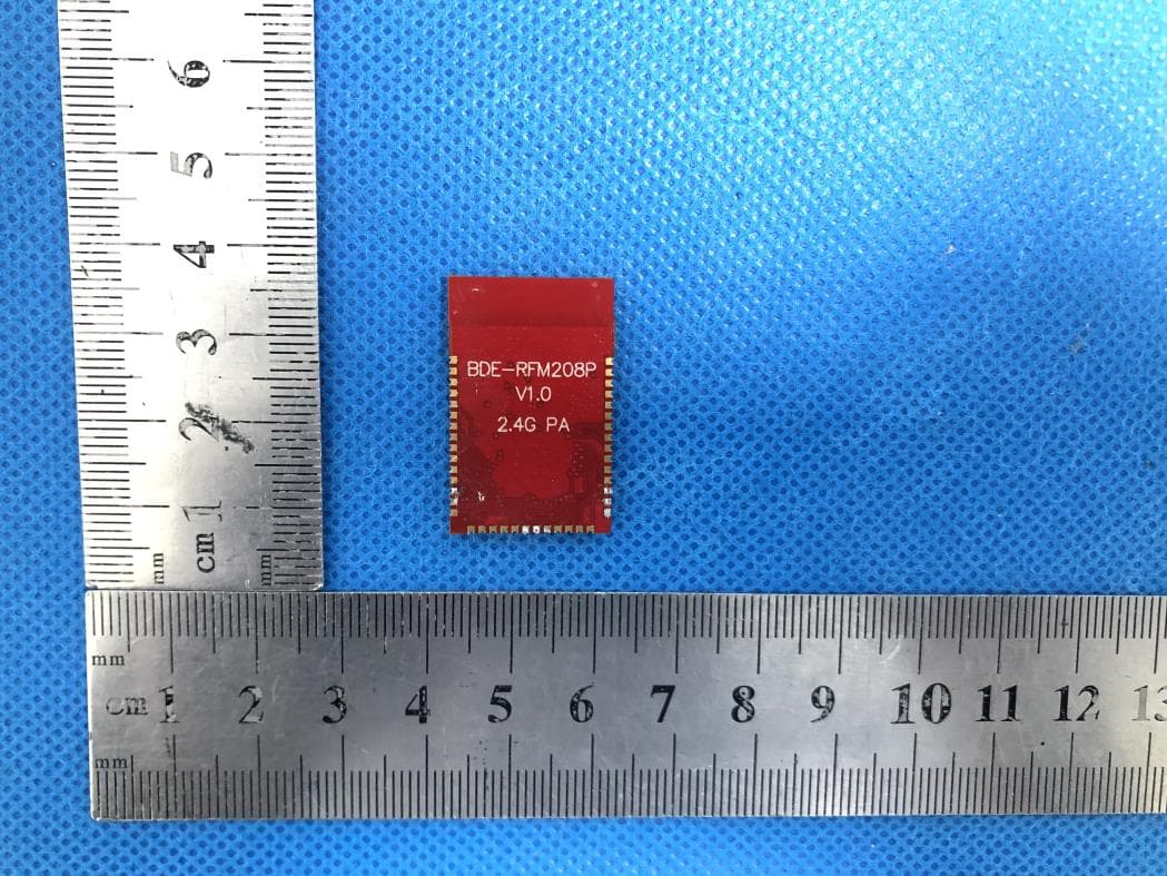
2ABRU-RFM208P24
May 12, 2021Multi-Band Wireless Module with PA
Equipment Class
DTS - Digital Transmission System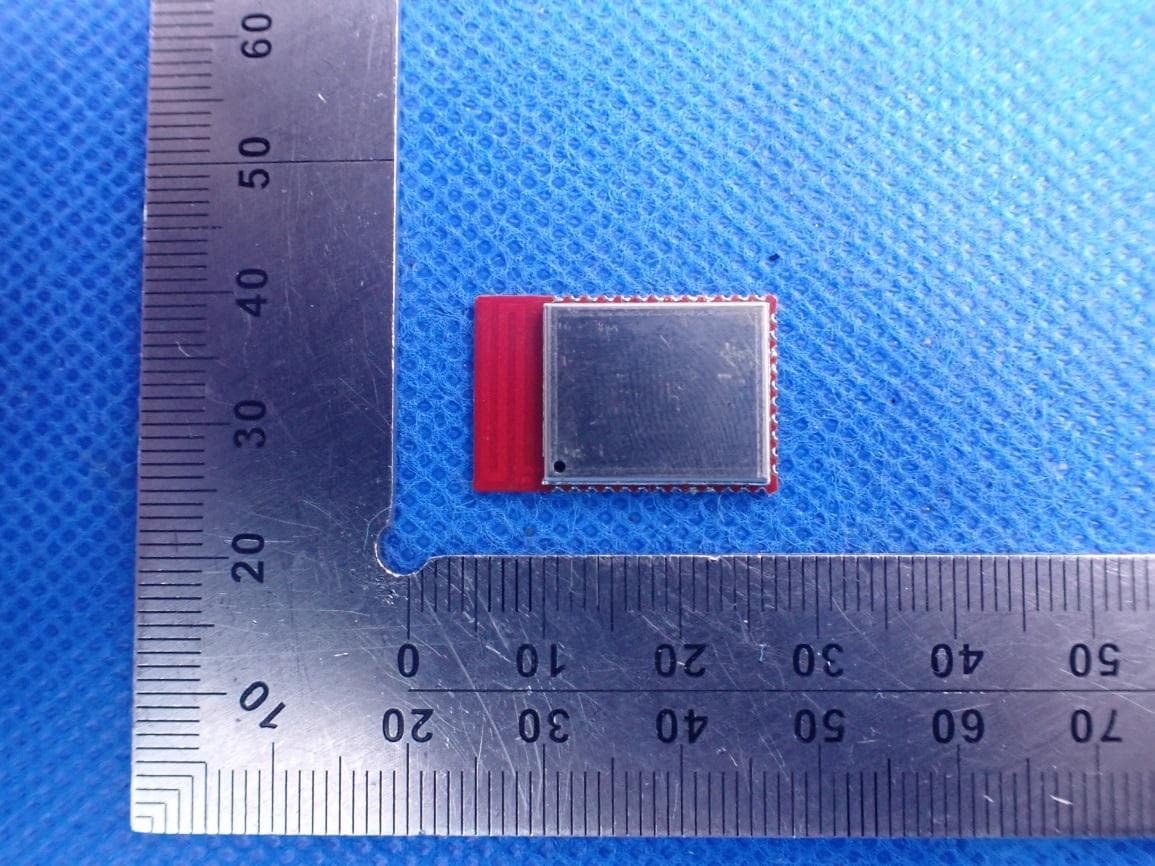
2ABRU-RFM207B
Apr 27, 2021Multiprotocol 2.4G Wireless Module - Industrial Grade
Equipment Class
DTS - Digital Transmission System