2ABY6-RP750XmPOS
Ingenico Inc.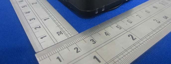
Click to zoom
Application Details
- Equipment Class
- DSS - Part 15 Spread Spectrum Transmitter
- Date of Grant
- Apr 28, 2014
- Application Purpose
- Original Equipment
- Date of Application
- Apr 28, 2014
- Equipment Note
- mPOS
- Frequency Range
- 2402.00000000 - 2480.00000000
- Company
- Ingenico Inc.
- Country
- United States
Documents & Files
Document Text
Text extracted from the exhibit documents filed with the FCC. Open a document above to read the original.
Users Manual
ROAM– 280 Summer St, Boston, MA 02210 Phone: +1.888.589.5885 RP750x USER GUIDE / RP750x• R01 0000 1213 2/17 Copyright © 2013 ROAM Data All rights reserved Contents 1. Introduction __________________________________________________ 3 2. Unpacking ___________________________________________________ 4 3. Recommendations _____________________________________________ 5 3.1. Safety _______________________________________________________________ 5 3.2. Security of your terminal _______________________________________________ 5 3.3. FCC & IC Compliance. __________________________________________________ 6 3.4. Bluetooth SIG ________________________________________________________ 6 3.5. Main Characteristics ___________________________________________________ 8 4. Installation and connection _____________________________________ 9 4.1. Functional description _________________________________________________ 9 9 4.2. Charging Terminal _____________________________________________________ 9 4.3. Terminal in its environment _____________________________________________ 9 4.4. Power on ___________________________________________________________ 10 4.5. Connection _________________________________________________________ 11 4.5.1. USB cable connection ___________________________________________________________ 11 4.5.2. Cable disconnection ____________________________________________________________ 11 5. Daily use ____________________________________________________ 12 5.1. Getting started with RP750x ___________________________________________ 12 5.2. Using Bluetooth on RP750x ____________________________________________ 12 5.3. Terminal keypad _____________________________________________________ 13 5.4. Card reading ________________________________________________________ 14 5.4.1. Swiping a card ________________________________________________________________ 14 5.4.2. Inserting a chip card ___________________________________________________________ 14 6. Maintenance _________________________________________________ 15 6.1. Cleaning of the terminal _______________________________________________ 15 6.2. Transport and storage ________________________________________________ 15 6.3. Troubleshooting _____________________________________________________ 15 6.4. Environment (WEEE, Batteries and Packaging) ____________________________ 16 / RP750x• R01 0000 1213 3/17 Copyright © 2013 ROAM Data All rights reserved 1. Introduction Thank you for choosing a ROAM mobile payment terminal. We recommend that you to read carefully this installation guide: It will give you the necessary information about safety precautions, unpacking, installation and maintenance of your terminal. WARRANTY / SECURITY In order to benefit from the product‐related guaranteeand to respect security, we ask you to use only accessories delivered in box with the product, entrusting maintenance operations only to an authorized person. RP750xis battery powered, use only ROAMparts for replacement: RP750xcan be powered via μUSB. RP750x can be charged with the μUSB cable connected to a mobile phone charger. Failure to comply with these instructions will void the manufacturer’s responsibility. This symbol indicates an important Warning. This symbol indicates a piece of advice. / RP750x• R0 2. Un ADVICE Carefully k shipped. RP750x ran Following An option a with third ADVICE Your termi protective Film prese The RP750x 01 0000 1213 npackin keep the RP nge includes items are in al audio cabl part device inal is delive film to ensu nce does no x terminal ng 750x origina s RP750x, RP cluded in th le might also via audio jac ered with a p ure optimum ot alter in an 4/17 al packaging P750c, RP75 e RP750xb o o be include ck. protective s m protection yway the us μUSB g. It must be 5x, RP755c, ox: ed for termin ee through n of your ter se of the term B cable e re‐used w RP757x, RP7 nals that sup film. We ad minal. minal. T Copyright © 2 Al henever the 757c devices pport comm dvise that yo This User gu 2013 ROAM Data l rights reserved e terminal is s unication ou leave this ide a d s s / RP750x• R01 0000 1213 5/17 Copyright © 2013 ROAM Data All rights reserved 3. Recommendations 3.1. Safety Lithium battery RP750xis fitted with a lithium battery which is not accessible to the user. Only a qualified technician is authorized to open the unit and change this component. Battery RP750x is fitted with a rechargeable Lithium‐ion battery specifically designed for this terminal. It is not accessible to the user. • Only use chargers with rating that match the power ratings. • Do not attempt to open the terminal. • Do not store your terminal unattended in a vehicle. • If the battery has to be replaced, this operation requires to be performed by qualified staff. Warning Risk of explosion if battery is replaced by an incorrect type, do not disassemble, use specified charger only, do not short‐circuit, do not dispose of in fire, do not throw in water, dispose of used batteries according to the instructions. 3.2. Security of your terminal Upon receipt of your terminal you should check for signs of tampering of the equipment. It is strongly advised that these checks are performed regularly. You should check, for example: that the keypad is firmly in place; that there is no evidence of unusual wires that have been connected to any ports on your terminal or associated equipment, the chip card reader, or any other part of your terminal. Such checks would provide warning of any unauthorised modifications to your terminal, and other suspicious behaviour of individuals that have access to your terminal. Your terminal detects any “tampered state”. In this state the terminal will repeatedly flash the message” Alert Interruption!” and further use of the terminal will not be possible. If you observe the “Alert Interruption!” message, you should contact the terminal helpdesk immediately. You are strongly advised to ensure that privileged access to your terminal is only granted to s…
Text truncated - open the document above for the full version.
Block Diagram
CPU 27.12MHz Quartz Resonator 3.3V Power EMC filter Matching circuit Antenna coil Receive circuit IRQ RST CS MOSI MISO CLK XTI XTO RX 13.56M square wave Oscillator 13.56M clock generation transmiter Transmitter control Receive block 13.56M sine wave 13.56M sine wave 13.56M carrier Power block ISSC1677 IIC EEPROM MFI cp GPIO UART Matching 3.3V Power
External Photos
EXHIBIT B - EUT EXTERNAL PHOTOGRAPHS EUT – All View EUT – Top View EUT – Bottom View EUT – Right Side View EUT – Left Side View
ID Label/Location Info
EXHIBIT A - FCC ID LABELING AND LOCATION FCC ID Label Proposed FCC ID Label Location The label shown shall be permanently affixed at a conspicuous location on the device and be readily visible to the user at the time purchase (Labeling requirements per 2.925) Label Here
Internal Photos
EXHIBIT C - EUT INTERNAL PHOTOGRAPHS EUT – Uncover View EUT – Cover Off View EUT – All Board Off View EUT –Main Board Top View EUT –Main Board Bottom View EUT – Sub Board Top View EUT – Sub Board Bottom View EUT – Screen View EUT – Battery View EUT – BT Antenna View EUT – RFID Atenna View
Operational Description
RF part structure picture of model: The iSSC BM77SPP03MC2 Bluetooth module is design for Bluetooth standard SPP/ BLE electronic accessories via Bluetooth connectivity. It is available in the 2.4GHz ISM band Class 2 Radio, compatible with Bluetooth Core Specification Version 3.0/ 4.0 + EDR. iSSC IS1677NM single chip solution combines transceiver and baseband function to decrease the external components. It narrows down the module size and minimizes its cost. The optimized power design minimize power consumption to keep low battery 1. matching circuit The antenna matching circuit is capable of matching with an antenna better and enabling the antenna to receive radio frequency signals better. In fact,The antenna matching circuit is connected between the antenna and the issc1677 model can match the receiving capacity of the antenna to the optimum and effectively reduce the antenna standing wave ratio. 2. IIC circuit The circuit is used to configure the necessary information for the Bluetooth , such as operating mode, sniff interval, SSID, password, etc. parameters so that the module meets the requirements of customers 3. MFI cp MFI chip interface set aside to meet some customers BT3.0 Apple device needs to connect 4. UART GPIO Used to control Bluetooth module and transfer the data communication before between Bluetooth and master MCU b, GPIO module is used to control access to various work,and response the current Bluetooth work status . Matching ISSC1677M 16MHz XTAL IIC EEPROM MFI cp UART GPIO Circuit description Contactless reader part structure picture of model: This radio’s frequency range is 13.56MHzേ7k. 1、The crystal resonator We use a crystal resonator to generate a 27.12MHz clock for the contactless reader part. The contactless chipas3911 divide the clock to a 13.56MHz clock which is used as the carrier signal. 2、The transmitting circuit The transmitting pins of as3911 generate a 13.56MHz square wave. The signal firstly pass the EMC filter which filters the high order harmonic of 13.56MHz, then be sent to the antenna coil by the matching circuit. The antenna transmits out the 13.56MHz carrier signal to the air. 3、The receiving circuit The receiving circuit is a voltage division circuit actually. The contactless card’s response signal is received by the antenna coil. However, the voltage on the antenna is too high for the contactless chip as3911 to receive and decode the card signal. The receiving circuit reduces the voltage to a suitable voltage for receiving. 4、Microprocessor(MPU) The CPU system controls the function of radio using SPI interface.
Schematics
55 44 33 22 11 D D C C B B A A EZP_CS_b default: High E5E6 L10 closed to CPU closed to CPUclosed to CPUclosed to CPU closed to CPUclosed to CPU INNER LDO PRIMALY FLASHSECONDLY FLASHRF K21D:DEPOPK21F:populated DebugBT DEPOP DEPOP DEPOPsecurity domain DEPOPsecurity domain closed to CPU V1.20: 1.03V EXTAL32 Vcoin_ADCEn D-D+VREFH XTAL0EXTAL0 XTAL32 /RST_MAIN ADC_VBAT Vcoin_ADCEn ADC_VBAT VBAT_PIN SPI0_CLK [1,5,6,12,13] SPI0_MISO [1,5] SPI0_MOSI [1,5,6] TCLK/BT_STATUS [12,13] TMS/AUDIO_INT [9,13] TDO/ICC_CS [3,13] EZP_CS_b/ICC_CMD [3,13] ICC_INT [3] ICC_CLK [3] BT_CONFIG [12,13] ICC_IO [3] /ICC_RST [3] ICC_SEL3V_5V [3,10] ICC_SEL1.8V [3,10] SPEAK_ON [12,13] LCD_AD [6] ADC_LiBAT [2] /SPI0_CS2 [12,13] /LCD_CS [6] AUDIO_CAP1 [10] MAG1_DATA1 [4] LCD_LED [6] MAG1_DATA2/MAG3_DATA [4] MAG1_DATA3/MAG3_STROBE [4] CLKOUT [5] AUDIO_CAP2 [10] KB_LINE0 [7] KB_LINE1 [7] KB_ENTER [7] PWR_EN [2] /SPI0_CS0 [5] SPI0_MISO [1,5] SPI0_CLK [1,5,6,12,13] SPI0_MOSI [1,5,6] RF_INT [5] BT_BOOT/RTS [12,13] USB_EN [10] CHARGE_STATUS2 [2,13] CHARGE_STATUS1 [2,13] UART3_TX/USB_ID [12,13] UART3_RX [12,13] /BT_RST [12,13] /CHARGE_ENABLE [2,13] AUDIO_OUT [9] /RESET [1,7,13] TAMPER0 [11] TAMPER1 [11] TAMPER2 [11] USBD- [8,13] USBD+ [8,13] AUDIO_IN [9] TDI/BT_EAN [12,13] /RESET_OUT [1,6,12,13] /RESET_OUT [1,6,12,13] /SPI0_CS1 [1] /SPI0_CS1 [1] BT_STANDBY/CTS [12,13] UART2_TX [12,13] UART2_RX [12,13] BT_SLEEP [12,13] BT_INT [12,13] BT_PWREN [12,13] KB_ROW0 [7] KB_ROW1 [7] KB_ROW2 [7] KB_ROW3 [7] KB_LINE2 [7] KB_LINE3 [7] SPI0_MISO_S [12,13] SPI0_MOSI_S [12,13] /RESET_OUT [1,6,12,13] SAMC_CS [3] VBAT 3.3V 3.3V 3.3V A3.3V 3.3V VOUT33 A3.3V 3.3V VOUT33 3.3V 3.3V A3.3V 3.3V VCC_BAT VBAT C126104C126104 R113 33R113 33 K21P81M50SF4 U1 K21P81M50SF4 U1 PTA0/UART0_CTS_B/UART0_COL_B/FTM0_CH5/JTAG_TCLK/SWD_CLK/EZP_CLK J6 PTA1/UART0_RX/FTM0_CH6/JTAG_TDI/EZP_DI H8 PTA2/UART0_TX/FTM0_CH7/JTAG_TDO/TRACE_SWO/EZP_DO J7 PTA3/UART0_RTS_B/FTM0_CH0/JTAG_TMS/SWD_DIO H9 PTA4/LLWU_P3/FTM0_CH1/NMI_B/EZP_CS_B J8 PTA5/USB_CLKIN/FTM0_CH2/I2S0_TX_BCLK/JTAG_TRST_B K7 PTA12/FTM1_CH0/I2S0_TXD0/FTM1_QD_PHA K8 PTA13/LLWU_P4/FTM1_CH1/I2S0_TX_FS/FTM1_QD_PHB L8 PTA14/SPI0_PCS0/UART0_TX/I2S0_RX_BCLK/I2S0_TXD1 K9 PTA15/SPI0_SCK/UART0_RX/I2S0_RXD0 L9 PTA16/SPI0_SOUT/UART0_CTS_B/UART0_COL_B/I2S0_RX_FS/I2S0_RXD1 J10 PTA17/SPI0_SIN/UART0_RTS_B/I2S0_MCLK H10 EXTAL0/PTA18/FTM0_FLT2/FTM_CLKIN0/ L11 XTAL0/PTA19/FTM1_FLT0/FTM_CLKIN1/LPTMR0_ALT1 K11 ADC0_SE8/PTB0/LLWU_P5/I2C0_SCL/FTM1_CH0/FTM1_QD_PHA G11 ADC0_SE9/PTB1/I2C0_SDA/FTM1_CH1/FTM1_QD_PHB G10 ADC0_SE12/PTB2/I2C0_SCL/UART0_RTS_B/FTM0_FLT3 G9 ADC0_SE13/PTB3/I2C0_SDA/UART0_CTS_B/UART0_COL_B/FTM0_FLT0 G8 PTB10/SPI1_PCS0/UART3_RX/FTM0_FLT1 D10 PTB11/SPI1_SCK/UART3_TX/FTM0_FLT2 C10 PTB12/UART3_RTS_B/FTM1_CH0/FTM0_CH4/FTM1_QD_PHA B11 PTB13/UART3_CTS_B/FTM1_CH1/FTM0_CH5/FTM1_QD_PHB C11 PTB16/SPI1_SOUT/UART0_RX/FTM_CLKIN0/EWM_IN B10 PTB17/SPI1_SIN/UART0_TX/FTM_CLKIN1/EWM_OUT_B E9 PTB18/FTM2_CH0/I2S0_TX_BCLK/FTM2_QD_PHA D9 PTB19/FTM2_CH1/I2S0_TX_FS/FTM2_QD_PHB C9 ADC0_SE14/PTC0/SPI0_PCS4/PDB0_EXTRG/I2S0_TXD1 B9 ADC0_SE15/PTC1/LLWU_P6/SPI0_PCS3/UART1_RTS_B/FTM0_CH0/I2S0_TXD0 D8 ADC0_SE4B/CMP1_IN0/PTC2/SPI0_PCS2/UART1_CTS_B/FTM0_CH1/I2S0_TX_FS C8 CMP1_IN1/PTC3/LLWU_P7/SPI0_PCS1/UART1_RX/FTM0_CH2/CLKOUT/I2S0_TX_BCLK B8 PTC4/LLWU_P8/SPI0_PCS0/UART1_TX/FTM0_CH3/CMP1_OUT A8 PTC5/LLWU_P9/SPI0_SCK/LPTMR0_ALT2/I2S0_RXD0/CMP0_OUT/FTM0_CH2 D7 CMP0_IN0/PTC6/LLWU_P10/SPI0_SOUT/PDB0_EXTRG/I2S0_RX_BCLK/I2S0_MCLK C7 CMP0_IN1/PTC7/SPI0_SIN/USB_SOF_OUT/I2S0_RX_FS B7 CMP0_IN2/PTC8/I2S0_MCLK A7 CMP0_IN3/PTC9/I2S0_RX_BCLK/FTM2_FLT0 D6 PTC10/I2C1_SCL/I2S0_RX_FS C6 PTC11/LLWU_P11/I2C1_SDA/I2S0_RXD1 C5 PTC12 B6 PTC13 A6 PTC16/UART3_RX D5 PTC17/UART3_TX C4 PTD0/LLWU_P12/SPI0_PCS0/UART2_RTS_B D4 ADC0_SE5B/PTD1/SPI0_SCK/UART2_CTS_B D3 PTD2/LLWU_P13/SPI0_SOUT/UART2_RX/I2C0_SCL C3 PTD3/SPI0_SIN/UART2_TX/I2C0_SDA B3 ADC0_SE21/PTD4/LLWU_P14/SPI0_PCS1/UART0_RTS_B/FTM0_CH4/EWM_IN A3 ADC0_SE6B/PTD5/SPI0_PCS2/UART0_CTS_B/UART0_COL_B/FTM0_CH5/EWM_OUT_B A2 ADC0_SE7B/PTD6/LLWU_P15/SPI0_PCS3/UART0_RX/FTM0_CH6/FTM0_FLT0 B2 ADC0_SE22/PTD7/CMT_IRO/UART0_TX/FTM0_CH7/FTM0_FLT1 A1 ADC0_SE10/PTE0/SPI1_PCS1/UART1_TX/TRACE_CLKOUT/I2C1_SDA/RTC_CLKOUT E4 ADC0_SE11/PTE1/LLWU_P0/SPI1_SOUT/UART1_RX/TRACE_D3/I2C1_SCL/SPI1_SIN E3 ADC0_DP1/PTE2/LLWU_P1/SPI1_SCK/UART1_CTS_B/TRACE_D2 E2 ADC0_DM1/PTE3/SPI1_SIN/UART1_RTS_B/TRACE_D1/SPI1_SOUT F4 PTE4/LLWU_P2/SPI1_PCS0/UART3_TX/TRACE_D0 H7 PTE5/SPI1_PCS2/UART3_RX G4 ADC0_SE4A/PTE16/SPI0_PCS0/UART2_TX/FTM_CLKIN0/FTM0_FLT3 K3 ADC0_SE5A/PTE17/SPI0_SCK/UART2_RX/FTM_CLKIN1/LPTMR0_ALT3 H4 ADC0_SE6A/PTE18/SPI0_SOUT/UART2_CTS_B/I2C0_SDA A11 ADC0_SE7A/PTE19/SPI0_SIN/UART2_RTS_B/I2C0_SCL A10 ADC0_DM0 K2 ADC0_DM3 L2 ADC0_DP0 K1 ADC0_DP3 L1 DAC0_OUT/CMP1_IN3/ADC0_SE23 K5 EXTAL32 L5 RESET J11 TAMPER0/RTC_WAKEUP_B L7 TAMPER1 H5 TAMPER2 J5 USB0_DM F2 USB0_DP F1 VBAT K6 VOUT33 G1 VREF_OUT/CMP1_IN5/CMP0_IN5 L3 VREFH G5 VREFL G6 VREGIN G2 XTAL32 L4 VSS_1 G3 VSS_2 G7 VSS_3 K10 VSS_4 L6 VSSA F6 VDD_1 E5 VDD_2 E6 VDD_3 L10 VDDA F5 NC_1 A4 NC_2 A5 NC_3 A9 NC_4 B1 NC_5 B4 NC_6 B5 NC_7 C1 NC_8 C2 NC_9 D1 NC_10 D2 NC_11 D11 NC_12 E1 NC_13 E7 NC_14 E8 NC_15 E10 NC_16 E11 NC_17 F3 NC_18 F7 NC_19 F8 NC_20 F9 NC_21 F10 NC_22 F11 NC_23 H1 NC_24 H2 NC_25 H3 NC_26 H6 NC_27 H11 NC_28 J1 NC_29 J2 NC_30 J3 NC_31 J4 NC_32 J9 NC_33 K4 C13 22pF C13 22pF C8104C8104 Q35PMBT3906Q35PMBT3906 1 23 Y1 32.768K Y1 32.768K 23 14 R316 4.7K F R316 4.7K F R5 33 R5 33 C310uF/10VC310uF/10V C4104C4104 C15104C15104 C11104C11104 R318100K FR318100K F C9104C9104 R3141MR3141M C13210uF/10VC13210uF/10V C115270pF/50VC115270pF/50V FB1 600ohm/500mA FB1 600ohm/500mA C1105C1105 R3 33 R3 33 R1416.8K FR1416.8K F R315 470KR315 470K Y2 27.12MHZ Y2 27.12MHZ 23 14 R321 100R321 100 R2 33 R2 33 W25Q64FV U2 W25Q64FV U2 /CS 1 DO(IO1) 2 /WP(IO2) 3 GND 4 DI(IO0) 5 CLK 6 /HOLD(IO3) 7 VCC 8 10K10K Q36 PDTC114ET 10K10K Q36 PDTC114ET 1 23 R14215K FR14215K F R7 33 R7 33 C2104C2104 C14 22pF C14 22pF R320 100 R320 100 C12 10uF/10V C12 10uF/10V R6 33 R6 33 C113104C113104 R4 33 R4 33 R111 33R111 33 R1 33 R1 33 R154 33R154 3…
Text truncated - open the document above for the full version.
Test Report
Note: This test report is prepared for the customer shown above and for the device described herein. It may not be duplicated or used in part without prior written consent from Bay Area Compliance Laboratories Corp. This report must not be used by the customer to claim product certification, approval, or endorsement by NVLAP*, or any agency of the Federal Government. * This report may contain data that are not covered by the NVLAP accreditation and shall be marked with an asterisk “★” (Rev.2). This report is valid only with a valid digital signature. The digital signature may be available only under the Adobe software above version 7.0. FCC PART 15.247 TEST REPORT For Roam Data Inc. 280 Summer St Boston, Massachusetts FCC ID: 2ABY6-RP750X Report Type: Original Report Product Type: mPOS Test Engineer: Leon Chen Re port Number: R2XM140224050-00B Re port Date: 2014-03-21 Reviewed By: Ivan Cao RF Leader Test Laboratory: Bay Area Compliance Laboratories Corp. (Dongguan) No.69 Pulongcun, Puxinhu Industrial Zone, Tangxia, Dongguan, Guangdong, China Tel: +86-769-86858888 Fax: +86-769-86858891 www.baclcorp.com.cn Bay Area Compliance Laboratories Corp. (Dongguan) Report No.: R2XM140224050-00B FCC Part 15.247 Page 2 of 54 TABLE OF CONTENTS GENERAL INFORMATION ....................................................................................................................................... 4 PRODUCT DESCRIPTION FOR EQUIPMENT UNDER TEST (EUT) ..................................................................................... 4 OBJECTIVE ................................................................................................................................................................... 4 RELATED SUBMITTAL(S)/GRANT(S) ............................................................................................................................. 4 TEST METHODOLOGY .................................................................................................................................................. 4 TEST FACILITY ............................................................................................................................................................. 5 SYSTEM TEST CONFIGURATION .......................................................................................................................... 6 DESCRIPTION OF TEST CONFIGURATION ...................................................................................................................... 6 EUT EXERCISE SOFTWARE .......................................................................................................................................... 6 EQUIPMENT MODIFICATIONS ....................................................................................................................................... 6 SUPPORT EQUIPMENT LIST AND DETAILS .................................................................................................................... 6 EXTERNAL CABLE ........................................................................................................................................................ 6 BLOCK DIAGRAM OF TEST SETUP ................................................................................................................................ 7 SUMMARY OF TEST RESULTS ............................................................................................................................... 8 FCC §15.247 (i) & §1.1310 & §2.1093- RF EXPOSURE ............................................................................................... 9 APPLICABLE STANDARD .............................................................................................................................................. 9 FCC §15.203 - ANTENNA REQUIREMENT ........................................................................................................... 10 APPLICABLE STANDARD ............................................................................................................................................ 10 ANTENNA CONNECTOR CONSTRUCTION .................................................................................................................... 10 FCC §15.207 (a) – AC LINE CONDUCTED EMISSIONS ..................................................................................... 11 APPLICABLE STANDARD ............................................................................................................................................ 11 MEASUREMENT UNCERTAINTY .................................................................................................................................. 11 EUT SETUP ................................................................................................................................................................ 11 EMI TEST RECEIVER SETUP ....................................................................................................................................... 12 TEST PROCEDURE ...................................................................................................................................................... 12 CORRECTED AMPLITUDE & MARGIN CALCULATION ................................................................................................. 12 TEST EQUIPMENT LIST AND DETAILS ......................................................................................................................... 13 TEST RESULTS SUMMARY .......................................................................................................................................... 13 TEST DATA ................................................................................................................................................................ 13 FCC §15.209, §15.205 & §15.247(d) - SPURIOUS EMISSIONS ............................................................................. 16 APPLI…
Text truncated - open the document above for the full version.
Test Setup Photos
EXHIBIT D - TEST SETUP PHOTOGRAPHS Conducted Emissions - Front View Conducted Emissions – Side View Radiated Emission -Front View (Below 1GHz) Radiated Emission - Rear View (Below 1GHz) Radiated Emission -Front View (Above 1GHz) Radiated Emission - Rear View (Above 1GHz)
Contact Information
Applicant
Christopher ROTSAERT(VP of HW Product Management & Supply chain)
Test Firm
Bay Area Compliance Laboratories Corp. (Dongguan)John Chan
[email protected]86-769-86858888
Technical Specifications
| # | Rule Parts | Frequency Range | Power Output |
|---|---|---|---|
| 1 | 15C | 2.40 GHz - 2.48 GHz | 1.00 mW |
Other Applications from Ingenico Inc.
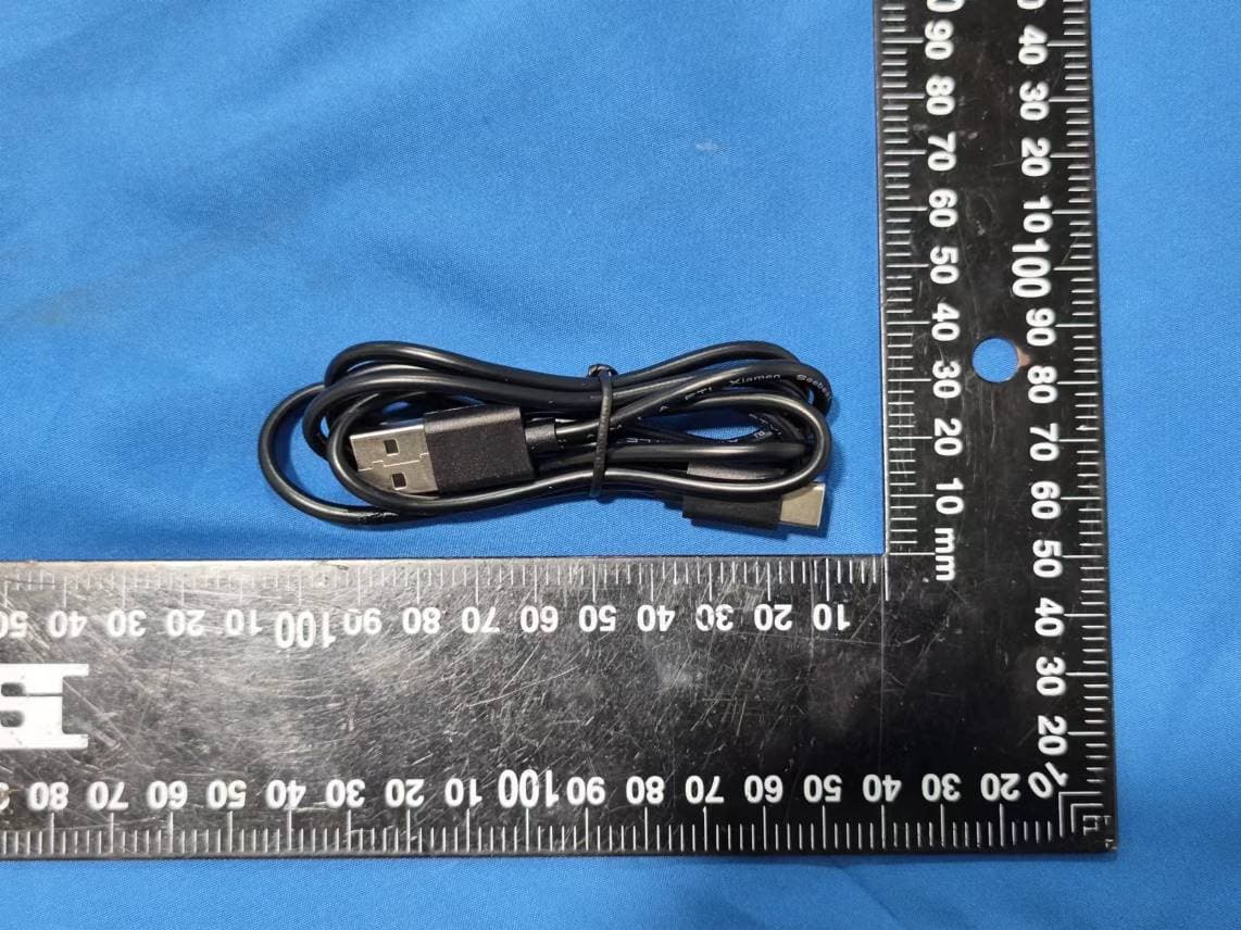
2ABY6-MOB55CL3
Jul 13, 2023Mobile Payment Terminal
Equipment Class
DSS - Part 15 Spread Spectrum Transmitter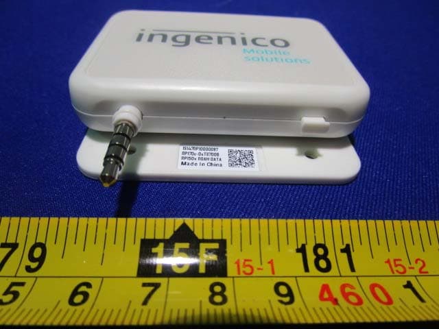
2ABY6-RP170C
Aug 24, 2015Mobile Payment Terminal
Equipment Class
DXX - Part 15 Low Power Communication Device Transmitter