2AD56HLK-M30WIFI module
Shenzhen Hi-Link Electronic co., Ltd.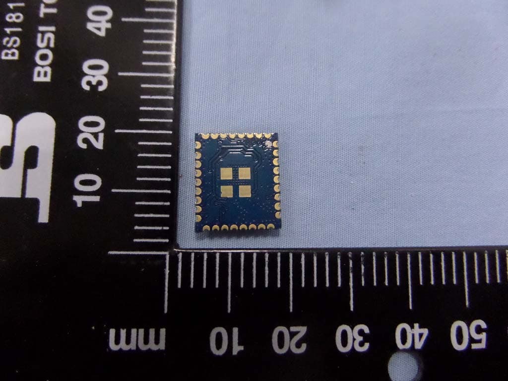
Click to zoom
Application Details
- Equipment Class
- DTS - Digital Transmission System
- Date of Grant
- Feb 02, 2015
- Application Purpose
- Original Equipment
- Date of Application
- Feb 02, 2015
- Equipment Note
- WIFI module
- Frequency Range
- 2412.00000000 - 2472.00000000
- Country
- China
Documents & Files
Document Text
Text extracted from the exhibit documents filed with the FCC. Open a document above to read the original.
Users Manual
HLK-M30 Data Sheet HLK-M30-DS V1.0 7/30/2014 Overview: HLK-M30 is a new low-cost embedded UART-WIFI module (serial port -Wireless) developed by Shenzhen HaiLingKe Electronic co., Ltd. This product is an embedded module based on the universal serial interface network standard,built-in TCP / IP protocol stack, enabling the user serial port,wireless network (wifi) interface between the onversions.Through the HLK-M30 module, the traditional serial devices do not need to change any configuration,userdata can be transmitted through the Internet network. Provide a quick solution for the user’s serial devices to transfer data via WIFI Module Block Diagram Applications • WiFi Led Control • WiFi Power Switch • Smart Home;Smart Buliding • OBDII WiFi Diagnose • RFID Data Transfer • Toys and Gaming Peripherals • Industrial Systems • Telemetry • Remote Control Benefits • Low Power consumption • Ready to use in products • Minimizes product development • No RF test required for systems • Serial to Wifi; Smart;Small; • Support Smart Connection • Transparent Transmission • Serial to Wifi; Smart;Small; • Compliant with CE and FCC Features: • 2.4GHz 802.11b/g/n,compatible • WiFi Sta/Soft AP Mode • Support Smart Connection • The range of baudrate: 1200~115200bps • Support transparent transmission mode • Support multiple security authenti-cation mechanisms: WEP64/WEP128/ TKIP/ AES WEP/WPA-PSK/WPA2-PSK • Support wireless roam • Support multiple network protocols: TCP/UDP/ /DHCP/DNS • Support AT instruction Set • Device Dimensions 16.3mm*14mm* 2.24mm Lead-free and RoHS compliant HLK-M30 Data Sheet HLK-M30-DS V1.0 7/30/2014 1. Introduction The HLK-M30 module provides designers with a ready made component that provides a fully integrated solution for applications, using the IEEE802.11 standard in the 2.4-2.5GHz ISM frequency band, including802.11b/g/n, can be quickly and easily included in product designs. The modules integrate all of the RF components required, removing the need to perform expensive RF design and test. Products can be designed by simply connecting sensors and switches to the module IO pins or uart interface. The modules use MTK’s chip Wireless Microcontroller, allowing designers to make use of the serial interface to connect with their device. Hence, this module allows designers to bring wireless applications to market in the minimum time with significantly reduced development effort and cost. The HLK-M30 is an embedded module based on the universal serial interface network standard,built-in TCP / IP protocol stack, enabling the user serial port, wireless network (wifi) interface between the conversions. Through the HLK-M30 module, the traditional serial devices do not need to change any configuration; data can be transmitted through the Internet network. Provide a quick solution for the user’s serial devices to transfer data via Ethernet Also the HLK-M30 module have FCC modular approvals and is compliant with EU regulations. 2. Specifications The parameters are defined here. VDD=3.3V @ +25°C Typical DC Characteristics Notes RX Active, HT40, MCS7 150mA 802.11.n TX HT40, MCS7 @15dBm 210mA 802.11.n Typical RF Characteristics Notes Receive sensitivity -70dBm(802.11n) Use IQview to adjust Maximum Transmit power 18dBm/15dBm/13.5dBm 802.11b/g/n RF Port impedance – Ipex onnector 50 ohm 2.4 - 2.5GHz VSWR (max) 2:1 2.4 - 2.5GHz Centre frequency accuracy +/-25ppm Additional +/-15ppm allowance Peripherals Notes UART 2pins 1200-115200kbps GPIO 5pins GPIO VCC 2pins 3.3V+/-10% Two VCC should all connect to power AN 4pins Analog GND 23pins GND HLK-M30 Data Sheet HLK-M30-DS V1.0 7/30/2014 3. Product Development HaiLingKe supplies all the development tools needed to enable end-product development to occur quickly and efficiently. These are all available from www.hlktech.com. A evaluation kits is also available, allowing products to be quickly bread boarded. Efficient development of software applications is enabled by the provision of a complete, unlimited, software developer kit.This package provides everything required to develop application code and to trial it with hardware representative of the final module. 4. Pin Layout Note:VDD1 and VDD2 should all connect to 3.3V. Pin 35/36/37/38 is GND. 4.1. Pin Description Pin No Signal Type Description 1 GPIO1 General GPIO 2 GPIO0 General GPIO GPIO1 GPIO0 GND GND GND GND GND GND GND GND GND GND GND VDD1 AN4 GND VDD2 1 2 3 4 5 6 7 8 9 10 11 12 13 14 15 16 17 18 19 20 21 22 23 24 25 26 27 28 29 30 31 32 33 34 35 37 36 38 GND GND GND GND AN1 AN2 AN3 GPIO2 ES/RST LED TX RX RST GND GND GND ANT HLK-M30 Data Sheet HLK-M30-DS V1.0 7/30/2014 3 GND Analogue Ground 4 GND Analogue Ground 5 GND Analogue Ground 6 GND Analogue Ground 7 VDD2 Supply Voltage, 3.3V+/-10% 8 GND Analogue Ground 9 ANT Antenna Pin 10 GND Analogue Ground 11 GND Analogue Ground 12 GND Analogue Ground 13 GND Analogue Ground 14 GND Analogue Ground 15 AN1 Analogue Pin(Reserved) 16 AN2 Analogue Pin(Reserved) 17 AN3 Analogue Pin(Reserved) 18 AN4 Analogue Pin(Reserved) 19 VDD1 Supply Voltage, 3.3V+/-10% 20 GND Analogue Ground 21 GND Analogue Ground 22 GND Analogue Ground 23 GND Analogue Ground 24 GND Analogue Ground 25 GND Analogue Ground 26 GND Analogue Ground 27 GND Analogue Ground 28 GND Analogue Ground 29 RST_N Reset Module 30 RX UART RX 31 TX UART TX 32 LED Staus LED 33 ES/RST Exit/Default/Update 34 GPIO2 General GPIO 35 GND Analogue Ground 36 GND Analogue Ground 37 GND Analogue Ground 38 GND Analogue Ground FCC Warning This device complies with Part 15 of the FCC Rules. Operation is subject to the following two conditions: (1) this device may not cause harmful interference, and (2) this device must accept any interference received, including interference that may cause undesired operation. NOTE: Any changes or modifications to this unit not expressly approved by the party responsible for compliance could void the user's authority to operate the equipment. FCC Radiation Exposure Statement: This equipment compl…
Text truncated - open the document above for the full version.
External Photos
Shenzhen Hi-Link Electronic co., Ltd Model: HLK-M30 REPORT NO.: STR14128107I FCC PART 15.247 EXHIBIT 2 - EUT EXTERNAL PHOTOGRAPHS EUT View 1 EUT View 2 Shenzhen Hi-Link Electronic co., Ltd Model: HLK-M30 REPORT NO.: STR14128107I FCC PART 15.247 EUT View 3
ID Label/Location Info
Shenzhen Hi-Link Electronic co., Ltd Model: HLK-M30 REPORT NO.: STR14128107I FCC PART 15.247 EXHIBIT 1 - PRODUCT LABELING Proposed FCC ID Label Format FCC ID: 2AD56HLK-M30 Specifications: Text is Black in color and justified. Labels are printed in indelible ink on permanent adhesive silk-screened onto the EUT or shall be affixed at a conspicuous location on the EUT. Proposed Label Location on EUT FCC ID Label Location
ID Label/Location Info
Shenzhen Hi-Link Electronic co., Ltd Model: HLK-M30 REPORT NO.: STR14128107I FCC PART 15.247 EXHIBIT 1 - PRODUCT LABELING Proposed FCC ID Label Format FCC ID: 2AD56HLK-M30 Specifications: Text is Black in color and justified. Labels are printed in indelible ink on permanent adhesive silk-screened onto the EUT or shall be affixed at a conspicuous location on the EUT. Proposed Label Location on EUT FCC ID Label Location
Internal Photos
Shenzhen Hi-Link Electronic co., Ltd Model: HLK-M30 REPORT NO.: STR14128107I FCC PART 15.247 EXHIBIT 3 - EUT INTERNAL PHOTOGRAPHS EUT Housing and Board View 1 Solder Board-Component View 1 Shenzhen Hi-Link Electronic co., Ltd Model: HLK-M30 REPORT NO.: STR14128107I FCC PART 15.247 Solder Board-Component View 2
RF Exposure Info
1. MAXIMUM PERMISSIBLE EXPOSURE (MPE) 1.1 Standard Applicable According to §1.1307(b)(1), system operating under the provisions of this section shall be operating in a manner that the public is not exposed to radio frequency energy level in excess limit for maximum permissible exposure. (a) Limits for Occupational / Controlled Exposure Frequency range (MHz) Electric Field Strength (E) (V/m) Magnetic Field Strength (H) (A/m) Power Density (S) (mW/cm 2 ) Averaging Times | E | 2 , | H | 2 or S (minutes) 0.3-3.0 614 1.63 (100)* 6 3.0-30 1842/f 4.89/f (900/f)* 6 30-300 61.4 0.163 1.0 6 300-1500 / / F/300 6 1500-100000 / / 5 6 (b) Limits for General Population / Uncontrolled Exposure Frequency range (MHz) Electric Field Strength (E) (V/m) Magnetic Field Strength (H) (A/m) Power Density (S) (mW/cm 2 ) Averaging Times | E | 2 , | H | 2 or S (minutes) 0.3-1.34 614 1.63 (100)* 30 1.34-30 824/f 2.19/f (180/f)* 30 30-300 27.5 0.073 0.2 30 300-1500 / / F/1500 30 1500-100000 / / 1 30 Note: f = frequency in MHz: * = Plane-wave equivalents power density 1.2 MPE Calculation Method S = (30*P*G) / (377*R 2 ) S = power density (in appropriate units, e.g., mw/cm 2 ) P = power input to the antenna (in appropriate units, e.g., mw) G = power gain of the antenna in the direction of interest relative to an isotropic radiator, the power gain factor is normally numeric gain. R = distance to the center of radiation of the antenna (in appropriate units, e.g., cm) 1.3 MPE Calculation Result Since the maximum eirp power is used as the output power to antenna, so the Gain of the antenna can be assumed as 0dBi. Maximum peak output power: 14.81 (dBm) Maximum peak output power at antenna input terminal: 30.2691(mW) Prediction distance: >20 (cm) Prediction frequency: 2412 (MHz) Antenna gain (typical): 0 (dBi) Antenna gain (typical): 1 (numeric) The worst case is power density at prediction frequency at 5cm: 0.00602(mw/cm 2 ) MPE limit for general population exposure at prediction frequency: 1 (mw/cm 2 ) 0.00602 (mw/cm 2 ) < 1 (mw/cm 2 ) Result: Pass
Test Report
Shenzhen HaiLingKe Electronic co., Ltd Model: HLK-M30 REPORT NO.: STR14128107I PAGE 1 OF 77 FCC PART 15.247 FCC Part 15C Measurement and Test Report For Shenzhen HaiLingKe Electronic co., Ltd 3F, 5# Buliding, Minxing Industrial Park, MinKang Rd .Minzhi, Longhua District, Shenzhen, China FCC ID: 2AD56HLK-M30 FCC Rule(s): FCC Part 15C Product Description: WIFI module Tested Model: HLK-M30 Report No.: STR14128107I Tested Date: 2014-12-12 to 2014-12-20 Issued Date: 2014-12-20 Tested By: Jong Wang / Engineer Reviewed By: Lahm Peng / EMC Manager Approved & Authorized By: Jandy so / PSQ Manager Prepared By: Shenzhen SEM.Test Technology Co., Ltd. 1/F, Building A, Hongwei Industrial Park, Liuxian 2nd Road, Bao'an District, Shenzhen, P.R.C.(518101) Tel.: +86-755-33663308 Fax.: +86-755-33663309 Website: www.semtest.com.cn Note: This test report is limited to the above client company and the product model only. It may not be duplicated without prior permitted by Shenzhen SEM.Test Technology Co., Ltd. Shenzhen HaiLingKe Electronic co., Ltd Model: HLK-M30 REPORT NO.: STR14128107I PAGE 2 OF 77 FCC PART 15.247 TABLE OF CONTENTS 1. GENERAL INFORMATION ................................................................................................................................... 3 1.1 PRODUCT DESCRIPTION FOR EQUIPMENT UNDER TEST (EUT) ............................................................................... 3 1.2 TEST STANDARDS ................................................................................................................................................... 4 1.3 TEST METHODOLOGY ............................................................................................................................................. 4 1.4 TEST FACILITY ....................................................................................................................................................... 4 1.5 EUT SETUP AND TEST MODE ................................................................................................................................. 5 2. SUMMARY OF TEST RESULTS ........................................................................................................................... 6 3. RF EXPOSURE ......................................................................................................................................................... 7 3.1 STANDARD APPLICABLE ......................................................................................................................................... 7 3.2 TEST RESULT.......................................................................................................................................................... 7 4. ANTENNA REQUIREMENT .................................................................................................................................. 8 4.1 STANDARD APPLICABLE ......................................................................................................................................... 8 4.2 EVALUATION INFORMATION .................................................................................................................................. 8 5. POWER SPECTRAL DENSITY ............................................................................................................................. 9 5.1 STANDARD APPLICABLE ......................................................................................................................................... 9 5.2 TEST EQUIPMENT LIST AND DETAILS ..................................................................................................................... 9 5.3 TEST PROCEDURE ................................................................................................................................................... 9 5.4 ENVIRONMENTAL CONDITIONS .............................................................................................................................. 9 5.5 SUMMARY OF TEST RESULTS/PLOTS .................................................................................................................... 10 6. 6DB BANDWIDTH ................................................................................................................................................. 17 6.1 STANDARD APPLICABLE ....................................................................................................................................... 17 6.2 TEST EQUIPMENT LIST AND DETAILS ................................................................................................................... 17 6.3 TEST PROCEDURE ................................................................................................................................................. 17 6.4 ENVIRONMENTAL CONDITIONS ............................................................................................................................ 17 6.5 SUMMARY OF TEST RESULTS/PLOTS .................................................................................................................... 18 7. RF OUTPUT POWER ............................................................................................................................................ 25 7.1 STANDARD APPLICABLE ....................................................................................................................................... 25 7.2 TEST EQUIPMENT LIST AND DETAILS ................................................................................................................... 25 7.3 TEST PROCEDURE ................................................................................................................................................. 25 7.4 ENVIRONMENTAL CONDITIONS ............................................................................................................................ 25 7.5 SUMMARY OF TEST RESULTS/PLOTS ............…
Text truncated - open the document above for the full version.
Test Setup Photos
Shenzhen Hi-Link Electronic co., Ltd Model: HLK-M30 REPORT NO.: STR14128107I FCC PART 15.247 EXHIBIT 4 - TEST SETUP PHOTOGRAPHS Conducted Emission Test Setup Radiation Emission Test Setup (Below 30MHz) Shenzhen Hi-Link Electronic co., Ltd Model: HLK-M30 REPORT NO.: STR14128107I FCC PART 15.247 Radiation Emission Test Setup (30MHz to 1GHz) Radiation Emission Test Setup (Above 1GHz)
Contact Information
Applicant
Jacky Gong(Manager)
Test Firm
Shenzhen SEM.Test Technology Co., Ltd.Jandy So
Technical Specifications
| # | Rule Parts | Frequency Range | Power Output |
|---|---|---|---|
| 1 | 15C | 2.41 GHz - 2.47 GHz | 21.40 mW |
Other Applications from Shenzhen Hi-Link Electronic co., Ltd.
2AD56-HLK-B40
Jul 01, 2026Bluetooth Module
Equipment Class
DTS - Digital Transmission System
2AD56HLK-B50
Sep 24, 2023Bluetooth module
Equipment Class
DTS - Digital Transmission System
2AD56HLK-L06-915
Jul 12, 2023LoRa Module
Equipment Class
DTS - Digital Transmission System
2AD56HLK-LD2410B-P
Jun 26, 2023Radar Module
Equipment Class
DXX - Part 15 Low Power Communication Device Transmitter
2AD56HLK-LD2410-P
Jun 26, 2023Radar Module
Equipment Class
DXX - Part 15 Low Power Communication Device Transmitter