2ADEKSLEEVES10S10 R(H)
Social Bicycles LLC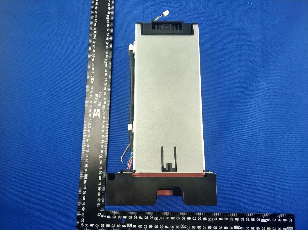
Click to zoom
Application Details
- Equipment Class
- DXX - Part 15 Low Power Communication Device Transmitter
- Date of Grant
- Mar 23, 2020
- Application Purpose
- Original Equipment
- Date of Application
- Mar 23, 2020
- Equipment Note
- S10 R(H)
- Frequency Range
- 13.56000000 - 13.56000000
- Company
- Social Bicycles LLC
- Country
- United States
Documents & Files
Document Text
Text extracted from the exhibit documents filed with the FCC. Open a document above to read the original.
Users Manual
S10 Sleeve Technical Description SK - 9/18/2019 Introduction This document is meant to describe the inner working of the S10 sleeve module. Purpose The JUMP battery pack can be inserted into the S10 sleeve, which will act as the housing mechanism to charge the battery. The purpose of the LED on the front of the S10 sleeve is to indicate the charge SoC status of the JUMP pack. The purpose of the hall effect switch which is activated by a magnet built into the latch assembly, is to gracefully stop charging and turn off the battery before it is removed from the sleeve. The purpose of the two connectors are 1) accepts the output of the charger power 2) other connector transfers signals + power to the rear holster PCBA. Hardware The S10 Sleeve contains two PCBA’s. The first PCB assembly (LED board) is located at the front of the sleeve and primarily contains an LED, power and signal connectors, and hall effect sensor – used as a switch. The second PCB assembly (Holster board) is located at the back of S10 and is the wireless NFC link between the batteries internal BMS and the logic on the holster board. LED communicated via CLK, DATA, 5V and GND which comes from the holster board. The switch sends a logic low transition when the latch is pressed. Hall sensor sends out a logic low signal when latch is depressed (magnet over the hall sensor). Switch GPIO pin is pulled up to 3V3 inside the holster board. Two pin barrel jack, 2.1mm (ID) x 5.5mm (OD) is the 41V5 input of the charger at 3.6A max. The wire harness from the front LED board to the back holster board consist of 7 wires. 41V5, RTN, 5V, GND, CLK, DATA, SWITCH_GPIO Pictures FCC Statement 15.19 1. This device complies with Part 15 of the FCC Rules. Operation is subject to the following two conditions: (1) This device may not cause harmful interference. (2) This device must accept any interference received, including interference that may cause undesired operation. 15.21 Note: The grantee is not responsible for any changes or modifications not expressly approved by the party responsible for compliance. Such modifications could void the user’s authority to operate the equipment. 15.105(b) NOTE: This equipment has been tested and found to comply with the limits for a Class B digital device, pursuant to part 15 of the FCC Rules. These limits are designed to provide reasonable protection against harmful interference in a residential installation. This equipment generates uses and can radiate radio frequency energy and, if not installed and used in accordance with the instructions, may cause harmful interference to radio communications. However, there is no guarantee that interference will not occur in a particular installation. If this equipment does cause harmful interference to radio or television reception, which can be determined by turning the equipment off and on, the user is encouraged to try to correct the interference by one or more of the following measures: - Reorient or relocate the receiving antenna. - Increase the separation between the equipment and receiver. -Connect the equipment into an outlet on a circuit different from that to which the receiver is connected. -Consult the dealer or an experienced radio/TV technician for help
External Photos
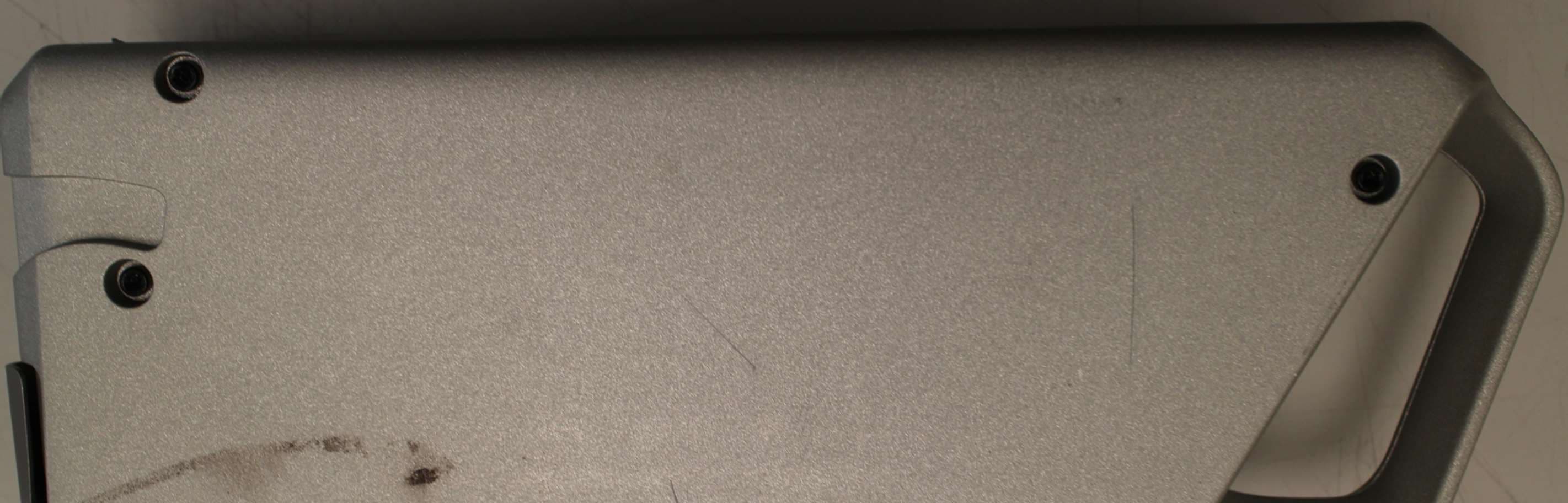
Annex No.: BL-SZ2020242-AW 1 / 3 EUT EXTERNAL PHOTOS FRONT VIEW OF EUT REAR VIEW OF EUT Annex No.: BL-SZ2020242-AW 2 / 3 LEFT SIDE VIEW OF EUT RIGHT SIDE OF EUT Annex No.: BL-SZ2020242-AW 3 / 3 TOP VIEW OF EUT BOTTOM VIEW OF EUT
ID Label/Location Info
Label: Label location:
Internal Photos
Annex No.: BL-SZ2020242-AI 1 / 4 EUT INTERNAL PHOTOS EUT UNCOVER VIEW EUT UNCOVER VIEW Annex No.: BL-SZ2020242-AI 2 / 4 EUT UNCOVER VIEW EUT UNCOVER VIEW Annex No.: BL-SZ2020242-AI 3 / 4 MAIN BOARD TOP VIEW MAIN BOARD REAR VIEW Annex No.: BL-SZ2020242-AI 4 / 4 MAIN BOARD TOP VIEW MAIN BOARD REAR VIEW NFC Antenna RF Chip
RF Exposure Info
RF EXPOSURE EVALUATION 1. PRODUCT INFORMATION Product Description Bicycle charging stand Model Name 2004668 [S10R(H)] FCC ID 2ADEKSLEEVES10 2. EVALUATION METHOD According to 447498 D01 General RF Exposure Guidance v05 the 1-g and 10-g SAR test exclusion thresholds for 100 MHz to 6 GHz at test separation distances ≤ 50 mm are determined by: [(max. power of channel, including tune-up tolerance, mW)/(min. test separation distance, mm)] ·[√f(GHz)] ≤ 3.0 for 1-g SAR and ≤ 7.5 for 10-g extremity SAR. Where f(GHz) is the RF channel transmit frequency in GHz Power and distance are rounded to the nearest mW and mm before calculation 3. CALCULATION Pt= dBm = < 0.1 mW The value of the Maximum output power Pt is referred to the test report of the CFR47 §15.249 No: BL-SZ2020242-402 The result for the evaluation SAR = (<0.1 mW / 5 mm) .[√0.01356 (GHz)] = <0.1 < 3.0 for 1-g SAR and ≤ 7.5 for 10-g extremity SAR. 4. CONCLUSION The SAR evaluation is not required.
Test Report
Report No.: BL-SZ2020242-402 2 / 27 Revision History Version Issue Date Revisions Content Rev. 01 Mar. 23, 2020 Initial Issue TABLE OF CONTENTS 1 ADMINISTRATIVE DATA (GENERAL INFORMATION) .......................................................................... 4 1.1 Identification of the Testing Laboratory .............................................................................................. 4 1.2 Identification of the Responsible Testing Location ............................................................................. 4 1.3 Laboratory Condition .......................................................................................................................... 4 1.4 Announce ........................................................................................................................................... 4 2 PRODUCT INFORMATION ...................................................................................................................... 5 2.1 Applicant Information ......................................................................................................................... 5 2.2 Manufacturer Information ................................................................................................................... 5 2.3 Factory Information ............................................................................................................................ 5 2.4 General Description for Equipment under Test (EUT) ....................................................................... 5 2.5 Technical Information ......................................................................................................................... 6 3 SUMMARY OF TEST RESULTS .............................................................................................................. 7 3.1 Test Standards ................................................................................................................................... 7 3.2 Verdict ................................................................................................................................................ 7 3.3 Test Uncertainty ................................................................................................................................. 7 4 GENERAL TEST CONFIGURATIONS ..................................................................................................... 8 4.1 Test Environments ............................................................................................................................. 8 4.2 Test Equipment List ........................................................................................................................... 8 4.3 Description of Test Setup ................................................................................................................... 9 4.3.1 For Radiated Test (Below 30 MHz) ............................................................................................. 9 4.3.2 For Radiated Test (30 MHz-1 GHz) ............................................................................................ 9 4.3.3 For AC Power Supply Port Test ................................................................................................ 10 5 TEST ITEMS ........................................................................................................................................... 11 5.1 Antenna Requirements .................................................................................................................... 11 5.1.1 Relevant Standards ................................................................................................................... 11 5.1.2 Antenna Anti-Replacement Construction .................................................................................. 12 5.2 Emission Bandwidth ......................................................................................................................... 13 Report No.: BL-SZ2020242-402 3 / 27 5.2.1 Definition ................................................................................................................................... 13 5.2.2 Test Setup ................................................................................................................................. 13 5.2.3 Test Procedure .......................................................................................................................... 13 5.2.4 Test Result ................................................................................................................................ 14 5.3 Field Strength of Fundamental Emissions and Radiated Emissions ................................................ 15 5.3.1 Limit ........................................................................................................................................... 15 5.3.2 Test Setup ................................................................................................................................. 16 5.3.3 Test Procedure .......................................................................................................................... 16 5.3.4 Test Result ................................................................................................................................ 16 5.4 Frequency Tolerance ....................................................................................................................... 17 5.4.1 Limit ........................................................................................................................................... 17 5.4.2 Test Setup ................................................................................................................................. 17 5.4.3 Test Procedure .......................................................................................................................... 17 5.4.4 Test Res…
Text truncated - open the document above for the full version.
Test Setup Photos
Annex No.: BL-SZ2020242-AE-2 1 / 3 TEST SETUP PHOTOS 1 R adiated Test Photo Below 30MHz S Close-up Annex No.: BL-SZ2020242-AE-2 2 / 3 30MHz-1 GHz Close-up Annex No.: BL-SZ2020242-AE-2 3 / 3 2 Conducted Emission
Contact Information
Applicant
Noah Sylvan
Test Firm
Shenzhen BALUN Technology Co., Ltd.Hanson Lin
[email protected]86-755-66833830
Technical Specifications
| # | Rule Parts | Frequency Range | Power Output |
|---|---|---|---|
| 1 | 15C | 13.56 MHz - 13.56 MHz | - |
Other Applications from Social Bicycles LLC
2ADEKJUMPPACK25
Apr 12, 2020Rechargeable Li-ion battery pack
Equipment Class
DXX - Part 15 Low Power Communication Device Transmitter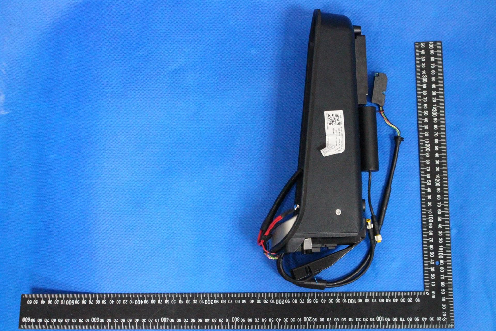
2ADEK-191230
Mar 21, 2020Holster
Equipment Class
DXX - Part 15 Low Power Communication Device Transmitter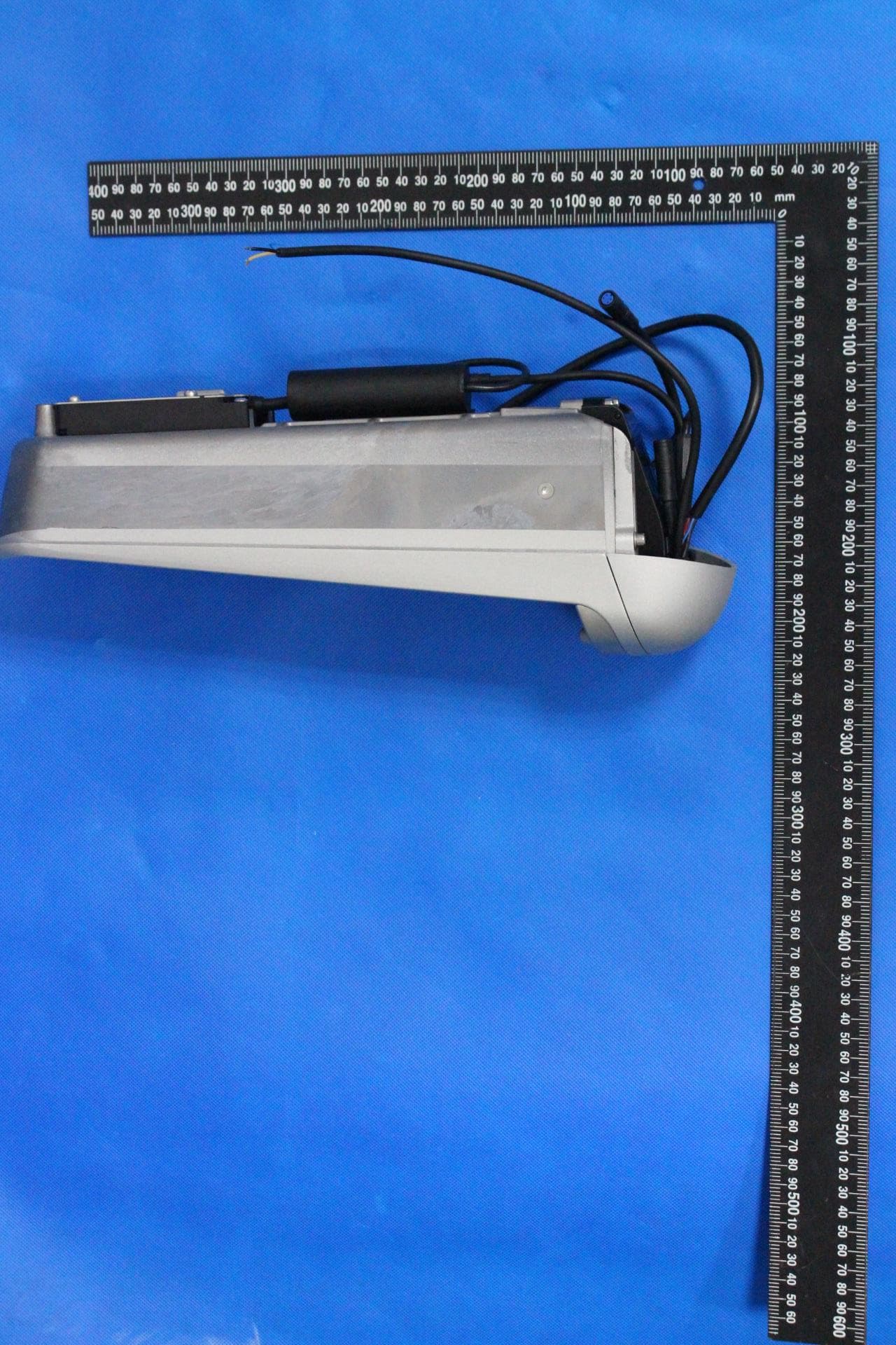
2ADEK-191220
Mar 21, 2020Holster
Equipment Class
DXX - Part 15 Low Power Communication Device Transmitter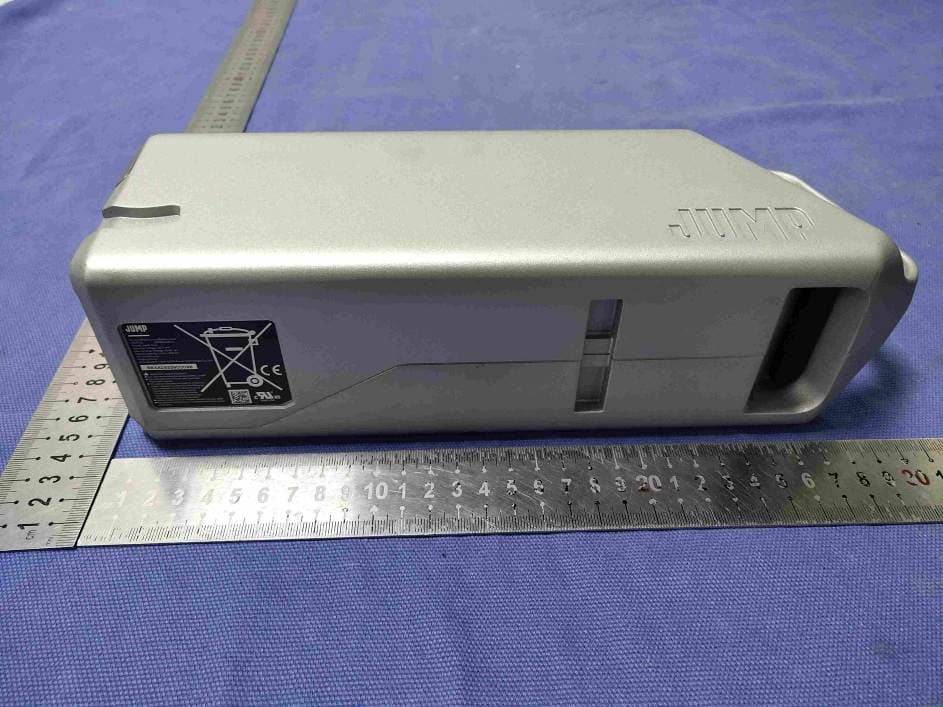
2ADEKJUMPPACK
Jan 06, 2020Rechargeable Li-ion Battery Pack
Equipment Class
DXX - Part 15 Low Power Communication Device Transmitter2ADEK102014SBP1
Nov 24, 2014SOBI Controller
Equipment Class
DXX - Part 15 Low Power Communication Device Transmitter