2AF6B-RAK3400Bluetooth module
Shenzhen RAKwireless Technology Co.,Ltd.
Click to zoom
Application Details
- Equipment Class
- DTS - Digital Transmission System
- Date of Grant
- Apr 24, 2021
- Application Purpose
- Original Equipment
- Date of Application
- Apr 24, 2021
- Equipment Note
- Bluetooth module
- Frequency Range
- 2402.00000000 - 2480.00000000
- Country
- China
Documents & Files
Document Text
Text extracted from the exhibit documents filed with the FCC. Open a document above to read the original.
Users Manual
RAK4630 1 RAK3400 LoRa Module WisDuo Series Version V1.0 | December 2020 R AK2011 RAK4630 2 Table of Contents 1Introduction.........................................................3 2Overview..............................................................3 2.1General description.............................................................................................3 2.2Main Features......................................................................................................3 2.3Block Diagram......................................................................................................4 2.4Pin Assignment.....................................................................................................5 2.5Pin Description.....................................................................................................6 2.6Power Consumption............................................................................................7 2.7Absolute Maximum Ratings................................................................................7 2.8Recommended operating conditions...................................................................8 3Mechanical Dimensions......................................9 3.1Top and Side Dimensions....................................................................................9 3.2Recommended Footprint....................................................................................9 4Recommended Reflow Profile..........................10 RAK4630 3 1Introduction This document defines RAK3400 module and describes hardware interface which are connected with customers applications. This document helps customers quickly understand the interface specifications, electrical and mechanical details, as well as other related information of RAK3400. 2Overview 2.1General description RAK3400 is an BLE5.0 wireless communication module, it includes an nRF52840, Ultra-low power consumption of 2.0uA in sleep mode, and BLE output power up to 4dBm. The module supports BLE 5.0. Its RF communication capabilities make it suitable for a variety of applications in the IoT field. 2.2Main Features □Compact Form Factor: 15 x 23 x 3 mm □44 Pin Stamp Pad for PCB SMT mounting □I/O ports: UART/I2C/GPIO/USB/SPI (optional NFC interface) □Temperature range: -40°C to +85°C □Supply voltage: 2.0 ~ 3.6V □Ultra-Low Power Consumption 2.0uA in sleep mode □BLE5.0 (Tx power -20 to +4 dBm in 4dB steps) R AK2011 RAK4630 4 R AK2011 2.3Block Diagram The following figure shows a block diagram of RAK3400. Figure 1: Block Diagram RAK4630 5 R AK2011 2.4Pin Assignment The following figure shows the pin assignment of RAK3400 module. Figure 2: Pin Assignment □NOTES □For single 3.3V power supply, connect VBAT_NRF, VDD_NRF, together with 3.3V power □For 3.6V li-SOCL2 battery or 4.2V li-MnO2 battery, connect VBAT_NRF with battery output, VDD_NRF can use to indicate IO voltage level. Please don’t power any chip with VDD_NRF. □GND pins should be connected to ground in the design. □VBAT_SX, VBAT_SX_IO is reserved, they are not connected to any chips in RAK3400 module. RAK4630 6 2.5Pin Description The following tables show the pin definition and description of RAK3400. Table 2: Definition of I/O Parameters TypeDescription PIPower Input POPower Output DIDigital Input DODigital Output IOBidirectional AIAnalog Input AOAnalog Output Table 3: Pin Description Power Supply Pin NamePin No.TypeDescriptionComment VDD_NRF43PIPower supply VBAT_NRF44PIHigh Power supply GND 14,16, 22,35, 36,38, 42 Ground I2C Interface Pin NamePin No.TypeDescriptionComment I2C1_SDA4IOI2C serial dataP0.13 I2C1_SCL5ODI2C serial clockP0.14 I2C2_SDA23IOI2C serial dataP0.24 I2C2_SCL24ODI2C serial clockP0.25 USB Interface Pin NamePin No.TypeDescriptionComment VBUS1PIUSB power5V input for 3.3V regulator USB_DP3IOUSB differential data(+) USB_DM2IOUSB differential data(-) UART Interface Pin NamePin No.TypeDescriptionComment UART1_TX 10DOUART1 transmitP0.20 UART1_RX 9DIUART1 receiveP0.19 UART1_DE 11DIUART1 detectP0.21 UART2_TX 7DOUART2 transmitP0.16 UART2_RX 6DIUART2 receiveP0.15 UART2_DE 8DIUART2 detectP0.17 Quad SPI Interface Pin NamePin No.TypeDescriptionComment SPI_CLK29DOSPI clockP0.03 SPI_CS34DOSPI chip selectP0.26 SPI_DIO033IOSPI data input/output 0P0.30 SPI_DIO132IOSPI data input/output 1P0.29 SPI_DIO231IOSPI data input/output 2P0.28 SPI_DIO330IOSPI data input/output 3P0.02 R AK2011 RAK4630 7 SWD Interface Pin NamePin No.TypeDescriptionComment SWDIO19Debug SWD I/O for debug and programming SWCLK18Debug SWD clock input for debug and programming RESET Pin NamePin No.TypeDescriptionComment RESET17DIReset the module NFC Interface Pin NamePin No.TypeDescriptionComment NFC113DINFC input 1P0.09 NFC212DINFC input 2P0.10 Antenna Interface Pin NamePin No.TypeDescriptionComment RF_BT15IOBluetooth antenna interface 50Ω Impedance If unused, keep this pin open GPIO Interface Pin NamePin No.TypeDescriptionComment GPIO P1.0125IOGeneral-purpose input/output GPIO P1.0226IOGeneral-purpose input/output GPIO P1.0327IOGeneral-purpose input/output GPIO P1.0428IOGeneral-purpose input/output ADC Interface Pin NamePin No.TypeDescriptionComment GPIO P0.31 / AIN7 39IO / AIGeneral-purpose IO / General purpose ADC interface GPIO P0.05 / AIN3 40IO / AIGeneral-purpose IO / General purpose ADC interface GPIO P0.04 / AIN7 41IO / AIGeneral-purpose IO / General purpose ADC interface 2.6Power Consumption The following table show the power consumption. Table 4: Power Consumption ItemPower ConsumptionCondition Tx mode BT@4dBm9mABT Tx mode Rx mode [email protected] Rx mode Sleep mode2.0uABT sleep 2.7Absolute Maximum Ratings R AK2011 R AK2011 RAK4630 8 The following table show the absolute maximum ratings of RAK3400 Table 5: Absolute Maximum Ratings SymbolDescriptionMin.Nom.Max.Unit VDD_NRFMCU power supply-0.3-3.9V VBUSUSB supply voltage-0.3-5.8V VBAT_NRFMCU high voltage power supply-0.3-5.8V ESD HBMHuman Body Model--2000V ESD CDMCharged Device Model--500V 2.8Recomm…
Text truncated - open the document above for the full version.
Users Manual
1 RA K20 11 RAK3401 1 RAK3401 Breakout Module WisCore-LoRa Series Version V1.0 | December 2020 2 RA K20 11 RAK3401 2 Table of Contents 1Introduction........................................................................................................................................3 2Overview..............................................................................................................................................3 General description......................................................................................................................3 2.13 2.2Main Features..............................................................................................................................3 2.3Board Realistic View...................................................................................................................4 2.4RAK3401 Mounting Sketch........................................................................................................4 2.5Schematic Diagram.....................................................................................................................4 2.5.1WisConnector.................................................................................................................5 2.5.2WisConnector pin order..................................................................................................5 2.5.3Core module....................................................................................................................5 2.5.4SWD interface.................................................................................................................6 2.5.5Power up automatic reset................................................................................................6 2.5.6Flash Memory.................................................................................................................7 2.6Absolute Maximum Ratings........................................................................................................7 2.7Recommended operating conditions...........................................................................................8 3Mechanical Dimensions......................................................................................................................8 Figure Index Figure 1: RAK3401’s top layer (left), and bottom layer (right)..............................................................4 Figure 2: RAK3401 mounting sketch........................................................................................................4 Figure 3: WisConnector pin definition......................................................................................................5 Figure 4: WisConnector pin order.............................................................................................................5 Figure 5: Cora module pin definition........................................................................................................6 Figure 6: SWD interface............................................................................................................................6 Figure 7: Power up automatic reset...........................................................................................................7 Figure 8: Flash Memory............................................................................................................................7 Figure 9: Mechanical Dimensions.............................................................................................................8 3 RA K20 11 RAK3401 3 1Introduction This document explains the design of the RAK3401 module and describes a hardware interface that is important to understand in order to build customized applications. This document helps customers quickly to understand the interface specifications, electrical and mechanical details, as well as other relevant information of RAK3401 module. 2Overview 2.1General description The RAK3401 module is part of the WisBlock series, specifically, it’s one of the modules that belong to the WisCore category. The RAK3401 is a breakout module designed to work with RAK5005 baseboard. Essentially, it is a RAK3400 stamp module with an expansion PCB and connectors compatible with the RAK5005 baseboard. It allows an easy way to access to the pins of the RAK3400 module in order to simplify development and testing processes. The module itself comprises a RAK3400 as its main component. The RAK3400 is a combination of a nRF52840 MCU, it features ultra-low power consumption of 2.0uA during sleep mode, and the BLE interface with output power up to 4dBm. The RF communication characteristic of the module (BLE) makes it suitable for a variety of applications in the IoT field such as home automation, sensor networks, building automation, personal area networks applications (health/fitness sensors, and monitors, etc.). 2.2Main Features I/O ports: UART/I2C/GPIO/USB/SPI (optional NFC interface) Temperature range: -40°C to +85°C Supply voltage: 2.0 ~ 3.6V Ultra-Low Power Consumption 2.0uA in sleep mode BLE5.0 (Tx power -20 to +4dBm in 4dB steps) Serial Wire Debug (SWD) interface Module size: 20 x 30mm 4 RA K20 11 RAK3401 4 2.3Board Realistic View Figure 1: RAK3401’s top layer (left), and bottom layer (right). 2.4RAK3401 Mounting Sketch The RAK3401 module is designed to work with the RAK5505 baseboard. Figure 2 shows how a RAK3401 module should be mounted on top of the RAK5505. Figure 2: RAK3401 mounting sketch. 2.5Schematic Diagram The following chapters will describe the breakout module schematic. It includes WisConnector, core module, SWD interface, power up automatic reset, and memory flash. 5 RA K20 11 RAK3401 5 2.5.1WisConnector The breakout module allows the RAK3400 stamp module’s pinout to be transferred to board-to-board connector, Figure 3 shows the definition of this connector. Figure 3: WisConnector pin definition. 2.5.2WisConne…
Text truncated - open the document above for the full version.
Cover Letter(s)
QF094234 Page 1 of 1 Revision 0 Authority to Act as Agent Date: 2021.04.01 TUV Rheinland Group 762 Park Avenue Youngsville, NC 27596 To Whom It May Concern: I appoint TUV Rheinland (Shenzhen) Co., Ltd. to act as our agent in the preparation of this application for equipment certification. I certify that submitted documents properly describe the device or system for which equipment certification is sought. I also certify that each unit manufactured, imported or marketed, as defined in the FCC or Industry Canada’s regulations will have affixed to it a label identical to that submitted for approval with this application. For instances where our authorized agent signs the application for certification on our behalf, I acknowledge that all responsibility for complying with the terms and conditions for Certification, as specified by TUV Rheinland Group, still resides with Shenzhen Rakwireless Technology Co., Ltd. / Room 506, Tsinghua Harbor, Science and Technology Park North Buildings, Nanshan District, Shenzhen, China For TCB applications, We certify that we are not subject to denial of federal benefits, that includes FCC benefits, pursuant to Section 5301 of the Anti-Drug Abuse Act of 1988, 21 U.S.C. 862. Further, no party, as defined in 47 CFR 1.2002 (b), to the application is subject to denial of federal benefits, that includes FCC benefits. Thank you, Agency Agreement Expiration Date: 12 months By : Vivian Xu (Signature) (Print Name) Title : Engineer Telephone : 19926584202 On behalf of : Shenzhen Rakwireless Technology Co., Ltd. (Company Name)
Cover Letter(s)
Confidentiality Letter Date: 2021-04-01 Subject: Confidentiality Request for FCC ID: 2AF6B-RAK3400 and IC ID: 25908-RAK3400 Pursuant to FCC 47 CRF 0.457(d) and 0.459 and IC RSP-100, Section 10, the applicant requests that a part of the subject FCC/IC application be held confidential. Type of Confidentiality Requested Exhibit Short Term Permanent Block Diagrams Short Term External Photos Short Term Permanent Internal Photos Short Term Permanent Operation Description/Theory of Operation Short Term Permanent Part List/Tune-Up Procedure Short Term Permanent Schematics Short Term Test Setup Photos Short Term Permanent User’s Manual Shenzhen Rakwireless Technology Co., Ltd. has spent substantial effort in developing this product and it is one of the first of its kind in industry. Having the subject information easily available to "competition" would negate the advantage they have achieved by developing this product. Not protecting the details of the design will result in financial hardship. Permanent Confidentiality: The applicant requests the exhibits listed above as permanently confidential be permanently withheld from public review due to materials that contain trade secrets and proprietary information not customarily released to the public. Short-Term Confidentiality: The applicant requests the exhibits selected above as short term confidential be withheld from public view for a period of 180 days from the date of the Grant of Equipment Authorization and prior to marketing. This is to avoid premature release of sensitive information prior to marketing or release of the product to the public. Applicant is also aware that they are responsible to notify TUV Rheinland in the event information regarding the product or the product is made available to the public. TUV Rheinland will then release the documents listed above for public disclosure pursuant to FCC Public Notice DA 04- 1705. Sincerely, By: Vivian Xu (Signature/Title) (Print name)
Cover Letter(s)
Date: 2021-02-25 FCC ID:2AF6B-RAK3400 IC: 25908-RAK3400 Type of Module: Single Modular Transmitter No. Requirements Device Conditions Comply (Y/N) 1 The radio elements of the modular transmitter must have their own shielding. The physical crystal and tuning capacitors may be located external to the shielded radio elements. The module has its own RF shielding. Refer to the external photos. Y 2 The modular transmitter must have buffered modulation/data inputs (if such inputs are provided) to ensure that the module will comply with part 15 requirements under conditions of excessive data rates or over-modulation. The EUT has buffered modulation/data inputs. It’s integrated on the chipset IC U3 / NRF52840. Refer to the schematics diagram. Y 3 The modular transmitter must have its own power supply regulation. The module has its own power supply regulation. Y 4 The modular transmitter must comply with the antenna and transmission system requirements of §§15.203, 15.204(b) and 15.204(c). The antenna must either be permanently attached or employ a “unique” antenna coupler. The antenna is IPEX antenna and antenna gain is 1.68dBi. Y 5 The modular transmitter must be tested in a stand- alone configuration, i.e., the module must not be inside another device during testing for compliance with part 15 requirements. The modular transmitter was tested in a stand-alone configuration via a laptop PC USB interface. Y 6 The modular transmitter must be equipped with either a permanently affixed label or must be capable of electronically displaying its FCC identification number. FCC ID is permanently on the PCB. Refer to the Label Location and Label. Y 7 The modular transmitter must comply with any specific rules or operating requirements that ordinarily apply to a complete transmitter and the manufacturer must provide adequate instructions along with the module to explain any such requirements. A copy of these instructions must be included in the application for equipment authorization. The User Manual instruction that the OEM how to use the label. Y 8 The modular transmitter must comply with any applicable RF exposure requirements in its final configuration. Refer to the test report. Y If you have any questions regarding this, please don’t hesitate to contact us. Sincerely, _________________________ (Vivian Xu / engineer) Shenzhen Rakwireless Technology Co., Ltd.
External Photos
Model RAK3400: ony the green PCB Model RAK3401: the green PCB + black PCB, the black PCB is a I/O extend for green RAK3400
Internal Photos
Model: RAK3401 Model: RAK3400
RF Exposure Info
Produkte Products Prüfbericht - Nr.: Test Report No. CN21UVL1 001 Seite 21 von 22 Page 21 of 22 6Safety Human Exposure 6.1Radio Frequency Exposure Compliance 6.1.1Electromagnetic Fields RESULT:Pass Test Specification Test standard:FCC KDB Publication 447498 v06 CFR47 FCC Part 2: Section 2.1093 CFR47 FCC Part 1: Section 1.1310 RSS-102 Issue 5 March 2015 Measurement Record: The measured maximum conducted output power of the EUT is 3.6dBm ≈ 2.29mW, which is far below the SAR exclusion threshold level 10mW (SAR Test Exclusion Thresholds for 100 MHz – 6 GHz and ≤ 50 mm), hence the EUT is excluded from SAR evaluation according to FCC KDB publication 447498 D01: Mobile and Portable RF Exposure. Guidance v06. The measured maximum specified e.i.r.p of the EUT is 5.28dBm ≈ 3.37mW, which is far below the SAR exclusion threshold level 4mW, hence the EUT is excluded from SAR evaluation according to RSS-102 Issue 5 section 2.5.1.
Test Report
Prüfbericht - Produkte Test Report - Products Prüfbericht-Nr.: Test report no.: CN21UVL1 001 Auftrags-Nr.: Order no.: 168304727 Seite 1 von 22 Page 1 of 22 Kunden-Referenz-Nr.: Client reference no.: N/A Auftragsdatum: Order date: 2021-01-19 Auftraggeber: Client: Shenzhen Rakwireless Technology Co., Ltd. Room 506, Bldg B, New Compark, Pingshan First Road, Taoyuan Street, XiLi town Nanshan District, Shenzhen, Guangdong, P.R. China Prüfgegenstand: Test item: WisDuo Bezeichnung / Typ-Nr.: Identification / Type no.: RAK3400, RAK3401 Auftrags-Inhalt: Order content: FCC and IC approval Prüfgrundlage: Test specification: CFR47 FCC Part 15: Subpart C Section 15.247 CFR47 FCC Part 15: Subpart C Section 15.207 CFR47 FCC Part 15: Subpart C Section 15.209 CFR47 FCC Part 2.1093 RSS-247 Issue 2 February 2017 RSS-Gen Issue 5 March 2019 RSS-102 Issue 5 March 2015 Wareneingangsdatum: Date of sample receipt: 2021-01-21 Please refer to photo documents Prüfmuster-Nr.: Test sample no.: A002990607-001 to 008 Prüfzeitraum: Testing period: 2021-01-22 – 2021-02-23 Ort der Prüfung: Place of testing: TÜV Rheinland (Shenzhen) Co., Ltd. Prüflaboratorium: Testing laboratory: TÜV Rheinland (Shenzhen) Co., Ltd. Prüfergebnis*: Test result*: Pass geprüft von: tested by: X Signed by: Alex Lan genehmigt von: authorized by: X Signed by: Winnie Hou Datum: Date: 2021-04-20 Ausstellungsdatum: Issue date: 2021-04-20 Stellung / Position Senior Project Engineer Stellung / Position Department Manager Sonstiges / Other: FCC ID: 2AF6B-RAK3400 IC: 25908-RAK3400 HVIN: RAK3400, RAK3401 Zustand des Prüfgegenstandes bei Anlieferung: Condition of the test item at delivery: Prüfmuster vollständig und unbeschädigt Test item complete and undamaged: * Legende: 1 = sehr gut 2 = gut 3 = befriedigend 4 = ausreichend 5 = mangelhalt P(ass) = entspricht o.g. Prüfgrundlage(n) F(ail) = entspricht nicht o.g. Prüfgrundlage(n) N/A = nicht anwendbar N/T = nicht getestet Legend: 1 = very good 2 = good 3 = satisfactory 4 = sufficient 5 = poor P(ass) = passed a.m. test specifications(s) F(ail) = failed a.m. test specifications(s) N/A = not applicable N/T = not tested Dieser Prüfbericht bezieht sich nur auf das o.g. Prüfmuster und darf ohne Genehmigung der Prüfstelle nicht auszugsweise vervielfältigt werden. Dieser Bericht berechtigt nicht zur Verwendung eines Prüfzeichens. This test report only relates to the a. m. test sample. Without permission of the test center this test report is not permitted to be V05 duplicated in extracts. This test report does not entitle to carry any test mark. TÜV Rheinland (Shenzhen) Co., Ltd. 1601 R&D Room, 1602-1604, 17-18F, Building 7 Site C, Vanke Cloud City Phase I, Xingke First Street, Xili Street, Xili Community, Nanshan District, Shenzhen 518052, P.R. China Mail: [email protected] · Web: www.tuv.com Produkte Products Prüfbericht - Nr.: Test Report No. CN21UVL1 001 Seite 2 von 22 Page 2 of 22 Test Summary 5.1.1 ANTENNA REQUIREMENT RESULT: Pass 5.1.2 MAXIMUM PEAK CONDUCTED OUTPUT POWER RESULT: Pass 5.1.3 CONDUCTED POWER SPECTRAL DENSITY RESULT: Pass 5.1.4 99%DB BANDWIDTH RESULT: Pass 5.1.5 6DB BANDWIDTH RESULT: Pass 5.1.6 CONDUCTED SPURIOUS EMISSIONS MEASURED IN 100 KHZ BANDWIDTH RESULT: Pass 5.1.7 RADIATED SPURIOUS EMISSION RESULT: Pass 5.1.8 CONDUCTED EMISSION ON AC MAINS RESULT: Pass 6.1.1 ELECTROMAGNETIC FIELDS RESULT: Pass Produkte Products Prüfbericht - Nr.: Test Report No. CN21UVL1 001 Seite 3 von 22 Page 3 of 22 Contents 1 GENERAL REMARKS ........................................................................................................................... 4 1.1 COMPLEMENTARY MATERIALS ............................................................................................................ 4 2 TEST SITES ........................................................................................................................................ 4 2.1 TEST FACILITIES ................................................................................................................................. 4 2.2 LIST OF TEST AND MEASUREMENT INSTRUMENTS................................................................................. 5 2.3 TRACEABILITY .................................................................................................................................... 7 2.4 CALIBRATION ..................................................................................................................................... 7 2.5 MEASUREMENT UNCERTAINTY............................................................................................................. 7 2.6 LOCATION OF ORIGINAL DATA ............................................................................................................. 7 2.7 STATUS OF FACILITY USED FOR TESTING ............................................................................................. 7 3 GENERAL PRODUCT INFORMATION ...................................................................................................... 8 3.1 PRODUCT FUNCTION AND INTENDED USE ............................................................................................. 8 3.2 RATINGS AND SYSTEM DETAILS .......................................................................................................... 8 3.3 INDEPENDENT OPERATION MODES ...................................................................................................... 9 3.4 NOISE GENERATING AND NOISE SUPPRESSING PARTS ......................................................................... 9 3.5 SUBMITTED DOCUMENTS..................................................................................................................... 9 4 TEST SET-UP AND OPERATION MODES ..............................................................................................10 4.1 PRINCIPLE OF CONFIGURATION SELECTION .......................................................................................10 4.2 TEST OPERATION AND TEST SO…
Text truncated - open the document above for the full version.
Test Setup Photos
Produkte Products Appendix A CN21UVL1 001 Page 1 of 3 Appendix A: Photographs of the Test Set-Up APPENDIX A: PHOTOGRAPHS OF THE TEST SET-UP.......................................................................................................1 PHOTOGRAPH 1: SET-UP FOR RADIATED SPURIOUS EMISSION, BELOW 1GHZ....................................................................................2 PHOTOGRAPH 2: SET-UP FOR RADIATED SPURIOUS EMISSION, ABOVE 1GHZ....................................................................................2 PHOTOGRAPH 3: SET-UP FOR CONDUCTED EMISSIONS ON AC MIANS.............................................................................................3 Produkte Products Appendix A CN21UVL1 001 Page 2 of 3 Photograph 1: Set-up for Radiated Spurious Emission, Below 1GHz Photograph 2: Set-up for Radiated Spurious Emission, Above 1GHz Produkte Products Appendix A CN21UVL1 001 Page 3 of 3 Photograph 3: Set-up for Conducted Emissions ON AC mians
Contact Information
Applicant
Vivian Xu(Engineer)
Technical Contact
Test Firm
TUV Rheinland (Shenzhen) Co., Ltd.Gina Yang
[email protected]86 755 8268 1497
Technical Specifications
| # | Rule Parts | Frequency Range | Power Output |
|---|---|---|---|
| 1 | 15C | 2.40 GHz - 2.48 GHz | 2.29 mW |
Other Applications from Shenzhen RAKwireless Technology Co.,Ltd.
2AF6B-13302
Aug 01, 2026Wisblock Wireless
Equipment Class
DTS - Digital Transmission System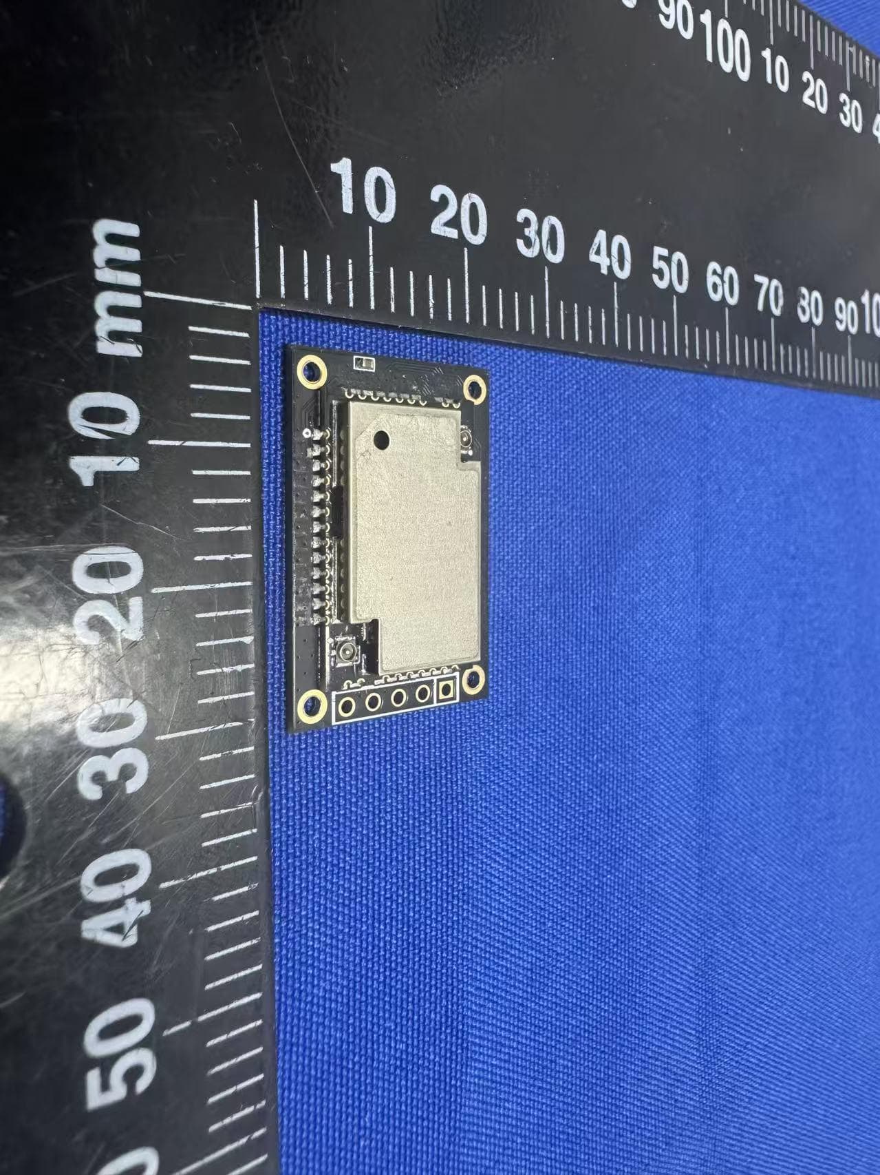
2AF6B-3112
Mar 09, 2026WisDuo Module
Equipment Class
DSS - Part 15 Spread Spectrum Transmitter
2AF6B-5167
Feb 04, 2026WisLink Module
Equipment Class
DTS - Digital Transmission System2AF6B-RAK7437
Jan 16, 2026WisGate X Industrial
Equipment Class
DTS - Digital Transmission System2AF6B-RAK7437C
Jan 16, 2026WisGate X Industrial
Equipment Class
JAB - Part 15 Class B Digital Device