2AJYU-8PYA004LTE /HSPA/GSM/GNSS MODULE
SIMCom Wireless Solutions Limited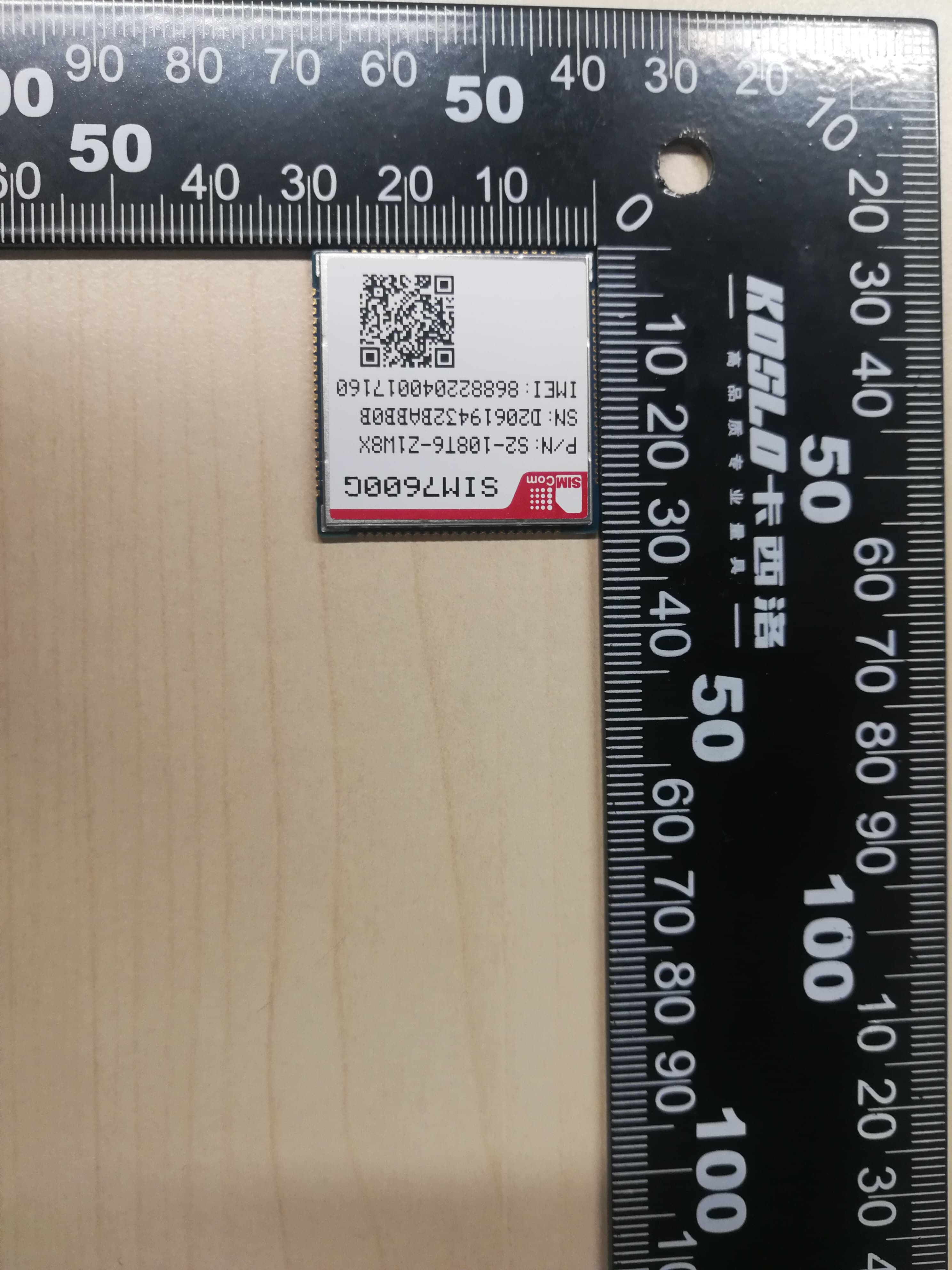
Click to zoom
Application Details
- Equipment Class
- PCB - PCS Licensed Transmitter
- Date of Grant
- Mar 11, 2020
- Application Purpose
- Original Equipment
- Date of Application
- Mar 11, 2020
- Equipment Note
- LTE /HSPA/GSM/GNSS MODULE
- Frequency Range
- 1710.70000000 - 1755.00000000
- Country
- China
Documents & Files
Document Text
Text extracted from the exhibit documents filed with the FCC. Open a document above to read the original.
Users Manual
SIM7600G/G-H_Hardware Design_V1.01 Smart Machine Smart Decision SIM7600G_SIM7600G-H_Hardware Design _V1.01 2 2019-10-21 Document Title SIM7600G/SIM7600G-H_Hardware Design Version 1.01 Date 2019-10-21 Status Released Document Control ID SIM7600G_SIM7600G-H_Hardware Design _V1.01 General Notes SIMCom offers this information as a service to its users to support the application and engineering efforts that use the products designed by SIMCom. The information provided is based on the requirements specifically from the users. SIMCom has not undertaken any independent search for additional relevant information, including any information that may be in the user’s possession. Furthermore, the system validation of the product designed by SIMCom within a larger electronic system remains the responsibility of the user or the user’s system integrator. All specifications supplied herein are subject to change without notice. Copyright This document contains the proprietary technical information which is the property of SIMCom Limited, copying of this document, giving it to others, the using or communication of the contents thereof are forbidden without the official authority by SIMCom. Offenders are liable to the payment of the damages. All rights are reserved in the event of grant of a patent or the registration of a utility model or design. All specifications supplied herein are subject to change without notice Copyright © SIMCom Wireless Solutions Co., Ltd. 2019 Smart Machine Smart Decision FCC Caution: (1)Exposure to Radio Frequency Radiation. This equipment must be installed and operated in accordance with provided instructions and the antenna(s) used for this transmitter must be installed to provide a separation distance of at least 20 cm from all persons and must not be collocated or operating in conjunction with any other antenna or transmitter. End-users and installers must be provided with antenna installation instructions and transmitter operating conditions for satisfying RF exposure compliance. (2) Any changes or modifications not expressly approved by the grantee of this device could void the user's authority to operate the equipment. (3) This Transmitter must not be co-located or operating in conjunction with any other antenna or transmitter. (4) Changes or modifications to this unit not expressly approved by the party responsible for compliance could void the user authority to operate the equipment. (6) Labelling requirements:This device complies with part 15 of the FCC Rules. Operation is subject to the following two conditions: (1) This device may not cause harmful interference, and (2) this device must accept any interference received, including interference that may cause undesired operation. (6) if the host is marketed so that end users do not have straight forward commonly used methods for access to remove the module so that the FCC ID of the module is visible; then an additional permanent label referring to the enclosed module: Contains Transmitter Module FCC ID: 2AJYU-8PYA004 or Contains FCC ID: 2AJYU-8PYA004 must be used. This product is suitable for collocation internal and external antenna.Gain the scope of the reference is as follows: Smart Machine Smart Decision SIM7600G_SIM7600G-H_Hardware Design _V1.01 3 2019-10-21 Contents Contents .............................................................................................................................................3 Revision History ................................................................................................................................5 1 Introduction ................................................................................................................................6 1.1 Product Outline .....................................................................................................................6 1.2 Hardware Interface Overview ...............................................................................................7 1.3 Hardware Block Diagram......................................................................................................8 1.4 Functional Overview .............................................................................................................9 2 Package Information................................................................................................................ 11 2.1 Pin Assignment Overview ................................................................................................... 11 2.2 Pin Description ....................................................................................................................14 2.3 Mechanical Information ......................................................................................................19 2.4 Footprint Recommendation .................................................................................................20 3 Interface Application ...............................................................................................................21 3.1 Power Supply ......................................................................................................................21 3.1.1 Power Supply Design Guide ........................................................................................22 3.1.2 Recommended Power Supply Circuit ..........................................................................23 3.1.3 Voltage Monitor ............................................................................................................23 3.2 Power on/Power off/Reset Function ....................................................................................24 3.2.1 Power on .......................................................................................................................24 3.2.2 Power off ......................................................................................................................25 3.2.3 Re…
Text truncated - open the document above for the full version.
Users Manual
Smart Machine Smart Decision SIM7600G_SIM7600G-H_Hardware Design _V1.01 51 2019-10-21 Figure 266: Antenna matching circuit (AUX_ANT) In above figure, R3, C3, C4 and R4 are used for auxiliary antenna matching. By default, the R3, R4 are 0Ωresistors, and the C3, C4 are reserved for tuning. D2 is a TVS for ESD protection, and it is optional for users according to application environment. Two TVS are recommended in the table below. Table 22: Recommended TVS Package Part Number Vender 0201 LXES03AAA1-154 Murata 0402 LXES15AAA1-153 Murata Note:SIMCom suggests the LTE auxiliary antenna to be kept on, since there are many high bands in the designing of LTE-TDD, such as band38, band40 and band41. Because of the high insert loss of the RF cable and layout lines, the receiver sensitivity of these bands above will have risk to meet the authentication without the diversity antenna. For more details about auxiliary antenna design notice, please refer to document [25]. 4.3 GNSS MODULE merges GNSS (GPS/GLONASS/BD) satellite and network information to provide a high-availability solution that offers industry-leading accuracy and performance. This solution performs well, even in very challenging environmental conditions where conventional GNSS receivers fail, and provides a platform to enable wireless operators to address both location-based services and emergency mandates. Smart Machine Smart Decision SIM7600G_SIM7600G-H_Hardware Design _V1.01 52 2019-10-21 4.3.1 GNSS Technical specification Tracking sensitivity: -159 dBm(GPS)/-158 dBm(GLONASS)/-159 dBm(BD) Cold-start sensitivity: -148 dBm Accuracy (Open Sky): 2.5m (CEP50) TTFF (Open Sky) : Hot start <1s, Cold start<35s Receiver Type: 16-channel, C/A Code GPS L1 Frequency: 1575.42±1.023MHz GLONASS: 1597.5~1605.8 MHz BD: 1559.05~1563.14 MHz Update rate: Default 1 Hz GNSS data format: NMEA-0183 GNSS Current consumption : 100mA (GSM/UMTS/LTE Sleep ,in total on VBAT pins) GNSS antenna: Passive/Active antenna Note: If the antenna is active type, the power should be given by main board because there is no power supply on the GPS antenna pad. If the antenna is passive, it is suggested that the external LNA should be used. 4.3.2 GNSS Application Guide Users can adopt an active antenna or a passive antenna to MODULE. If using a passive antenna, an external LNA is a must to get better performance. The following figures are the reference circuits. Figure 277: Active antenna circuit Smart Machine Smart Decision SIM7600G_SIM7600G-H_Hardware Design _V1.01 53 2019-10-21 Figure 288: Passive antenna circuit (Default) In above figures, the components C1, L1 and L2 are used for antenna matching. Usually, the values of the components can only be achieved after antenna tuning and usually provided by antenna vendor. C2 is used for DC blocking. L3 is the matching component of the external LNA, and the value of L3 is determined by the LNA characteristic and PCB layout. Both VDD of active antenna and V_LNA need external power supplies which should be considered according to active antenna and LNA characteristic. LDO/DCDC is recommended to get lower current consuming by shutting down active antennas and LNA when GNSS is not working. GNSS can be tested by NMEA port. NMEA sentences can be obtained through UART or USB automatically. NMEA sentences include GSV, GGA, RMC, GSA, and VTG. Before using GNSS, user should configure MODULE in proper operating mode by AT command. Please refer to related documents for details. MODULE can also get position location information through AT directly. Note: GNSS is closed by default and can be started by AT+CGPS. The AT command has two parameters, the first is on/off, and the second is GNSS mode. Default mode is standalone mode. AGPS mode needs more support from the mobile telecommunication network. Please refer to document [24] for more details. Smart Machine Smart Decision SIM7600G_SIM7600G-H_Hardware Design _V1.01 54 2019-10-21 5 Electrical Specifications 5.1 Absolute maximum ratings Absolute maximum rating for digital and analog pins of MODULE are listed in the following table: Table 23: Absolute maximum ratings Parameter Min. Typ. Max. Unit Voltage at VBAT -0.5 - 6.0 V Voltage at USB_VBUS -0.5 - 5.85 V Voltage at digital pins (RESET,SPI,Keypad,GPIO,I2C,UART,PCM) -0.3 - 2.1 V Voltage at digital pins (SD,USIM) -0.3 - 3.05 V Voltage at PWRKEY -0.3 - 1.8 5.2 Operating conditions Table 24: Recommended operating ratings Parameter Min. Typ. Max. Unit Voltage at VBAT 3.4 3.8 4.2 V Voltage at USB_VBUS 3.0 5.0 5.25 V Table 25: 1.8V Digital I/O characteristics* Parameter Description Min. Typ. Max. Unit V IH High-level input voltage 1.17 1.8 2.1 V V IL Low-level input voltage -0.3 0 0.63 V V OH High-level output voltage 1.35 - 1.8 V V OL Low-level output voltage 0 - 0.45 V I OH High-level output current(no pull down resistor) - 2 - mA I OL Low-level output current(no pull up resistor) - -2 - mA I IH Input high leakage current (no pull down resistor) - - 1 uA I IL Input low leakage current(no pull up resistor) -1 - - uA Smart Machine Smart Decision SIM7600G_SIM7600G-H_Hardware Design _V1.01 55 2019-10-21 *Note: These parameters are for digital interface pins, such as SPI, GPIOs (NETLIGHT, FLIGHTMODE, STATUS, USIM_DET, SD_DET), SDIO, I2C, UART, PCM, COEXn, and BOOT_CFG0. The operating temperature of MODULE is listed in the following table. Table 26: Operating temperature Parameter Min. Typ. Max. Unit Normal operation temperature -30 25 80 °C Extended operation temperature* -40 25 85 °C Storage temperature -45 25 +90 °C *Note: Module is able to make and receive voice calls, data calls, SMS and make GSM/ UMTX/LTE traffic in -40°C ~ +85°C. The performance will be reduced slightly from the 3GPP specifications if the temperature is outside the normal operating temperature range and still within the extreme operating temperature range. 5.3 Operating Mode 5.3.1 Operating Mode Definition The table below summarizes the various operating modes…
Text truncated - open the document above for the full version.
Cover Letter(s)
SCS-F18: Project and Product Certification Representative Authorization Letter Page 1 of 2 Rev 6.0 775 Montague Expressway Milpitas, CA 95035 Tel: 408-526-1188 Fax: 408-526-1088 Email: [email protected] Project and Product Certification Representative Authorization Letter Reason for Amendment (current / obsolete) Revision History Approved Date From To Initial Release (obsolete) 1.0 1.0 Nov-14-2006 Revised wording (obsolete) 1.0 2.0 Sept–25-2007 Updated company template (obsolete) 2.0 3.0 Jan-31-2012 Updated letter information (obsolete) 3.0 4.0 May-23-2014 Added FCC ID field (obsolete) 4.0 5.0 Sep-16-2014 Updated company name & logo (current) 5.0 6.0 Jun-27-2018 SCS-F18: Project and Product Certification Representative Authorization Letter Page 2 of 2 Rev 6.0 (Client's Company Letterhead / Logo) SIMCom Wireless Solutions Limited Logo:SIMCOM (3.10. 2020) To: BVCPS, INC. 775 Montague Expressway, Milpitas, CA 95035 USA Dear Sir/Madam, Re: Product Certification Representative Authorization Letter We, SIMCom Wireless Solutions Limited hereby authorize Bureau Veritas Consumer Product Services, Inc. to act as a Certification Body for certifying for the following project(s): FCC ID: 2AJYU-8PYA004 Product Description: LTE /HSPA/GSM/GNSS MODULE Model: SIM7600G /SIM7600G miniPCIE Sincerely, Client’s signature Client’s name / title Li yongsheng/Project manager Contact information / address: No.633 Jinzhong Road,Shanghai
Cover Letter(s)
SCS-F19: Confidentiality Request Letter Page 1 of 2 Rev 6.0 775 Montague Expressway Milpitas, CA 95035 Tel: 408-526-1188 Fax: 408-526-1088Email: [email protected] Confidentiality Request Letter Reason for Amendment (current / obsolete) Revision History Approved Date From To Initial Release (obsolete) 1.0 1.0 Nov-14-2006 Adding CFR 2.459 (obsolete) 1.0 2.0 August – 11 - 2008 Updated company template& Added text box (obsolete) 2.0 3.0 Jan-31-2012 Added IC confidentiality letter form (obsolete) 3.0 4.0 March-26-2015 Corrections to STC form. Added reference to KDB (obsolete) 4.0 5.0 Nov-19-2015 Updated company logo (current) 5.0 6.0 Jun-26-2019 SCS-F19: Confidentiality Request Letter Page 2 of 2 Rev 6.0 (Client's Company Letterhead / Logo) SIMCom Wireless Solutions Limited Logo:SIMCOM (3.8. 2020) To: Federal Communications Commission Authorization and Evaluation Division 7435 Oakland Mills Road Columbia, MD Subject: Permanent Confidentiality Request for FCC ID: 2AJYU-8PYA004 Pursuant to sections 0.457 and 0.459 of CFR 47, we respectfully request permanent confidential treatment of the following Exhibits accompanying this application as: - Block Diagram - Schematics - Operational Description - Tune up Procedure - Part List The above materials contain trade secrets and proprietary information not customarily released to the public. The public disclosure of these materials may be harmful to the applicant and provide unjustified benefits to its competitors. The applicant understands that disclosure of this application and all accompanying documentation will not be made before the date of the Grant for this application. Sincerely, Client’s signature: Client’s name & title: Li yongsheng/Project manager Contact information / address: No.633 Jinzhong Road,Shanghai
Cover Letter(s)
SCS-F26 Modular Approval Letter Page 1 of 2 Rev 12.0 775 Montague Expressway Milpitas, CA 95035 Tel: 408-526-1188 Fax: 408-526-1088 Email: [email protected] Modular Approval Declaration Letter Reason for Amendment (current / obsolete) Revision History Approved Date From To Initial Release (Obsolete) 1.0 1.0 Dec-04-2006 Added IC Modular Letter (Obsolete) 1.0 2.0 Feb 16 2009 Add LMA and MA option (Obsolete) 2.0 3.0 April 14 2010 Revised per RSS Gen issue 3.0 (Obsolete) 3.0 4.0 Jan 12 2011 Removed Foot(2) (obsolete) 4.0 5.0 July 19 2011 Adding New note per KDB996369 D01 V01R03 (obsolete) 5.0 6.0 August 29 2011 Updated company template & Added text box (obsolete) 6.0 7.0 Jan-31-2012 Updated modular requirement (obsolete) 7.0 8.0 Sept 05 2014 Updated template to meet RSP 100 issue 10 (obsolete) 8.0 9.0 Nov 20 2014 Updated template to meet RSP 100 issue 11 (obsolete)) 9.0 10.0 March 19 2015 Revised the Modular Requirement statements (obsolete) 10.0 11.0 July 28, 2016 Updated template with BV logo (current) 11.0 12.0 June 26, 2019 SCS-F26 Modular Approval Letter Page 2 of 2 Rev 12.0 SIMCom Wireless Solutions Limited (Date) 3/8/2020 (LTE /HSPA/GSM/GNSS MODULE) FCC ID: 2AJYU-8PYA004 , is seeking FCC Authorization as a Single Modular Transmitter / Single Limited Modular Transmitter (Please check one) The EUT meets the requirements for Single Modular Approval / Single Limited Modular Approval (Please check one) as detailed in KDB 996369. Compliance to each of the requirements is described below: Item Modular requirement Yes No Please provide a detailed explanation if the answer is “No.” 1 Have its own RF shielding Yes 2 Have buffered modulation/data inputs (if such inputs are provided) Yes 3 The modular transmitter must have its own power supply regulation. Yes 4 Meet the antenna requirements of section 15.203 Yes 5 Be tested in a stand-alone configuration, i.e., the antenna, AC or DC power and data input/output lines must be connected to the module but, the module must not be inside another case during testing. Yes 6 Be labeled with its own FCC ID number, and if the FCC ID is not visible when the module is installed inside another device, then the outside of the device into which the module is installed must also display a label referring to the enclosed module. Yes 7 The modular transmitter is manufactured so that the user can not influence the operation of the transmitter that will operate outside of the scope of the regulations. Yes 8 Address compliance with the Commission`s RF exposure limits in Sections 1.1310 and 2.1093. Yes Note: (1) LMA may be granted when one or more of the requirements in the table above cannot be demonstrated. LMA will also be issued in those instances where applicants can demonstrate that they will retain control over the final installation of the device, such that compliance of the end product is assured. In such cases, an operating condition on the LMA for the module must state that the module is only approved for use when installed in devices produced by a specific manufacturer. When LMA is sought, the application for equipment certification must specifically state how control of the end product into which the module will be installed, and will be maintained, such that full compliance of the end product is always ensured. (2) Please provide Clear and specific instructions describing the conditions, limitations and procedures for third-parties to use and/or integrate the module into a host device. (3) For non-Software Defined Radio transmitter modules where software is used to ensure compliance of the device, technical description of how such control is implemented to ensure prevention of third party modification must be provided (see KDB 594280). Note 1: Compliance of a module in its final configuration is the responsibility of the applicant. A host device will not be considered certified if the instructions regarding antenna configuration provided in the original description, of one or more separately certified modules it contains, were not followed. Example: A separately certified low-power transceiver module using Bluetooth technology which is housed in a desktop computer, laptop or peripheral does not require the overall system to be recertified, if the desktop computer, laptop or peripheral, as a stand-alone unit, complies with all applicable technical standards. Client’s signature Client’s name / title Li yongsheng/Project manager Contact information / address : No.633 Jinzhong Road,Shanghai
Cover Letter(s)
SIMCom Wireless Solutions Limited Declaration Letter SIM7600G and SIM7600G miniPCIE are both LTE /HSPA/GSM/GNSS MODULE. They have the same software version and hardware design, including chipset, circuits, PCB and components. SIM7600G miniPCIE is combined with a SIM7600G module and a miniPCIE adapter board. The adapter board switches SIM7600G module to follow PCI Express Mini Card 1.2 standard connector protocol. No any other internal changes in SIM7600G module. Following details are the difference between two modules. Module Frequency bands Interface SIM7600G GSM:GSM850/PCS1900; WCDMA:B2 /4/5; LTE:B2/4/5/7/12/13/25/26/41/66; Only Module, LCC package SIM7600G miniPCIE GSM:GSM850/PCS1900; WCDMA:B2/4/5; LTE:B2/4/5/7/12/13/25/26/41/66; PCI Express Mini Card 1.2 standard connector Signature: Printedname/title: Address:No.633 Jinzhong Road,Shanghai external photo
External Photos
B19W50596 _External Photos EUT FRONT EUT BACK _main antenna port SIM7600G miniPCIE SIM7600G
ID Label/Location Info
B19W50598 _Label Photos SIM7600G SIM7600G miniPCIE
Internal Photos
B19W50596_InternalPhotos A ntenna Mainantennaport
RF Exposure Info
TEST REPORT REPORT NUMBER: B19W50598-MPE-Rev2 ON Type of Equipment: LTE /HSPA/GSM/GNSS MODULE Type of Designation: SIM7600G/SIM7600G miniPCIE Manufacturer: Simcom Wireless Solutions Limited FCC ID: 2AJYU-8PYA004 ACCORDING TO FCC CFR 47 Part 2.1091《Radiofrequency radiation exposure evaluation: mobile devices》 FCC CFR 47 Part1.1310《Radiofrequency radiation exposure limits》 Chongqing Academy of Information and Communication Technology Month date, year Feb, 26, 2020 Signature Zhang Yan Director Note: The test results in this test report relate only to the devices specified in this report. This report shall not be reproduced except in full without the written approval of Chongqing Academy of Information and Communications Technology. Report NO.:B19W50598-Rev2 Chongqing Academy of Information and Communication Technology Address:No. 8,Yuma Road, Chayuan New City, Nan’an District, Chongqing, P. R. China,401336 Tel: 0086-23-88069965 FAX:0086-23-88608777 Page 1of17 CONTENTS 1. TEST LABORATORY .................................................................................................................... 3 1.1. TESTING LOCATION ............................................................................................................ 3 1.2. TESTING ENVIRONMENT ................................................................................................... 3 1.3. PROJECT DATA ..................................................................................................................... 3 1.4. SIGNATURE ........................................................................................................................... 3 2. CLIENT INFORMATION ............................................................................................................... 4 2.1. APPLICANT INFORMATION ............................................................................................... 4 2.2. MANUFACTURER INFORMATION .................................................................................... 4 3. EQUIPMENT UNDER TEST (EUT) AND ANCILLARY EQUIPMENT (AE) ............................ 5 3.1. ABOUT EUT ........................................................................................................................... 5 3.2. INTERNAL IDENTIFICATION OF EUT USED DURING THE TEST ................................ 5 3.3. INTERNAL IDENTIFICATION OF AE USED DURING THE TEST .................................. 5 4. REFERENCE DOCUMENTS ......................................................................................................... 6 4.1. APPLICABLE STANDARDS ................................................................................................. 6 4.2. TEST LIMITS .......................................................................................................................... 6 5. TEST RESULTS .............................................................................................................................. 7 5.1. RF POWER OUTPUT ............................................................................................................. 7 5.2. CALCULATION INFORMATION ......................................................................................... 8 5.3. RESULTS................................................................................................................................. 8 5.4. RESULT OF GSM 850 ............................................................................................................ 9 5.5. RESULT OF GSM1900 ........................................................................................................... 9 5.6. RESULT OF GPRS 850 4TS ................................................................................................... 9 5.7. RESULT OF GRPS 1900 4TS ............................................................................................... 10 5.8. RESULT OF WCDMA BAND2 ............................................................................................ 10 5.9. RESULT OF WCDMA BAND4 ............................................................................................ 11 Report NO.:B19W50598-Rev2 Chongqing Academy of Information and Communication Technology Address:No. 8,Yuma Road, Chayuan New City, Nan’an District, Chongqing, P. R. China,401336 Tel: 0086-23-88069965 FAX:0086-23-88608777 Page 2of17 5.10. RESULT OF WCDMA BAND5 ............................................................................................ 11 5.11. RESULT OF LTE BAND2 ..................................................................................................... 12 5.12. RESULT OF LTE BAND4 ..................................................................................................... 12 5.13. RESULT OF LTE BAND5 ..................................................................................................... 12 5.14. RESULT OF LTE BAND7 ..................................................................................................... 13 5.15. RESULT OF LTE BAND12 ................................................................................................... 13 5.16. RESULT OF LTE BAND13 ................................................................................................... 14 5.17. RESULT OF LTE BAND25 ................................................................................................... 14 5.18. RESULT OF LTE BAND26 ................................................................................................... 14 5.19. RESULT OF LTE BAND41 ................................................................................................... 15 5.20. RESULT OF LTE BAND66 ................................................................................................... 15 ANNEX A: EUT PHOTOGRAPH ........................................................................................................ 17 Report NO.:B19W50598-Rev2 Chongqing Academy …
Text truncated - open the document above for the full version.
Test Report
TESTREPORT REPORTNUMBER:B19W50598-WWAN_Rev1 ON TypeofEquipment:LTE/HSPA/GSM/GNSSMODULE ModelName:SIM7600G/SIM7600GminiPCIE Manufacturer:SIMComWirelessSolutionsLimited ACCORDINGTO FCCCFRPart2,FREQUENCYALLOCATIONSANDRADIOTREATYMATTERS;GENERAL RULESANDREGULATIONS;e-CFR,Mar17,2015 PART22,PUBLICMOBILESERVICES,e-CFR,Mar17,2015 PART24,PERSONALCOMMUNICATIONSSERVICES,e-CFR,Mar17,2015 PART27,MISCELLANEOUSWIRELESSCOMMUNICATIONSSERVICES,e-CFR,Aug.15,2014 PART90,PRIVATELANDMOBILERADIOSERVICES,e-CFR,Jan.26,2012 RSS-Gen—GeneralRequirementsforComplianceofRadioApparatus.,November13,2014 RSS-130MobileBroadbandServices(MBS)EquipmentOperatingintheFrequencyBands698-756 MHzand777-787MHz,October2013 RSS-132—CellularTelephoneSystemsOperatingintheBands824-849MHzand869-894MHz,Issue 3,January2013 RSS-133—2GHzPersonalCommunicationsServices,Issue6,January2013 RSS-139—AdvancedWirelessServices(AWS)EquipmentOperatingintheBands1710-1780MHz and2110-2180MHz,Issue3,February2015 RSS-199BroadbandRadioService(BRS)EquipmentOperatingintheBand2500-2690MHz,Issue3, October2016 ChongqingAcademyofInformationandCommunicationsTechnology Monthdate,year Mar,10,2020 Signature ZhangYan Director ChongqingAcademyofInformationandCommunicationsTechnology ReportNo.:B19W50598-WWAN_Rev1 Address : No.8,YumaRoad,ChayuanNewCity,Nan’anDistrict,Chongqing,P.R.China,401336 Tel:0086-23-88069965FAX:0086-23-88608777 Page 1 of430 Note: Thetestresultsinthistestreportrelateonlytothedevicesspecifiedinthisreport.Thisreport shallnotbereproducedexceptinfullwithoutthewrittenapprovalofChongqingAcademyof InformationandCommunicationsTechnology. RevisionVersion ReportNumberRevisionDateMemo B19W50598V0.02020-03-07-- B19W50598V1.02020-03-10-- ChongqingAcademyofInformationandCommunicationsTechnology ReportNo.:B19W50598-WWAN_Rev1 Address : No.8,YumaRoad,ChayuanNewCity,Nan’anDistrict,Chongqing,P.R.China,401336 Tel:0086-23-88069965FAX:0086-23-88608777 Page 2 of430 FCCID:2AJYU-8PYA004 ISEDC:23761-8PYA005 ReportDate:2020-03-10 TestFirmName: ChongqingAcademyofInformationand CommunicationsTechnology FCCRegistrationNumber:CN1239 ISEDC:RegistrationNumber:11590A Statement Themeasurementsshowninthisreportweremadeinaccordancewiththeprocedures describedontestpages.Allreportedtestswerecarriedoutonasampleequipmentto demonstratelimitedcompliancewithFCCCFR47Parts2,22,24,27,90andRSS-Gen, 130,132,133,139and199,Thesampletestedwasfoundtocomplywiththe requirementsdefinedintheappliedrules. ChongqingAcademyofInformationandCommunicationsTechnology ReportNo.:B19W50598-WWAN_Rev1 Address : No.8,YumaRoad,ChayuanNewCity,Nan’anDistrict,Chongqing,P.R.China,401336 Tel:0086-23-88069965FAX:0086-23-88608777 Page 3 of430 CONTENTS 1GENERALINFORMATION.................................................................................................................................4 1.1NOTES..................................................................................................................................................................4 1.2TESTERS..............................................................................................................................................................5 1.3TESTINGLABORATORYINFORMATION....…
Text truncated - open the document above for the full version.
Contact Information
Applicant
Yongsheng Li(Manage)
Test Firm
Chongqing Academy of Information and CommuncationsLi Qiao
[email protected]023-88512631
Technical Specifications
| # | Rule Parts | Frequency Range | Power Output | Emission | Tolerance |
|---|---|---|---|---|---|
| 27 | 27 | 1.71 GHz - 1.75 GHz | 140.00 mW | 17M8G7D | 0.004 ppm |
Other Applications from SIMCom Wireless Solutions Limited
2AJYU-8XAC001
Jul 09, 2026LPWA Wireless Module
Equipment Class
PCB - PCS Licensed Transmitter2AJYU-8BM0002
Nov 26, 2025LTE Module
Equipment Class
PCB - PCS Licensed Transmitter2AJYU-8XRA002
Dec 14, 2023LTE Wireless Data Module
Equipment Class
NII - Unlicensed National Information Infrastructure TX
2AJYU-8XS0001
Nov 01, 2023SIM7672G
Equipment Class
TNB - Licensed Non-Broadcast Station Transmitter
2AJYU-8XK0002
Sep 13, 2023Wireless Data Module
Equipment Class
DSS - Part 15 Spread Spectrum Transmitter