2AND8-10WCALWireless Charging Alarm Clock
CJ Global Inc.
Click to zoom
Application Details
- Equipment Class
- 8CC - Part 18 Consumer Device
- Date of Grant
- Sep 02, 2020
- Application Purpose
- Original Equipment
- Date of Application
- Sep 02, 2020
- Equipment Note
- Wireless Charging Alarm Clock
- Frequency Range
- 0.11000000 - 0.20500000
- Company
- CJ Global Inc.
- Country
- United States
Documents & Files
Document Text
Text extracted from the exhibit documents filed with the FCC. Open a document above to read the original.
Users Manual
lOWATT Wireless Charging Alarm Clock ITEM 24714 USER MANUAL - ENGLISH Main Features 1. Time Display Mode: 12 or 24 hour time display 2. Calend「ar Mode: Display month and date 3. Alarm Mode: Triple alarm time setting 4. Temperature ure ure mode: Range from 0°C - 50°C (32°F - 122°F) 5. 3 Display Modes dp-7,dp-2 and dp-3 6. Power saving mode: Activate LED display by touch 7. Power supply: 3xAAA Batteries for LED display (not included) or USB Cable Included for the wireless charger function) CR2032 battery(included)to keep time memory FULL Screen Display PM Indicator Alarm Symbol Temperature Symbol Operating Instructions After power on, LED turns on with a beeping sound and will enter the time setting mode. Under time display mode, press the SET button to check below in sequence Time-> Calendar-> A 1 (Alarm 1), A2 (Alarm 2), A3 (Alarm 3) Time Setting 1. Under the Time Mode, press and hold the SET button for 2 seconds to set the clock. 2. Press the SET button repeatedly to set the time in the following sequence: 12124hr switch over「-> Hour-> Minute->Exit 3. Press the UP/ DOWN buttons to adjust the hour and minute digits. Press and hold the UP/ DOWN buttons to speed up the scanning of the digits. 4. When the 12-hour format 1s set, the PM indicator on the top left corner will appear in the afternoon 5. The setting mode will return to time display mode if there is no operation for 15seconds Date Setting 1. Under the Calendar Mode, press and hold the SET button for 2 seconds to set the date 2. Press the SET button repeatedly to set the date as the following sequence. Year - >month -> day->Exit 3. Press the UP/ DOWN buttons to adjust the year ,month and date Press and hold the UP/ DOWN buttons to speed the scanning of the digits 4. The setting mode will return to time display mode if there is no operation fo 「15 seconds Alarm Setting 3 different aIarm time settings a「e possible and you can store 3 different ala「m times 1n memory 1. Under the Alarm Mode A1, press the UP button to turn on the ala「m and press again to turn off 2. When A1 is activated,'oN A1' will appear on the display, quickly then it will Enter to alarm time display 3. Press the SET button for 2 seconds and the display will flash now you can set the alarm time 4. p「ess UP/DOWN buttons to adjust the alarm time. P「ess and hold the UP/DOWN button to speed up the scanning of the d1g1ts 5. When the Alarm is activated, the Alarm Symbol will turn on 6. The setting mode will exit f there is no operation for 15 seconds *A2 and A3 alarm can be set 1n the same way as A1 *Alarm will ring for 1 minute at the set time, p「ess any button to stop the alarm *Please note the alarm symbol will stay on and will ring the next day at the same time unless deactivated in the alarm settings Temperature Display *After the power is turned on, the clock will automatically detect the current room temperature and update the temperature every 60 seconds * Press the DOWN button for seconds to switch between Celsius(°C) and Fahrenheit(°F) OTHER FUNCTIONS Voice Activation / Touch Feature The Voice Activation feature will turn on the LED time and temperature reading when you make a noise (like a clap) o「 by touching the unit. Note this is a power saving mode that can be turned off if you want the display to show all the time Display Modes Under clock, calendar or temperature more, press the UP button to switch between Dp-7, Dp-2 and dP-3 display modes dp-1 mode: LED alternately displays time and date. Time will display for 10 seconds, date will display for 2 seconds For example: press the UP button to enter the dp-1 Mode, after setting 1t return back to time display. Under display mode, the LED display will alternate 1n the following sequence·-> time (10seconds)-> date(2seconds) dp-2 mode: Press the UP button to ente门hedp-2 mode, set you「 desired mode (Time, Date o「 Alarm)to keep this mode on the screen. For example Press the UP button to enter to the dp-2 mode, after settings are finished it return back to time display. If you always want to keep Time display showing, press the SET button to enter Time mode, the screen will keep Time display. If you always want to keep Date display showing, press the SET button to enter Date mode, the screen will keep the Date display If you always want to keep Alarm display showing, press the SET button to enter Alarm mode, the screen will keep the Alarm display dp-3 mode: Press the UP button to enter thedp-3 mode, under this mode , the screen default Time will always display after 15 seconds For example press the SET button to check Time->Date->Alarm as sequence, it will automatically return back to Time display after 15 seconds if there is no operation. Power saving and Touch control mode *The default mode is Sd (power saving off) Under Time Mode press the DOWN key to turn on the Power Saving Mode. The clock will then display ‘oN Sd’ DOWN again to turn off the Power Saving Mode.*Under Power Saving Mode, without any operation on For 30 seconds, the LED display will automatically turn off..*Unde「 Power Saving Mode touch the LED clock or touch the table to turn on the LED display.*Under power saving Mode when alarm is ringing the LED display will automatically turn on Built in Time Memory Built in CR2032 battery keeps the time running when power is off, but other functions cannot be used If time memory doesn'’t work anymore,please replace the built in CR2032 battery behind the battery compartment Specifications > n put: 5V 2A, 9V 1.5A >Output 5V1A,9V1A > Stand by Power「 <0 2W > Charging Distance:5-7 0 MM > Charging Effect 75% > Charging Power: 10 W > Power Supply USB 5V / 3*AAA battery case (battery not included) / button battery included for clock Package contents Wireless Cha「g1ng Alarm Clock x 7 Micro USB Power Cable x 1 FCC Statement This device complies with part 18 of the FCC Rules. Operation is Subject To the following two conditions: (1) This device may not cause harmful interference, and (2) this device must accept any inter…
Text truncated - open the document above for the full version.
Cover Letter(s)
CJ Global Inc. Agent Authorization Company: CJ Global Inc. Address: 20-21 Wagaraw Road Bldg 30 Fair Lawn, New Jersey, NJ 07410, United States Product Name: Wireless Charging Alarm Clock Trade Mark: N/A Model Number(s): 24714, 24057-DI, 24059-DI FCC ID: 2AND8-10WCAL We authorize MiCOM Labs Inc., 575 Boulder Court, Pleasanton, California 94566, USA, to act on our behalf on all matters concerning the certification of above named equipment. We declare that MiCOM Labs Inc. is allowed to forward all information related to the approval and certification of equipment to the regulatory agencies as required and to discuss any issues concerning the approval application. Any and all acts carried out by MiCOM Labs on our behalf shall have the same effect as acts of our own. Signature: Date: 2020-09-02 Name: Coby Chen Title: Manager Company: CJ Global Inc.
Cover Letter(s)
CJ Global Inc. Office of Engineering Technology Federal Communications Commission 7435 Oakland Mills Road Columbia, MD 21046 USA Dear Sir/Madam, We, CJ Global Inc. Hereby declares the following statement for FCC, PCB board, circuit, structure and internal of these model(s) are the same, Only model number is different for these model: Product Name: Wireless Charging Alarm Clock Model Number(s): 24714, 24057-DI, 24059-DI Sincerely, Signature: Date: 2020-09-02 Name: Coby Chen Title: Manager Company: CJ Global Inc.
Cover Letter(s)
CJ Global Inc. Office of Engineering Technology Federal Communications Commission 7435 Oakland Mills Road Columbia, MD 21046 USA Date: 2020-09-02 Subject; Request for Confidentiality FCC ID: 2AND8-10WCAL To Whom It May Concern, Pursuant to the provisions of the Commission’s rules Title 47 Sections §0.457 and §0.459, we are requesting the Commission to withhold the following attachment(s) as confidential documents from public disclosure indefinitely. These documents contain detailed system and equipment descriptions and are considered as proprietary information in operation of the equipment. The public disclosure of these documents might be harmful to our company and would give competitors an unfair advantage in the market. Schematic Diagram Block Diagram Operational Description In additional to above mentioned documents, in order to comply with the marketing regulations in Title 47 CFR §2.803 and the importation rules in Title 47 CFR §2.1204, while ensuring that business sensitive information remains confidential until the actual marketing of newly authorized devices, we request Short Term Confidentiality of the following attachment(s); External Photos Test Setup Photos Internal Photos User Manual For 45 days, pursuant to Public Notice DA 04-1705. OR For 180 days pursuant to KDB 726920 D01. It is our understanding that all measurement test reports, FCC ID label format and correspondence during the certification review process cannot be granted as confidential documents and this information will be available for public review once the grant of equipment authorization is issued. Sincerely, Signature: Name: Coby Chen Title: Manager
External Photos
SHENZHEN LCS COMPLIANCE TESTING LABORATORY LTD. FCC ID: 2AND8-10WCAL IC: 23749-10WCAL This report shall not be reproduced except in full, without the written approval of Shenzhen LCS Compliance Testing Laboratory Ltd. Page 1 of 4 1. EXTERIOR PHOTOGRAPHS Fig. 1 Fig. 2 SHENZHEN LCS COMPLIANCE TESTING LABORATORY LTD. FCC ID: 2AND8-10WCAL IC: 23749-10WCAL This report shall not be reproduced except in full, without the written approval of Shenzhen LCS Compliance Testing Laboratory Ltd. Page 2 of 4 Fig. 3 Fig. 4 SHENZHEN LCS COMPLIANCE TESTING LABORATORY LTD. FCC ID: 2AND8-10WCAL IC: 23749-10WCAL This report shall not be reproduced except in full, without the written approval of Shenzhen LCS Compliance Testing Laboratory Ltd. Page 3 of 4 Fig. 5 Fig. 6 SHENZHEN LCS COMPLIANCE TESTING LABORATORY LTD. FCC ID: 2AND8-10WCAL IC: 23749-10WCAL This report shall not be reproduced except in full, without the written approval of Shenzhen LCS Compliance Testing Laboratory Ltd. Page 4 of 4 Fig. 7
ID Label/Location Info
SHENZHEN LCS COMPLIANCE TESTING LABORATORY LTD. FCC ID: 2AND8-10WCAL IC: 23749-10WCAL This report shall not be reproduced except in full, without the written approval of Shenzhen LCS Compliance Testing Laboratory Ltd. Page 1 of 1 Label and Location Size: L: 2.0cm*W: 2.0cm Label Location Wireless Charging Alarm Clock M/N: 24714 IC: 23749-10WCAL FCC ID: 2AND8-10WCAL Input (USB-C): DC 5V/2A, DC 9V.1.5A Output (Wireless Charger): 10W
RF Exposure Info
SHENZHEN LCS COMPLIANCE TESTING LABORATORY LTD. FCC ID: 2AND8-10WCAL ___________________________________________________________________________ This report shall not be reproduced except in full, without the written approval of Shenzhen LCS Compliance Testing Laboratory Ltd. Page 1 of 10 RF Exposure Evaluation Report 1. Product Information FCC ID: 2AND8-10WCAL Product Name Wireless Charging Alarm Clock Model Number 24714, 24057-DI, 24059-DI Model Declaration PCB board, structure and internal of these model(s) are the same, So no additional models were tested. Power Supply Input: DC 5V/2.0A, DC 9V/1.5A Output: DC 5V/1.0A, DC 9V/1.0A Charging Power: 10W Modulation Type CW (Continuous Wave) Frequency Range 110 KHz - 205 KHz Operation Frequency 128.0 KHz Antenna Type Coil Antenna Hardware version / Software version / Accessories load Exposure category General population/uncontrolled environment EUT Type Production Unit Device Type Mobile Device 2. Evaluation Method Per KDB 680106 D01 Section 3. RF Exposure Requirements; 1) Consumer wireless power transfer devices approved under Part 18 in some cases have to demonstrate compliance with RF exposure requirements. The potential for exposure must be assessed according to the operating configurations of the wireless system and the exposure conditions of users and bystanders. RF exposure must be evaluated with the client device(s) being charged by the primary at maximum output power. The RF exposure requirements must be determined in conjunction with the device operating characteristics, according to the mobile and portable exposure requirements in Section 2.1091 and Section 2.1093 of the rules. SAR and MPE limits do not cover the frequency range for wireless power transfer applications which operate below 100 kHz and 300 kHz respectively; therefore, RF exposure compliance needs to be determined with respect to 1.1307 (c) and (d) of the FCC rules. 2) Based on the design and implementation of the power transfer application, it must be clearly identified if mobile or portable RF exposure conditions apply. Devices that are installed to provide separation of at least 20 cm from users and bystanders may qualify for mobile exposure conditions. For some conditions where users and bystanders may be exposed at closer than 20 cm, section 2.1091(d) (4) of the rules may apply. 3) For devices designed for typical desktop applications, such a wireless charging pads, RF exposure evaluation should be conducted assuming a user separation distance of 15 cm. E and H field strength measurements or numerical modeling may be used to demonstrate compliance. Measurements should be made from all sides and the top of the primary/client pair, with the 15 cm measured from the center of the probe(s) to the edge of the device. Emissions between 100 kHz to 300 kHz should be assessed versus the limits at 300 kHz in Table 1 of Section 1.1310: 614 V/m and 1.63 A/m. A KDB SHENZHEN LCS COMPLIANCE TESTING LABORATORY LTD. FCC ID: 2AND8-10WCAL ___________________________________________________________________________ This report shall not be reproduced except in full, without the written approval of Shenzhen LCS Compliance Testing Laboratory Ltd. Page 2 of 10 inquiry is required to determine the applicable exposure limits below 100 kHz. 4) Portable exposure conditions from 100 kHz to 6 GHz are determined with respect to SAR requirements. Existing SAR systems and test procedures are generally intended for measurements above 100 MHz. While numerical modeling can be an alternative, the constraints of substantial computational resources at low frequencies could introduce further limitations. Under these circumstances, including operations below 100 kHz, the Commission may consider a combination of analytical analysis, field strength, radiated and conducted power measurements, in conjunction with some limited numerical modeling to assess compliance. 5) Depending on the operating frequency, existing SAR and MPE measurement procedures may be adapted to evaluate wireless power transfer devices for compliance with respect to mobile or portable exposure conditions. If the grantee or its test lab have any questions regarding RF exposure evaluation they should contact the FCC Laboratory with sufficient system operating configuration details to determine if RF exposure evaluation is necessary and, if required, how to apply specific test procedures. Below 100 MHz, when SAR testing is required and the device is operating at close proximity to persons, information on device design, implementation, operating configurations, exposure conditions of users and bystanders are needed to determine the evaluation and testing requirements. In addition, the influence of nearby objects may also need consideration according to the wireless power transfer system implementation; for example, the effects of placing the device, its coils or radiating elements on or near metallic surfaces 3. Evaluation Limit 3.1 Refer evaluation method ANSI C95.1–2019: IEEE Standard for Safety Levels with Respect to Human Exposure to Electric, Magnetic, and Electromagnetic Fields, 0 Hz to 300 GHz. FCC KDB publication 680106 D01 RF Exposure Wireless Charging Apps v03: RF Exposure Considerations for Low Power Consumer Wireless Power Transfer Applications FCC CFR 47 part1 1.1310: Radiofrequency radiation exposure limits. FCC CFR 47 part2 2.1091: Radiofrequency radiation exposure evaluation: mobile devices FCC CFR 47 part 18.107:Indusial, Scientific, and Medical Equipment 3.2 Limit Limits for Maximum Permissible Exposure (MPE)/Controlled Exposure Frequency Range(MHz) Electric Field Strength(V/m) Magnetic Field Strength(A/m) Power Density (mW/cm²) Averaging Time (minute) Limits for Occupational/Controlled Exposure 0.3-3.0 614 1.63 *100 6 3.0-30 1842/f 4.89/f *900/f 2 6 30-300 61.4 0.163 1.0 6 300-1,500 / / f/300 6 1,500-100,000 / / 5 6 SHENZHEN LCS COMPLIANCE TESTING LABORATORY LTD. FCC ID: 2AND8-10WCAL ____________________________________…
Text truncated - open the document above for the full version.
Test Report
SHENZHEN LCS COMPLIANCE TESTING LABORATORY LTD. FCC ID: 2AND8-10WCAL Report No.: LCS200728132AEA This report shall not be reproduced except in full, without the written approval of Shenzhen LCS Compliance Testing Laboratory Ltd. Page 1 of 23 FCC TEST REPORT For CJ Global Inc. Wireless Charging Alarm Clock Test Model: 24714 Additional Model No.: 24057-DI, 24059-DI Prepared for : CJ Global Inc. Address : 20-21 Wagaraw Road Bldg 30 Fair Lawn, New Jersey, NJ 07410, United States Prepared by : Shenzhen LCS Compliance Testing Laboratory Ltd. Address : 101, 201 Bldg A & 301 Bldg C, Juji Industrial Park Shajing Street, Baoan District, Shenzhen, China Tel : (+86)755-82591330 Fax : (+86)755-82591332 Web : www.LCS-cert.com Mail : [email protected] Date of receipt of test sample : August 20, 2020 Number of tested samples : 1 Serial number : Prototype Date of Test : August 20, 2020 ~ August 25, 2020 Date of Report : August 25, 2020 SHENZHEN LCS COMPLIANCE TESTING LABORATORY LTD. FCC ID: 2AND8-10WCAL Report No.: LCS200728132AEA This report shall not be reproduced except in full, without the written approval of Shenzhen LCS Compliance Testing Laboratory Ltd. Page 2 of 23 FCC TEST REPORT FCC CFR 47 PART 18 Report Reference No. ................ : LCS200728132AEA Date Of Issue ................................. : August 25, 2020 Testing Laboratory Name ............ : Shenzhen LCS Compliance Testing Laboratory Ltd. Address .......................................... : 101, 201 Bldg A & 301 Bldg C, Juji Industrial Park Shajing Street, Baoan District, Shenzhen, China Testing Location/ Procedure .......... : Full application of Harmonised standards ■ Partial application of Harmonised standards □ Other standard testing method □ Applicant’s Name ......................... : CJ Global Inc. Address .......................................... : 20-21 Wagaraw Road Bldg 30 Fair Lawn, New Jersey, NJ 07410, United States Test Specification Standard ......................................... : FCC CFR 47 PART 18 Test Report Form No. .................... : LCSEMC-1.0 TRF Originator................................ : Shenzhen LCS Compliance Testing Laboratory Ltd. Master TRF .................................... : Dated 2011-03 Shenzhen LCS Compliance Testing Laboratory Ltd. All rights reserved. This publication may be reproduced in whole or in part for non-commercial purposes as long as the Shenzhen LCS Compliance Testing Laboratory Ltd. is acknowledged as copyright owner and source of the material. Shenzhen LCS Compliance Testing Laboratory Ltd. takes no responsibility for and will not assume liability for damages resulting from the reader's interpretation of the reproduced material due to its placement and context. Test Item Description. .................. : Wireless Charging Alarm Clock Trade Mark ..................................... : N/A Test Model ...................................... : 24714 Power Supply ................................. : Input: DC 5V/2.0A, DC 9V/1.5A Output: DC 5V/1.0A, DC 9V/1.0A Charging Power: 10W Result ........................................... : Positive Compiled by: Supervised by: Approved by: Linda He/ Administrators Jin Wang/ Technique principal Gavin Liang/ Manager SHENZHEN LCS COMPLIANCE TESTING LABORATORY LTD. FCC ID: 2AND8-10WCAL Report No.: LCS200728132AEA This report shall not be reproduced except in full, without the written approval of Shenzhen LCS Compliance Testing Laboratory Ltd. Page 3 of 23 FCC TEST REPORT Test Result Positive The test report merely corresponds to the test sample. It is not permitted to copy extracts of these test result without the written permission of the test laboratory. Test Report No. : LCS200728132AEA August 25, 2020 Date of issue Test Model.............................. : 24714 EUT......................................... : Wireless Charging Alarm Clock Applicant............................... : CJ Global Inc. Address.................................. : 20-21 Wagaraw Road Bldg 30 Fair Lawn, New Jersey, NJ 07410, United States Telephone............................... : / Fax.......................................... : / Manufacturer........................ : CJ Global Inc. Address................................... : 20-21 Wagaraw Road Bldg 30 Fair Lawn, New Jersey, NJ 07410, United States Telephone............................... : / Fax.......................................... : / Factory................................... : / Address................................... : / Telephone............................... : / Fax.......................................... : / SHENZHEN LCS COMPLIANCE TESTING LABORATORY LTD. FCC ID: 2AND8-10WCAL Report No.: LCS200728132AEA This report shall not be reproduced except in full, without the written approval of Shenzhen LCS Compliance Testing Laboratory Ltd. Page 4 of 23 Revision History Revision Issue Date Revisions Revised By 000 August 25, 2020 Initial Issue Gavin Liang SHENZHEN LCS COMPLIANCE TESTING LABORATORY LTD. FCC ID: 2AND8-10WCAL Report No.: LCS200728132AEA This report shall not be reproduced except in full, without the written approval of Shenzhen LCS Compliance Testing Laboratory Ltd. Page 5 of 23 TABLE OF CONTENTS 1. GENERAL INFORMATION ........................................................................................................... 6 1.1 Description of Device (EUT) ................................................................................................................ 6 1.2 Support equipment List ......................................................................................................................... 6 1.3 External I/O Cable ................................................................................................................................. 6 1.4 Description of Test Facility ................................................................................................................... 7 1.5 Statement of the Measurement Uncertainty ...................…
Text truncated - open the document above for the full version.
Test Setup Photos
SHENZHEN LCS COMPLIANCE TESTING LABORATORY LTD. FCC ID: 2AND8-10WCAL IC: 23749-10WCAL _______________________________________________________________________________________________ This report shall not be reproduced except in full, without the written approval of Shenzhen LCS Compliance Testing Laboratory Ltd. Page 1 of 2 Photographs of Test Setup Conducted Emission-AC adapter charge mode Conducted Emission-AC adapter charge mode SHENZHEN LCS COMPLIANCE TESTING LABORATORY LTD. FCC ID: 2AND8-10WCAL IC: 23749-10WCAL _______________________________________________________________________________________________ This report shall not be reproduced except in full, without the written approval of Shenzhen LCS Compliance Testing Laboratory Ltd. Page 2 of 2 Radiated Emission below 30MHz-AC adapter charge mode Radiated Emission below 1GHz-AC adapter charge mode
Contact Information
Applicant
Coby Chen(Manager)
Technical Contact
Test Firm
Shenzhen LCS Compliance Testing Laboratory Ltd.Gavin Liang
Technical Specifications
| # | Rule Parts | Frequency Range | Power Output |
|---|---|---|---|
| 1 | 18 | 0.11 MHz - 0.205 MHz | - |
Other Applications from CJ Global Inc.
2AND8-71485-BO
Jul 31, 2026Bobcat Neckband Headphones
Equipment Class
DSS - Part 15 Spread Spectrum Transmitter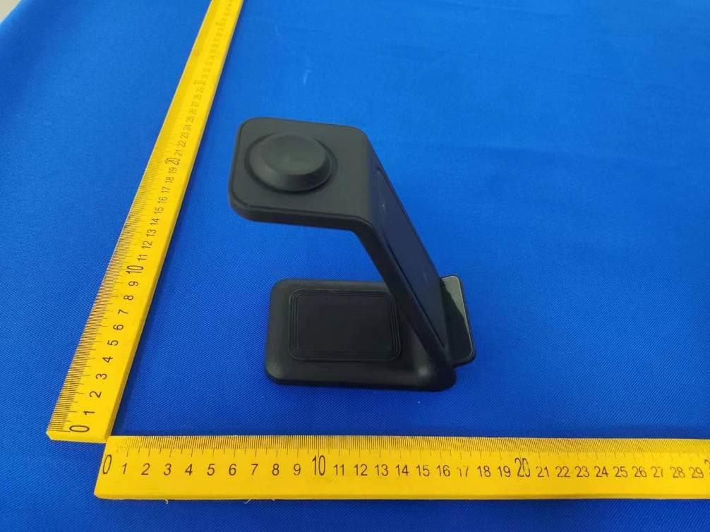
2AND8-CHG3N1
Aug 07, 20233-In-1 Fast Wireless Charging Station
Equipment Class
DCD - Part 15 Low Power Transmitter Below 1705 kHz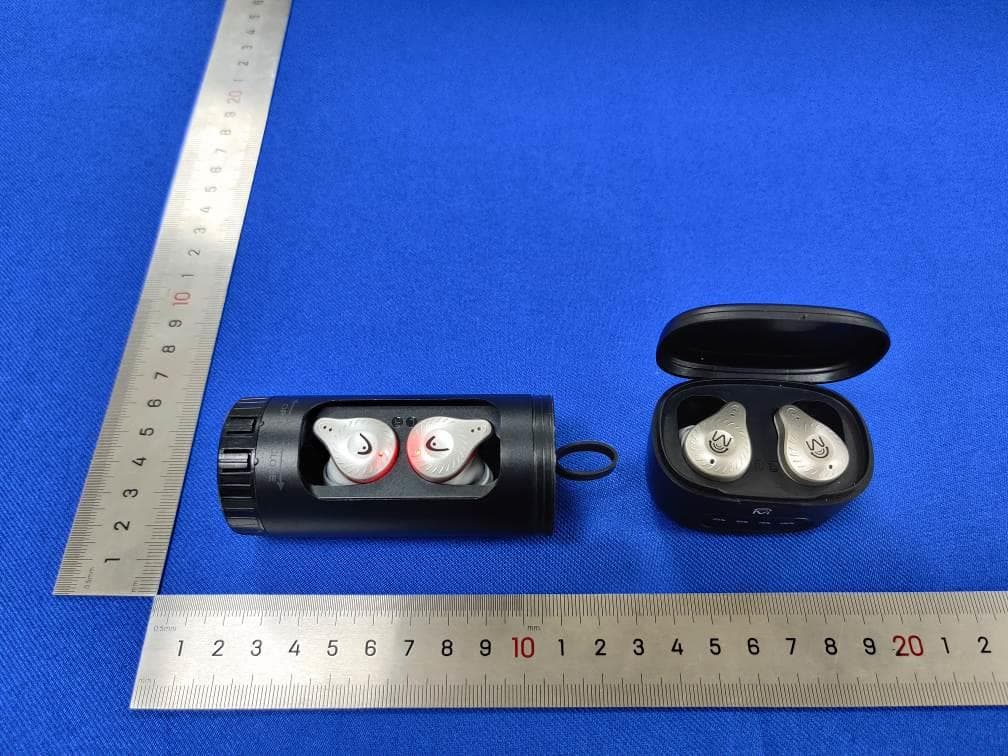
2AND8-TWS2304
May 22, 2023TWS EARBUDS
Equipment Class
DSS - Part 15 Spread Spectrum Transmitter2AND8-CH2207
Jul 25, 20224-in-1 Fast Wireless Charging Station With Lamp
Equipment Class
DCD - Part 15 Low Power Transmitter Below 1705 kHz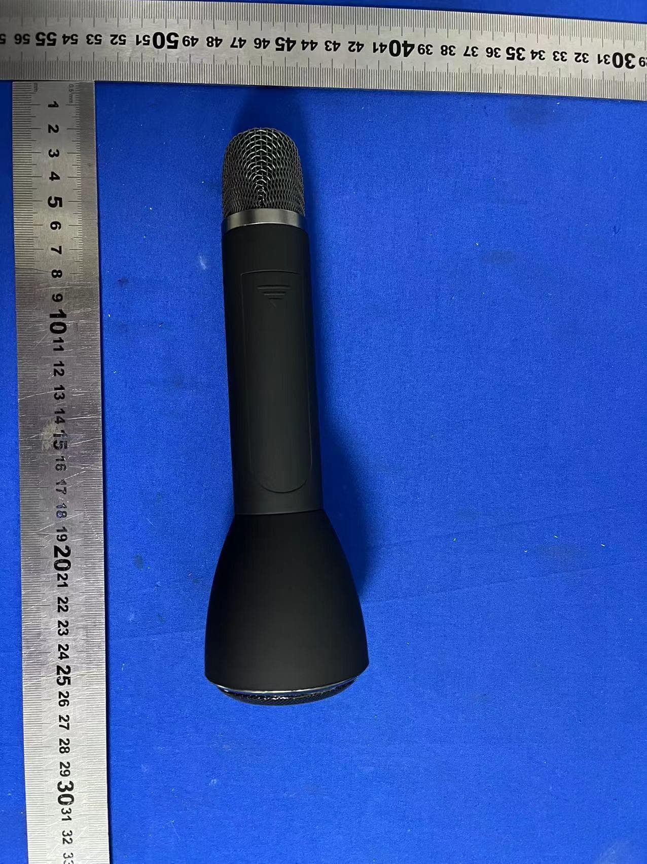
2AND8-BT2205
Jul 19, 2022Karaoke Wireless Microphone
Equipment Class
DSS - Part 15 Spread Spectrum Transmitter