2ANPO00NRF9161IOT Module
Nordic Semiconductor ASA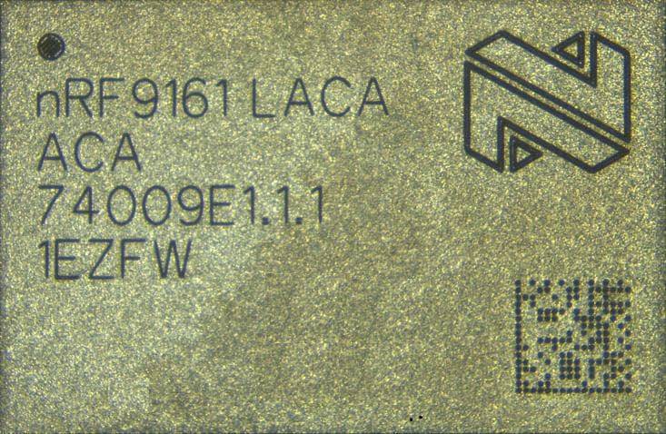
Click to zoom
Application Details
- Equipment Class
- PCB - PCS Licensed Transmitter
- Date of Grant
- Dec 19, 2023
- Application Purpose
- Original Equipment
- Date of Application
- Nov 29, 2023
- Equipment Note
- IOT Module
- Frequency Range
- 824.00000000 - 824.00000000
- Company
- Nordic Semiconductor ASA
- Country
- Norway
Documents & Files
Document Text
Text extracted from the exhibit documents filed with the FCC. Open a document above to read the original.
Users Manual
nRF9161 Objective Product Specification v0.7 4510_014 v0.7 / 2023-05-15 nRF9161 features Features: Microcontroller: •Arm ® Cortex ® -M33 •247 EEMBC CoreMark score running from flash memory •Data watchpoint and trace (DWT), embedded trace macrocell (ETM), and instrumentation trace macrocell (ITM) •Serial wire debug (SWD) •Trace port •1 MB flash •256 kB low leakage RAM •Arm TrustZone ® •Arm CryptoCell ™ 310 •Up to 4x SPI master/slave with EasyDMA •Up to 4x I2C compatible two-wire master/slave with EasyDMA •Up to 4x UART (CTS/RTS) with EasyDMA •I2S with EasyDMA •Digital microphone interface (PDM) with EasyDMA •4x pulse width modulator (PWM) unit with EasyDMA •12-bit, 200 ksps ADC with EasyDMA - eight configurable channels with programmable gain •3x 32-bit timer with counter mode •2x real-time counter (RTC) •Programmable peripheral interconnect (PPI) •32 general purpose I/O pins •Single supply voltage: 3.0 – 5.5 V •All necessary clock sources integrated •Package: 10 × 16 x 1.04 mm LGA LTE modem: •Transceiver and baseband •3GPP LTE release 14 Cat-M1 compliant •3GPP LTE release 14 Cat-NB1 and Cat-NB2 compliant •GPS receiver •GPS L1 C/A supported •QZSS L1 C/A supported •RF transceiver for global coverage •Up to 23 dBm output power •-108 dBm sensitivity (Cat-M1) for low band, -107 dBm for mid band •Single 50 Ω antenna interface •LTE band support in hardware: •Cat-M1: B1, B2, B3, B4, B5, B8, B12, B13, B18, B19, B20, B25, B26, B28, B66, B85 •Cat-NB1/NB2: B1, B2, B3, B4, B5, B8, B12, B13, B17, B19, B20, B25, B26, B28, B65, B66, B85 •Supports SIM and eSIM with an ETSI TS 102 221 compatible UICC interface •Power saving features: DRX, eDRX, PSM •IP v4/v6 stack •Secure socket (TLS/DTLS) API DECT NR+: •NR+ band: 1, 2, 9 Current consumption @ 3.7 V: •LTE power saving mode (PSM) floor current: 2.7 μA •eDRX @ 81.92s: 18 μA in Cat-M1, 32 μA in Cat-NB1 (UICC included) Applications: •Sensor networks •Logistics and asset tracking •Smart energy •Smart building automation •Smart agriculture •Industrial •Retail and monitor devices •Medical devices •Wearables 4510_014 v0.7 ii Contents nRF9161 features . . . . . . . . . . . . . . . . . . . . . . . . . . . . . . . . . .ii 1Revision history. . . . . . . . . . . . . . . . . . . . . . . . . . . . . . . .10 2About this document. . . . . . . . . . . . . . . . . . . . . . . . . . . . .11 2.1 Document status. . . . . . . . . . . . . . . . . . . . . . . . . . . . . . . .11 2.2 Peripheral chapters. . . . . . . . . . . . . . . . . . . . . . . . . . . . . . .11 2.2.2 Peripheral instantiation. . . . . . . . . . . . . . . . . . . . . . . . . . . .11 2.3 Register tables. . . . . . . . . . . . . . . . . . . . . . . . . . . . . . . . .12 2.3.1 Fields and values. . . . . . . . . . . . . . . . . . . . . . . . . . . . . . .12 2.3.2 Permissions. . . . . . . . . . . . . . . . . . . . . . . . . . . . . . . . .13 2.4 Registers. . . . . . . . . . . . . . . . . . . . . . . . . . . . . . . . . . . .13 2.4.1 DUMMY. . . . . . . . . . . . . . . . . . . . . . . . . . . . . . . . . .13 3Product overview. . . . . . . . . . . . . . . . . . . . . . . . . . . . . . .14 3.1 Block diagram. . . . . . . . . . . . . . . . . . . . . . . . . . . . . . . . . .14 3.2 Peripheral interface. . . . . . . . . . . . . . . . . . . . . . . . . . . . . . .15 3.2.1 Peripheral ID. . . . . . . . . . . . . . . . . . . . . . . . . . . . . . . .16 3.2.2 Peripherals with shared ID. . . . . . . . . . . . . . . . . . . . . . . . . . .17 3.2.3 Peripheral registers. . . . . . . . . . . . . . . . . . . . . . . . . . . . . .17 3.2.4 Bit set and clear. . . . . . . . . . . . . . . . . . . . . . . . . . . . . . .17 3.2.5 Tasks. . . . . . . . . . . . . . . . . . . . . . . . . . . . . . . . . . . .18 3.2.6 Events. . . . . . . . . . . . . . . . . . . . . . . . . . . . . . . . . . .18 3.2.7 Publish and subscribe. . . . . . . . . . . . . . . . . . . . . . . . . . . . .18 3.2.8 Shortcuts. . . . . . . . . . . . . . . . . . . . . . . . . . . . . . . . . .18 3.2.9 Interrupts. . . . . . . . . . . . . . . . . . . . . . . . . . . . . . . . . .18 3.2.10 Secure/non-secure peripherals. . . . . . . . . . . . . . . . . . . . . . . .19 4Application core . . . . . . . . . . . . . . . . . . . . . . . . . . . . . . . .20 4.1 CPU. . . . . . . . . . . . . . . . . . . . . . . . . . . . . . . . . . . . . .20 4.1.1 Floating-point interrupt. . . . . . . . . . . . . . . . . . . . . . . . . . . .20 4.1.2 CPU and support module configuration. . . . . . . . . . . . . . . . . . . . .20 4.1.3 Electrical specification. . . . . . . . . . . . . . . . . . . . . . . . . . . .21 4.2 Memory. . . . . . . . . . . . . . . . . . . . . . . . . . . . . . . . . . . .21 4.2.1 Memory map. . . . . . . . . . . . . . . . . . . . . . . . . . . . . . . .23 4.2.2 Instantiation. . . . . . . . . . . . . . . . . . . . . . . . . . . . . . . . .25 4.2.3 Peripheral access control capabilities. . . . . . . . . . . . . . . . . . . . . .27 4.3 VMC — Volatile memory controller. . . . . . . . . . . . . . . . . . . . . . . . .28 4.3.1 Registers. . . . . . . . . . . . . . . . . . . . . . . . . . . . . . . . . .28 4.4 NVMC — Non-volatile memory controller. . . . . . . . . . . . . . . . . . . . . .29 4.4.1 Writing to flash. . . . . . . . . . . . . . . . . . . . . . . . . . . . . . .29 4.4.2 Erasing a secure page in flash. . . . . . . . . . . . . . . . . . . . . . . . .30 4.4.3 Erasing a non-secure page in flash. . . . . . . . . . . . . . . . . . . . . . .30 4.4.4 Writing to user information configuration registers (UICR). . . . . . . . . . . . . .30 4.4.5 Erase all . . . . . . . . . . . . . . . . . . . . . . . . . . . . . . . . . .30 4.4.6 NVMC protection mechanisms. . . . . . . . . . . . . . . . . . . . . . . . .31 4.4.7 Cache. . . . . . . . . . . . . . . . . . . . . . . . . . . . . . . . . . .31 4.4.8 Registers. . . . . . . . . . . . . . . . . . . . . . . . . . . . . . . . . .32 4.4.9 Electrical specification. . . . . . . . . . . . . . . . . . . . . . . . . . . .35 4510_014 v0.7 iii 4.5 FICR — Factor…
Text truncated - open the document above for the full version.
Users Manual
Peripherals Bit number313029282726252423222120191817161514131211109876543210 IDBAAAAAAAA Reset 0x0000000000000000000000000000000000000000 IDR/WFieldValue IDValueDescription ARWCHIDX[0..255]DPPI channel that task SEQSTART[n] will subscribe to BRWEN Disabled0Disable subscription Enabled1Enable subscription 6.10.5.6 SUBSCRIBE_NEXTSTEP Address offset: 0x090 Subscribe configuration for task NEXTSTEP Bit number313029282726252423222120191817161514131211109876543210 IDBAAAAAAAA Reset 0x0000000000000000000000000000000000000000 IDR/WFieldValue IDValueDescription ARWCHIDX[0..255]DPPI channel that task NEXTSTEP will subscribe to BRWEN Disabled0Disable subscription Enabled1Enable subscription 6.10.5.7 EVENTS_STOPPED Address offset: 0x104 Response to STOP task, emitted when PWM pulses are no longer generated Bit number313029282726252423222120191817161514131211109876543210 IDA Reset 0x0000000000000000000000000000000000000000 IDR/WFieldValue IDValueDescription ARWEVENTS_STOPPEDResponse to STOP task, emitted when PWM pulses are no longer generated NotGenerated0Event not generated Generated1Event generated 6.10.5.8 EVENTS_SEQSTARTED[n] (n=0..1) Address offset: 0x108 + (n × 0x4) First PWM period started on sequence n Bit number313029282726252423222120191817161514131211109876543210 IDA Reset 0x0000000000000000000000000000000000000000 IDR/WFieldValue IDValueDescription ARWEVENTS_SEQSTARTEDFirst PWM period started on sequence n NotGenerated0Event not generated Generated1Event generated 6.10.5.9 EVENTS_SEQEND[n] (n=0..1) Address offset: 0x110 + (n × 0x4) 4510_014 v0.7 176 Peripherals Emitted at end of every sequence n, when last value from RAM has been applied to wave counter Bit number313029282726252423222120191817161514131211109876543210 IDA Reset 0x0000000000000000000000000000000000000000 IDR/WFieldValue IDValueDescription ARWEVENTS_SEQENDEmitted at end of every sequence n, when last value from RAM has been applied to wave counter NotGenerated0Event not generated Generated1Event generated 6.10.5.10 EVENTS_PWMPERIODEND Address offset: 0x118 Emitted at the end of each PWM period Bit number313029282726252423222120191817161514131211109876543210 IDA Reset 0x0000000000000000000000000000000000000000 IDR/WFieldValue IDValueDescription ARWEVENTS_PWMPERIODENDEmitted at the end of each PWM period NotGenerated0Event not generated Generated1Event generated 6.10.5.11 EVENTS_LOOPSDONE Address offset: 0x11C Concatenated sequences have been played the amount of times defined in LOOP.CNT This event triggers after the last SEQ[1] completion of the loop, and only if looping was enabled (LOOP > 0) when the sequence playback was started. Bit number313029282726252423222120191817161514131211109876543210 IDA Reset 0x0000000000000000000000000000000000000000 IDR/WFieldValue IDValueDescription ARWEVENTS_LOOPSDONEConcatenated sequences have been played the amount of times defined in LOOP.CNT This event triggers after the last SEQ[1] completion of the loop, and only if looping was enabled (LOOP > 0) when the sequence playback was started. NotGenerated0Event not generated Generated1Event generated 6.10.5.12 PUBLISH_STOPPED Address offset: 0x184 Publish configuration for event STOPPED 4510_014 v0.7 177 Peripherals Bit number313029282726252423222120191817161514131211109876543210 IDBAAAAAAAA Reset 0x0000000000000000000000000000000000000000 IDR/WFieldValue IDValueDescription ARWCHIDX[0..255]DPPI channel that event STOPPED will publish to BRWEN Disabled0Disable publishing Enabled1Enable publishing 6.10.5.13 PUBLISH_SEQSTARTED[n] (n=0..1) Address offset: 0x188 + (n × 0x4) Publish configuration for event SEQSTARTED[n] Bit number313029282726252423222120191817161514131211109876543210 IDBAAAAAAAA Reset 0x0000000000000000000000000000000000000000 IDR/WFieldValue IDValueDescription ARWCHIDX[0..255]DPPI channel that event SEQSTARTED[n] will publish to BRWEN Disabled0Disable publishing Enabled1Enable publishing 6.10.5.14 PUBLISH_SEQEND[n] (n=0..1) Address offset: 0x190 + (n × 0x4) Publish configuration for event SEQEND[n] Bit number313029282726252423222120191817161514131211109876543210 IDBAAAAAAAA Reset 0x0000000000000000000000000000000000000000 IDR/WFieldValue IDValueDescription ARWCHIDX[0..255]DPPI channel that event SEQEND[n] will publish to BRWEN Disabled0Disable publishing Enabled1Enable publishing 6.10.5.15 PUBLISH_PWMPERIODEND Address offset: 0x198 Publish configuration for event PWMPERIODEND Bit number313029282726252423222120191817161514131211109876543210 IDBAAAAAAAA Reset 0x0000000000000000000000000000000000000000 IDR/WFieldValue IDValueDescription ARWCHIDX[0..255]DPPI channel that event PWMPERIODEND will publish to BRWEN Disabled0Disable publishing Enabled1Enable publishing 4510_014 v0.7 178 Peripherals 6.10.5.16 PUBLISH_LOOPSDONE Address offset: 0x19C Publish configuration for event LOOPSDONE This event triggers after the last SEQ[1] completion of the loop, and only if looping was enabled (LOOP > 0) when the sequence playback was started. Bit number313029282726252423222120191817161514131211109876543210 IDBAAAAAAAA Reset 0x0000000000000000000000000000000000000000 IDR/WFieldValue IDValueDescription ARWCHIDX[0..255]DPPI channel that event LOOPSDONE will publish to BRWEN Disabled0Disable publishing Enabled1Enable publishing 6.10.5.17 SHORTS Address offset: 0x200 Shortcuts between local events and tasks Bit number313029282726252423222120191817161514131211109876543210 IDEDCBA Reset 0x0000000000000000000000000000000000000000 IDR/WFieldValue IDValueDescription ARWSEQEND0_STOPShortcut between event SEQEND[0] and task STOP Disabled0Disable shortcut Enabled1Enable shortcut BRWSEQEND1_STOPShortcut between event SEQEND[1] and task STOP Disabled0Disable shortcut Enabled1Enable shortcut CRWLOOPSDONE_SEQSTART0Shortcut between event LOOPSDONE and task SEQSTART[0] Disabled0Disable shortcut Enabled1Enable shortcut DRWLOOPSDONE_SEQSTART1Shortcut between event LOOPSDONE and task SEQSTART[1] Disabled0Disable shortcut Enabled1Enable shortcut ERWLOOPSDONE_STOPShort…
Text truncated - open the document above for the full version.
Users Manual
Peripherals Bit number313029282726252423222120191817161514131211109876543210 IDAAAAAAAAAAAAAAAAAAAAAAAAAAAAAAAA Reset 0x0400000000000100000000000000000000000000 IDR/WFieldValue IDValueDescription Baud192000x004EA00019200 baud (actual rate: 19208) Baud288000x0075C00028800 baud (actual rate: 28777) Baud312500x0080000031250 baud Baud384000x009D000038400 baud (actual rate: 38369) Baud560000x00E5000056000 baud (actual rate: 55944) Baud576000x00EB000057600 baud (actual rate: 57554) Baud768000x013A900076800 baud (actual rate: 76923) Baud1152000x01D60000115200 baud (actual rate: 115108) Baud2304000x03B00000230400 baud (actual rate: 231884) Baud2500000x04000000250000 baud Baud4608000x07400000460800 baud (actual rate: 457143) Baud9216000x0F000000921600 baud (actual rate: 941176) Baud1M0x100000001 megabaud 6.19.9.44 RXD RXD EasyDMA channel 6.19.9.44.1 RXD.PTR Address offset: 0x534 Data pointer Bit number313029282726252423222120191817161514131211109876543210 IDAAAAAAAAAAAAAAAAAAAAAAAAAAAAAAAA Reset 0x0000000000000000000000000000000000000000 IDR/WFieldValue IDValueDescription ARWPTRData pointer See the memory chapter for details about which memories are available for EasyDMA. 6.19.9.44.2 RXD.MAXCNT Address offset: 0x538 Maximum number of bytes in receive buffer Bit number313029282726252423222120191817161514131211109876543210 IDAAAAAAAAAAAAA Reset 0x0000000000000000000000000000000000000000 IDR/WFieldValue IDValueDescription ARWMAXCNT[1..0x1FFF]Maximum number of bytes in receive buffer 6.19.9.44.3 RXD.AMOUNT Address offset: 0x53C Number of bytes transferred in the last transaction 4510_014 v0.7 349 Peripherals Bit number313029282726252423222120191817161514131211109876543210 IDAAAAAAAAAAAAA Reset 0x0000000000000000000000000000000000000000 IDR/WFieldValue IDValueDescription ARAMOUNT[1..0x1FFF]Number of bytes transferred in the last transaction 6.19.9.45 TXD TXD EasyDMA channel 6.19.9.45.1 TXD.PTR Address offset: 0x544 Data pointer Bit number313029282726252423222120191817161514131211109876543210 IDAAAAAAAAAAAAAAAAAAAAAAAAAAAAAAAA Reset 0x0000000000000000000000000000000000000000 IDR/WFieldValue IDValueDescription ARWPTRData pointer See the memory chapter for details about which memories are available for EasyDMA. 6.19.9.45.2 TXD.MAXCNT Address offset: 0x548 Maximum number of bytes in transmit buffer Bit number313029282726252423222120191817161514131211109876543210 IDAAAAAAAAAAAAA Reset 0x0000000000000000000000000000000000000000 IDR/WFieldValue IDValueDescription ARWMAXCNT[1..0x1FFF]Maximum number of bytes in transmit buffer 6.19.9.45.3 TXD.AMOUNT Address offset: 0x54C Number of bytes transferred in the last transaction Bit number313029282726252423222120191817161514131211109876543210 IDAAAAAAAAAAAAA Reset 0x0000000000000000000000000000000000000000 IDR/WFieldValue IDValueDescription ARAMOUNT[1..0x1FFF]Number of bytes transferred in the last transaction 6.19.9.46 CONFIG Address offset: 0x56C Configuration of parity and hardware flow control 4510_014 v0.7 350 Peripherals Bit number313029282726252423222120191817161514131211109876543210 IDCBBB Reset 0x0000000000000000000000000000000000000000 IDR/WFieldValue IDValueDescription RWHWFCHardware flow control Disabled0Disabled Enabled1Enabled BRWPARITYParity Excluded0x0Exclude parity bit Included0x7Include even parity bit CRWSTOPStop bits One0One stop bit Two1Two stop bits 6.19.10 Electrical specification 6.19.10.1 UARTE electrical specification SymbolDescriptionMin.Typ.Max.Units f UARTE Baud rate for UARTE 22 . 1000kbps t UARTE,CTSH CTS high time1μs t UARTE,START Time from STARTRX/STARTTX task to transmission started0.25μs 6.20 WDT — Watchdog timer A countdown watchdog timer using the low-frequency clock source (LFCLK) offers configurable and robust protection against application lock-up. The watchdog timer is started by triggering the START task. The watchdog can be paused during long CPU sleep periods for low power applications and when the debugger has halted the CPU. The watchdog is implemented as a down-counter that generates a TIMEOUT event when it wraps over after counting down to 0. When the watchdog timer is started through the START task, the watchdog counter is loaded with the value specified in the CRV register. This counter is also reloaded with the value specified in the CRV register when a reload request is granted. The watchdog’s timeout period is given by: timeout [s] = ( CRV + 1 ) / 32768 When started, the watchdog will automatically force the 32.768 kHz RC oscillator on as long as no other 32.768 kHz clock source is running and generating the 32.768 kHz system clock, see chapter CLOCK — Clock control on page 70. 6.20.1 Reload criteria The watchdog has eight separate reload request registers, which shall be used to request the watchdog to reload its counter with the value specified in the CRV register. To reload the watchdog counter, the special value 0x6E524635 needs to be written to all enabled reload registers. One or more RR registers can be individually enabled through the RREN register. 22 High baud rates may require GPIOs to be set as High Drive, see GPIO chapter for more details. 4510_014 v0.7 351 Peripherals 6.20.2 Temporarily pausing the watchdog By default, the watchdog will be active counting down the down-counter while the CPU is sleeping and when it is halted by the debugger. It is however possible to configure the watchdog to automatically pause while the CPU is sleeping as well as when it is halted by the debugger. 6.20.3 Watchdog reset A TIMEOUT event will automatically lead to a watchdog reset. See Reset on page 56 for more information about reset sources. If the watchdog is configured to generate an interrupt on the TIMEOUT event, the watchdog reset will be postponed with two 32.768 kHz clock cycles after the TIMEOUT event has been generated. Once the TIMEOUT event has been generated, the impending watchdog reset will always be effectuated. The watchdog must be configured before it is started. After it is started, the watchdog’s co…
Text truncated - open the document above for the full version.
Attestation Statements
Date: 18.08.2023 DEKRA Testing and Certification, S.A.U. Parque Tecnológico de Andalucía C/ Severo Ochoa 2 & 6 29590 Campanillas Málaga, España Certifications concerning “covered” equipment. Section 2.911(d)(5)(i)- (ii) FCC ID: 2ANPO00nRF9161 We, Nordic Semiconductor ASA, located in Otto Nielsens veg 12, Trondheim, Norway; certify that: - the equipment for which authorization is sought is not “covered” equipment prohibited from receiving an equipment authorization pursuant to section 2.903 of the FCC rules. - as of the date of the filing of the application, the applicant is identified on the Covered List as an entity producing “covered” equipment. Sincerely, __________________________ By: Niko Balabanis Title: Certification Manager Company: Nordic Semiconductor ASA Telephone: +47 72898900 e-mail: [email protected]
Attestation Statements
Federal Communications Commission Authorization and Evaluation Division 7435 Oakland Mills Road Columbia, MD 21046 USA Date: 03-24-2023 Headquarters Otto Nielsens v 12, 7052 Trondheim, Norway Postal address: P.O. Box 2336, 7004 Trondheim Tel.: +47 72 89 89 00 www.nordicsemi.com NO 966 011 726 MVA Page 1 of 1 Ref: Attestation Statements Part 2.911(d)(7) Filing FCC ID: 2ANPO00NRF9160 NORDIC SEMICONDUCTOR ASA (“the applicant”) certifies that, as of the date of the filing of the application, TianHeng Consulting, LLC is our designated U.S. agent for service of process for the above referenced FCC ID. NORDIC SEMICONDUCTOR ASA accepts to maintain an agent for no less than one year after the grantee has terminated all marketing and importation or the conclusion of any Commission- related proceeding involving the equipment. TianHeng Consulting, LLC accepts, as of the date of the filing of the application, the obligation of the designated U.S. agent for service of process for the above referenced FCC ID. Sincerely, Designated U.S. Agent Information: Name: TianHeng Consulting, LLC FRN: 0033401258 Contact Person: Hualing Dong Address: 392 Andover Street, Wilmington, MA 01887, United States Tel.: +1 617-997-4010 Email: [email protected] U.S. Agent Signature: Applicant: Company Name: NORDIC SEMICONDUCTOR ASA Grantee Code: 2ANPO Applicant FRN: 0026827089 Contact Name: Ketil Aas-Johansen Address:Otto Nielsens vei 12, 7052 Trondheim, Norway Tel.: +47 72898900 Email: [email protected] Applicant Signature: Hualing Dong, President
Cover Letter(s)
Supported bands Date: 30/08/2023 Federal Communications Commission Equipment Authorization Branch 7435 Oakland Mills Rd. Columbia MD 21046 FCC ID: 2ANPO00nRF9161 To whom it may concern: We, Nordic Semiconductor ASA, Otto Nielsens veg 12, 7052 Trondheim, Norway . hereby declare that Product object of this approval process operates only in the LTE Cat M1 bands 2, 4, 5, 8, 12, 13, 25, 26, 66, 71, 85; and NB-IoT bands 2, 4, 5, 8, 12, 13, 17, 25, 26, 66, 71, 85 in the US, and the other supported bands will be disabled by SW. Sincerely, By: Niko Balabanis Title: Certification Manager Telephone: +47 72898900 e-mail: [email protected]
Cover Letter(s)
Date: 18.08.2023 DEKRA Testing and Certification, S.A.U. Parque Tecnológico de Andalucía C/ Severo Ochoa 2 & 6 29590 Campanillas Málaga, España Ref: Agent letter for FCC ID: 2ANPO00nRF9161 We, Nordic Semiconductor ASA, Otto Nielsens veg 12, 7052 Trondheim, Norway hereby authorize DEKRA Testing and Certification, S.A.U , Severo Ochoa, 2 & 6, 29590 Malaga, Spain Ms. María Rodríguez Moyano, e-mail: [email protected], Phone: +34 952 619 114 to act as our agent in the preparation of this application for equipment certification, including the signing of all documents relating to these matters. The present authorization considers the development of documents on behalf of the client, written under his own letterhead and related to the necessary information to be provided on his behalf to complete the certification process. We also hereby certify that neither we nor any party to this application are subject to a denial of U.S. Federal benefits, which include FCC benefits, pursuant to Section 5301 of the Anti-Drug Abuse Act of 1988, U.S.C. 862 because of conviction for possession or distribution of controlled substance. For instances where our authorized agent signs the application for certification on our behalf, I acknowledge that all responsibility for complying with the terms and conditions for Certification, as specified by DEKRA Testing and Certification, S.A.U. , still resides with us. This agreement expires one year from the current date. Sincerely, __________________________ By: Niko Balabanis Title: Certification Manager Company: Nordic Semiconductor ASA Telephone: +47 72898900 e-mail: [email protected]
Cover Letter(s)
Date: 21 November 2023 B71 removal letter Manufacturer: Nordic Semiconductor ASA Model: nRF9161 FCC ID: 2ANPO00NRF9161 PMN: nRF9161 HVIN: nRF9161 IC: 24529-NRF9161 HMN: N/A FVIN: mfw_nrf91x1_2.0.0 We, Nordic Semiconductor ASA declares that our module Nordic nRF9161 does not support B71 connectivity for LTE Cat-M1 and NB-IoT technologies. In the beginning, this band was supported and duly tested. However, we have decided to remove B71 due to limited carrier s upport for this band. Yours sincerely, ______________________________________ By: Niko Balabanis Title: Certification Manager Company: Nordic semiconductor ASA Telephone: +47 72898900 e- mail: [email protected]
Cover Letter(s)
Date: 18.08.2023 DEKRA Testing and Certification, S.A.U. Parque Tecnológico de Andalucía C/ Severo Ochoa 2 & 6 29590 Campanillas Málaga, España Ref: Confidentiality request for FCC ID: 2ANPO00nRF9161 To whom it may concern: Pursuant to §0.457(d)(1)(ii) and §0.459 of the Commission’s Rules (47 C.F.R.) and §552 (b)(4) of the Freedom of Information Act, Nordic Semiconductor ASA hereby request requests that a part of the subject FCC application be held confidential to avoid release of sensitive information of the product to the public. For the product stated above, we request that the following information be withheld from public disclose: Type of Confidentiality Requested Exhibit Short Term Permanent Block Diagrams Short Term External Photos Short Term Internal Photos Short Term Permanent Operation Description Short Term Permanent Parts List & Placement/BOM Short Term Permanent Tune-Up Procedure Short Term Permanent Schematics Short Term Test Setup Photos Short Term User’s Manual Short Term Permanent SDR software and security information Permanent Confidentiality: The above materials contain trade secrets and proprietary information not customarily released to the public. The public disclosure of these matters might be harmful to us and provide unjustified benefits to our competitors. Short-Term Confidentiality: We hereby request short-term confidentiality for the product stated above to avoid premature release of sensitive information prior to marketing or release of the product to the public. Release date of short term confidentiality is: 45 days from grant date marked 90 days from grant date marked 135 days from grant date marked 180 days from grant date marked Specific date: We are also aware that we are responsible to notify DEKRA in the event information regarding the product or the product is made available to the public. DEKRA will then release the documents listed above for public disclosure pursuant to FCC Public Notice DA 04-1705. Sincerely, __________________________ By: Niko Balabanis Title: Certification Manager Company: Nordic Semiconductor ASA Telephone: +47 72898900 e-mail: [email protected]
Cover Letter(s)
FCB013_02 //DEKRA Testing and Certification, S.A.U. // www.dekra-product-safety.com/wireless Date: 30/11/2023 DEKRA Testing and Certification, S.A.U. Parque Tecnológico de Andalucía C/ Severo Ochoa 2 & 6 29590 Campanillas Málaga, España Ref: FCC Modular approval letter for FCC ID: 2ANPO00NRF9161 To whom it may concern: The following attestation addresses the requirements to support modular approval pursuant to §15.212 of the Commission’s Rules: Modular approval requirement Yes No* (i) The radio elements of the modular transmitter must have their own shielding. The physical crystal and tuning capacitors may be located external to the shielded radio elements. X (ii) The modular transmitter must have buffered modulation/data inputs (if such inputs are provided) to ensure that the module will comply with part 15 requirements under conditions of excessive data rates or over-modulation. X (iii) The modular transmitter must have its own power supply regulation. X (iv) The modular transmitter must comply with the antenna and transmission system requirements of §§15.203, 15.204(b) and 15.204(c). The antenna must either be permanently attached or employ a “unique” antenna coupler (at all connections between the module and the antenna, including the cable). The “professional installation” provision of §15.203 is not applicable to modules but can apply to limited modular approvals under paragraph (b) of this section. X (v) The modular transmitter must be tested in a stand-alone configuration, i.e., the module must not be inside another device during testing for compliance with part 15 requirements. Unless the transmitter module will be battery powered, it must comply with the AC line conducted requirements found in §15.207. AC or DC power lines and data input/output lines connected to the module must not contain ferrites, unless they will be marketed with the module (see §15.27(a)). The length of these lines shall be the length typical of actual use or, if that length is unknown, at least 10 centimeters to insure that there is no coupling between the case of the module and supporting equipment. Any accessories, peripherals, or support equipment connected to the module during testing shall be unmodified and commercially available (see §15.31(i)). X (vi) The modular transmitter must be equipped with either a permanently affixed label or must be capable of electronically displaying its FCC identification number. X (vii) The modular transmitter must comply with any specific rules or operating requirements that ordinarily apply to a complete transmitter and the manufacturer must provide adequate instructions along with the module to explain any such requirements. A copy of these instructions must be included in the application for equipment authorization. X (viii) The modular transmitter must comply with any applicable RF exposure requirements in its final configuration. X * Shall provide a detailed explanation if the answer is “No”. Sincerely, __________________________ By: Niko Balabanis Title: Certification Manager Company: Nordic Semiconductor ASA Telephone: +47 72898900 e-mail: [email protected]
Cover Letter(s)
Date: 27 November 2023 NB-IoT offset description Manufacturer: Nordic Semiconductor ASA Model: nRF9161 FCC ID: 2ANPO00NRF9161 We, Nordic Semiconductor ASA, hereby states that our module nRF9161 has been tested to certify Cat M1 and NB-IoT bands for FCC and ISED certification. The strategy followed to perform this testing was finding the channels outermost of the bands, which complies with the block edge testing; accordingly, we can demonstrate the lowest and highest channels for NB-IoT bands are the following ones: Channel Number (Frequency MHz) – NB-IoT B2 B4 B5 B8 B12 B13 B17 B25 B26 B66 B85 Lowest 18602 (1850.2) 19952 (1710.2) 20402 (824.20) 21628 (897.80) 23012 (699.20) 23182 (777.20) 23732 (704.20) 26042 (1850.2) 20402 (814.20) 131974 (1710.2) 134004 (698.2) Middle 18900 (1880) 20300 (1745) 20525 (836.50) 21640 (899) 23090 (707) 23230 (782) 23790 (710) 26365 (1882.5) 20525 (836.50) 132322 (1745) 134092 (707) Highest 19198 (1909.8) 132670 (1754.8) 20648 (848.80) 21652 (900.20) 23179 (715.9) 23278 (786.80) 23848 (715.80) 26688 (1914.8) 20648 (848.80) 132670 (1779.8) 134181 (715.9) For NB-IoT technology, an offset of ± 100 kHz for the first/last transmission channel is needed because the bandwidth required for a transmission is 200 kHz. However, for some bands it has been adjusted the lower and/or…
Text truncated - open the document above for the full version.
Contact Information
Applicant
Niko Balabanis(Certification manager)
Test Firm
DEKRA Testing and Certification, S.A.U.Rafael Lopez Martin
Technical Specifications
| # | Rule Parts | Frequency Range | Power Output | Emission | Tolerance |
|---|---|---|---|---|---|
| 32 | 22H,9 | 824 MHz - 824 MHz | 180.00 mW | 186KG7W | 1 ppm |
Other Applications from Nordic Semiconductor ASA
2ANPO00NRF9151
Apr 04, 2024Wireless hearing instrument
Equipment Class
PCB - PCS Licensed Transmitter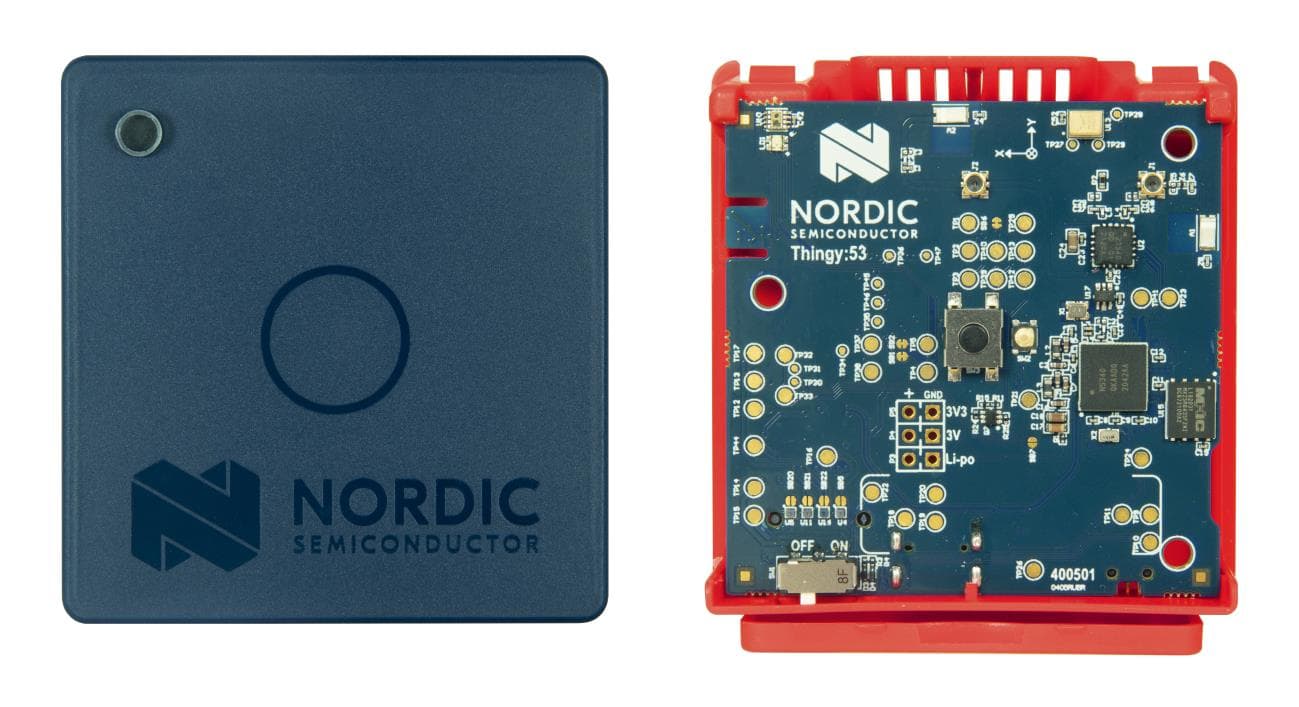
2ANPOTHINGY53
Jun 21, 2022Thingy 53
Equipment Class
JBP - Part 15 Class B Computing Device Peripheral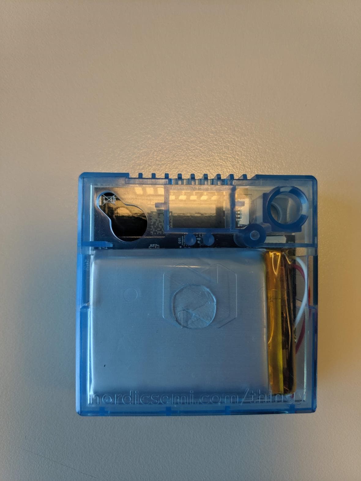
2ANPOTHINGY91
Jan 27, 2020Thingy 91
Equipment Class
JBP - Part 15 Class B Computing Device Peripheral