2AO4FM010-3Portable payment terminal
Miura Systems Ltd
Click to zoom
Application Details
- Equipment Class
- DSS - Part 15 Spread Spectrum Transmitter
- Date of Grant
- Jan 12, 2020
- Application Purpose
- Original Equipment
- Date of Application
- Jan 12, 2020
- Equipment Note
- Portable payment terminal
- Frequency Range
- 2402.00000000 - 2480.00000000
- Company
- Miura Systems Ltd
- Country
- United Kingdom
Documents & Files
Document Text
Text extracted from the exhibit documents filed with the FCC. Open a document above to read the original.
Users Manual
© Miura Systems 2019 Page 1 of 25 Registered office: Miura Systems Ltd, Unit 3, Cliveden Office Village, Lancaster Road, Cressex Industrial Estate, High Wycombe HP12 3YZ Company no: 06714257 Vat reg: 940 6618 21 M010-GUIDE01-V1-3 M010 Operational Guide Date: 3 rd June 2019 Commercially confidential Uncontrolled when printed Document History Version Details of change(s) Author(s) V1-0 Initial release RS, RH, VB V1-1 Added battery charging recommendations, and regulatory statements. MW, SJ V1-2 Added implementation note about Vehicle transients. Added new compliance notes, NFC. DH, RS V1-3 Storage battery recharge statement added, formatting changes, in vehicle use note added. ‘Shuttle’ references updated except in log files GR M010-GUIDE01-V1-3 Confidential © Miura Systems 2019 Page 2 of 25 Registered office: Miura Systems Ltd, Unit 3, Cliveden Office Village, Lancaster Road, Cressex Industrial Estate, High Wycombe HP12 3YZ Company no: 06714257 Vat reg: 940 6618 21 1 Introduction .................................................................................................................................. 4 2 M010 Features .............................................................................................................................. 5 3 Operating the M010 Terminal ...................................................................................................... 6 3.1 Introduction ........................................................................................................................... 6 3.2 Power and charging ............................................................................................................... 6 3.2.1 Turning the terminal ON ................................................................................................ 6 3.2.2 Turning the terminal OFF ............................................................................................... 6 3.2.3 Sleep ............................................................................................................................... 6 3.2.4 Charging the Battery ...................................................................................................... 6 3.2.5 Low Battery .................................................................................................................... 7 3.2.6 Battery usage guidelines ................................................................................................ 7 3.2.7 Implementation note: vehicle transients ...................................................................... 7 3.3 Bluetooth ............................................................................................................................... 8 3.3.1 Start up ........................................................................................................................... 8 3.3.2 Ready To Pair: ................................................................................................................. 8 3.3.3 Ready To Connect........................................................................................................... 8 3.3.4 Connected ...................................................................................................................... 8 3.4 Transaction Mode .................................................................................................................. 9 3.4.1 PIN Entry ......................................................................................................................... 9 3.4.2 PIN OK ............................................................................................................................. 9 3.4.3 PIN Incorrect .................................................................................................................. 9 3.4.4 Last Try ............................................................................................................................ 9 3.5 Contactless ............................................................................................................................ 9 3.5.1 Contactless transactions .............................................................................................. 10 3.6 Terminal Maintenance ........................................................................................................ 10 3.6.1 Security Check .............................................................................................................. 10 3.6.2 Software Update .......................................................................................................... 10 3.7 Error states .......................................................................................................................... 11 3.7.1 System Tampered ......................................................................................................... 11 3.7.2 Ready To Install ............................................................................................................. 11 4 Revive TM ...................................................................................................................................... 12 4.1 Power up as Normal ............................................................................................................ 12 M010-GUIDE01-V1-3 Confidential © Miura Systems 2019 Page 3 of 25 Registered office: Miura Systems Ltd, Unit 3, Cliveden Office Village, Lancaster Road, Cressex Industrial Estate, High Wycombe HP12 3YZ Company no: 06714257 Vat reg: 940 6618 21 4.2 System Restore .................................................................................................................... 12 4.3 Total Factory reset ............................................................................................................... 13 4.4 Terminal Diagnostics .............................................................................................…
Text truncated - open the document above for the full version.
Cover Letter(s)
Miura Systems Ltd Agent Authorization Company: Miura Systems Ltd Address: Unit 3, Cliveden Office Village, Lancaster Road, Cressex Industrial Estate, High Wycombe HP12 3YZ, United Kingdom Product Name: Portable payment terminal Model Number(s): M010 Product Description: Portable payment terminal We authorize MiCOM Labs Inc., 575 Boulder Court, Pleasanton, California 94566, USA, to act on our behalf on all matters concerning the certification of above named equipment. We declare that MiCOM Labs Inc. is allowed to forward all information related to the approval and certification of equipment to the regulatory agencies as required and to discuss any issues concerning the approval application. Any and all acts carried out by MiCOM Labs on our behalf shall have the same effect as acts of our own. Signature: Date: 2020-01-08 Name: Gareth Richards Title: Chief Technical Officer Company: Miura Systems Ltd
Cover Letter(s)
Miura Systems Ltd Office of Engineering Technology Federal Communications Commission 7435 Oakland Mills Road Columbia, MD 21046 USA Date: 2020/01/08 Subject; Request for Confidentiality FCC ID: 2AO4FM010-3 To Whom It May Concern, Pursuant to the provisions of the Commission’s rules Title 47 Sections §0.457 and §0.459, we are requesting the Commission to withhold the following attachment(s) as confidential documents from public disclosure indefinitely. These documents contain detailed system and equipment descriptions and are considered as proprietary information in operation of the equipment. The public disclosure of these documents might be harmful to our company and would give competitors an unfair advantage in the market. Schematic Diagram Block Diagram Parts List Operational Description Tune-up Procedure It is our understanding that all measurement test reports, FCC ID label format and correspondence during the certification review process cannot be granted as confidential documents and this information will be available for public review once the grant of equipment authorization is issued. Sincerely, Signature: Name: Gareth Richards Title: Chief Technical Officer
External Photos
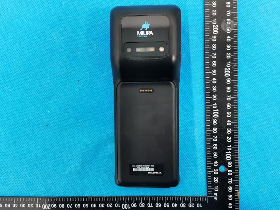
External photo HVIN: M010 HVIN: M010 HVIN: M010
ID Label/Location Info
Label Label Location HVIN: M010
Internal Photos
M/N: M010 Internal photo M/N: M010 M/N: M010 M/N: M010 Note: PCB board is multi-layer board and NFC antenna is integrated on PCB NFC Chip NFC Antenna M/N: M010 BT model BT Antenna
RF Exposure Info
Dongguan Nore Testing Center Co., Ltd. Report No.: NTC1910196EV00-1 IC: 23677-M0103 Page 1 of 3 RF EXPOSURE EVALUATION EUT Specification EUT Portable payment terminal Frequency band (Operating) 2.408GHz ~ 2.474GHz WLAN: 5.18GHz ~ 5.32GHz / 5.50GHz ~ 5.70GHz WLAN: 5.745GHz ~ 5.825GHz Others(Bluetooth: 2.402GHz ~ 2.480GHz) Others(NFC: 13.56MHz) Device category Portable (<20cm separation) Mobile (>20cm separation) Others ___ Antenna diversity Single antenna Multiple antennas Tx diversity Rx diversity Tx/Rx diversity Max. output power BT: 5.484dBm (3.966mW) NFC: -50.96 dBm (8.017e-6mW) Antenna gain 3.5 dBi for BT function 0 dBi for NFC function Evaluation applied MPE Evaluation SAR Evaluation Dongguan Nore Testing Center Co., Ltd. Report No.: NTC1910196EV00-1 IC: 23677-M0103 Page 2 of 3 Limits for RF Exposure Portable device – When the device operates at or below the applicable output power level (adjusted for tune-up tolerance) for the specified separation distance defined in below table. Output power level shall be the higher of the maximum conducted or equivalent isotropically radiated power (e.i.r.p.) source-based, time-averaged output power. For controlled use devices where the 8 W/kg for 1 gram of tissue applies, the exemption limits for routine evaluation in Table 1 are multiplied by a factor of 5. For limb-worn devices where the 10 gram value applies, the exemption limits for routine evaluation in Table 1 are multiplied by a factor of 2.5. If the operating frequency of the device is between two frequencies located in Table 1, linear interpolation shall be applied for the applicable separation distance. For test separation distance less than 5 mm, the exemption limits for a separation distance of 5 mm can be applied to determine if a routine evaluation is required. For medical implants devices, the exemption limit for routine evaluation is set at 1 mW. The output power of a medical implants device is defined as the higher of the conducted or e.i.r.p to determine whether the device is exempt from the SAR evaluation. Dongguan Nore Testing Center Co., Ltd. Report No.: NTC1910196EV00-1 IC: 23677-M0103 Page 3 of 3 Measurement Result At separation distance ≤5mm Channel Channel Frequency (MHz) Max Output power (dBm) Tolerance Max Output power (mW) Threshold Value (mW) Test Mode: GFSK Low 2402 4.124 ±0.5 2.900 4.0 Middle 2441 5.041 ±0.5 3.582 4.0 High 2480 5.484 ±0.5 3.966 4.0 Test Mode: π4/-DQPSK Low 2402 3.529 ±0.5 2.529 4.0 Middle 2441 4.545 ±0.5 3.195 4.0 High 2480 5.372 ±0.5 3.865 4.0 Test Mode: 8DPSK Low 2402 4.612 ±0.5 3.245 4.0 Middle 2441 5.288 ±0.5 3.791 4.0 High 2480 5.241 ±0.5 3.751 4.0 NFC Channel Channel Frequency (MHz) Max Output power (dBm) Max Output power (mW) - 13.56 -50.96 8.017e-6 EIRP= 44.30-104.8+20Log 3= -50.96 dBm According to RSS-102, separation distance is 5mm, and no SAR measurement is required.
Test Report
Dongguan Nore Testing Center Co., Ltd. Report No.: NTC1910194FV00 FCC ID: 2AO4FM010-3 Page 2 of 45 Table of Contents 1. GENERAL INFORMATION ................................................................................................ 5 1.1 PRODUCT DESCRIPTION FOR EQUIPMENT UNDER TEST ................................................................. 5 1.2 RELATED SUBMITTAL(S) / GRANT (S) ............................................................................................ 7 1.3 DEVIATIONS AND ABNORMALITIES FROM STANDARD CONDITIONS ................................................... 7 1.4 TEST METHODOLOGY .................................................................................................................. 7 1.5 EQUIPMENT MODIFICATIONS ........................................................................................................ 7 1.6 SUPPORT DEVICE ....................................................................................................................... 7 1.7 TEST FACILITY AND LOCATION ..................................................................................................... 8 1.8 SUMMARY OF TEST RESULTS ....................................................................................................... 9 2. SYSTEM TEST CONFIGURATION .................................................................................. 10 2.1 EUT CONFIGURATION ............................................................................................................... 10 2.2 SPECIAL ACCESSORIES ............................................................................................................. 10 2.3 DESCRIPTION OF TEST MODES ................................................................................................... 10 2.4 EUT EXERCISE ......................................................................................................................... 10 3. CONDUCTED EMISSIONS TEST .................................................................................... 11 3.1 TEST SET-UP (BLOCK DIAGRAM OF CONFIGURATION) ................................................................ 11 3.2 TEST CONDITION ....................................................................................................................... 11 3.3 MEASUREMENT RESULTS .......................................................................................................... 11 4. RADIATED EMISSION TEST ........................................................................................... 14 4.1 TEST SET-UP (BLOCK DIAGRAM OF CONFIGURATION) ................................................................ 14 4.2 MEASUREMENT PROCEDURE ..................................................................................................... 15 4.3 LIMIT ........................................................................................................................................ 16 4.4 MEASUREMENT RESULTS ................................................................................................. 16 5. CHANNEL SEPARATION TEST ...................................................................................... 20 5.1 MEASUREMENT PROCEDURE ..................................................................................................... 20 5.2 TEST SET-UP (BLOCK DIAGRAM OF CONFIGURATION) ................................................................ 20 5.3 MEASUREMENT RESULTS .......................................................................................................... 20 6. 20DB BANDWIDTH .......................................................................................................... 24 6.1 MEASUREMENT PROCEDURE ..................................................................................................... 24 6.2 TEST SET-UP (BLOCK DIAGRAM OF CONFIGURATION) ................................................................ 24 6.3 MEASUREMENT RESULTS .......................................................................................................... 24 7. HOPPING CHANNEL NUMBER ...................................................................................... 28 7.1 MEASUREMENT PROCEDURE ..................................................................................................... 28 7.2 TEST SET-UP (BLOCK DIAGRAM OF CONFIGURATION) ................................................................ 28 7.3 MEASUREMENT RESULTS .......................................................................................................... 28 Dongguan Nore Testing Center Co., Ltd. Report No.: NTC1910194FV00 FCC ID: 2AO4FM010-3 Page 3 of 45 8. TIME OF OCCUPANCY (DWELL TIME) .......................................................................... 30 8.1 MEASUREMENT PROCEDURE ..................................................................................................... 30 8.2 MEASUREMENT RESULTS .......................................................................................................... 30 9. MAXIMUM PEAK OUTPUT POWER ............................................................................... 34 9.1 MEASUREMENT PROCEDURE ..................................................................................................... 34 9.2 MEASUREMENT RESULTS .......................................................................................................... 34 10. BAND EDGE .................................................................................................................. 38 10.1 MEASUREMENT PROCEDURE ................................................................................................... 38 10.2 LIMIT ...................................................................................................................................... 38 10.3 MEASUREMENT RESULTS ........................................................................................................…
Text truncated - open the document above for the full version.
Test Setup Photos
M/N: M010 Test photo Radiated emission (Below 30MHz) Radiated emission (30-1000MHz) M/N: M010 Radiated emission (Above 1000MHz) AC Power Conducted Emission
Contact Information
Applicant
Mario Cosci(Test & Certification Manager)
Technical Contact
Test Firm
Dongguan NTC CO., Ltd.Jees Hong
[email protected]+86-769-22022444
Technical Specifications
| # | Rule Parts | Frequency Range | Power Output |
|---|---|---|---|
| 1 | 15C | 2.40 GHz - 2.48 GHz | 4.09 mW |
Other Applications from Miura Systems Ltd
2AO4FMASP01
Jul 17, 2024MASP01
Equipment Class
PCB - PCS Licensed Transmitter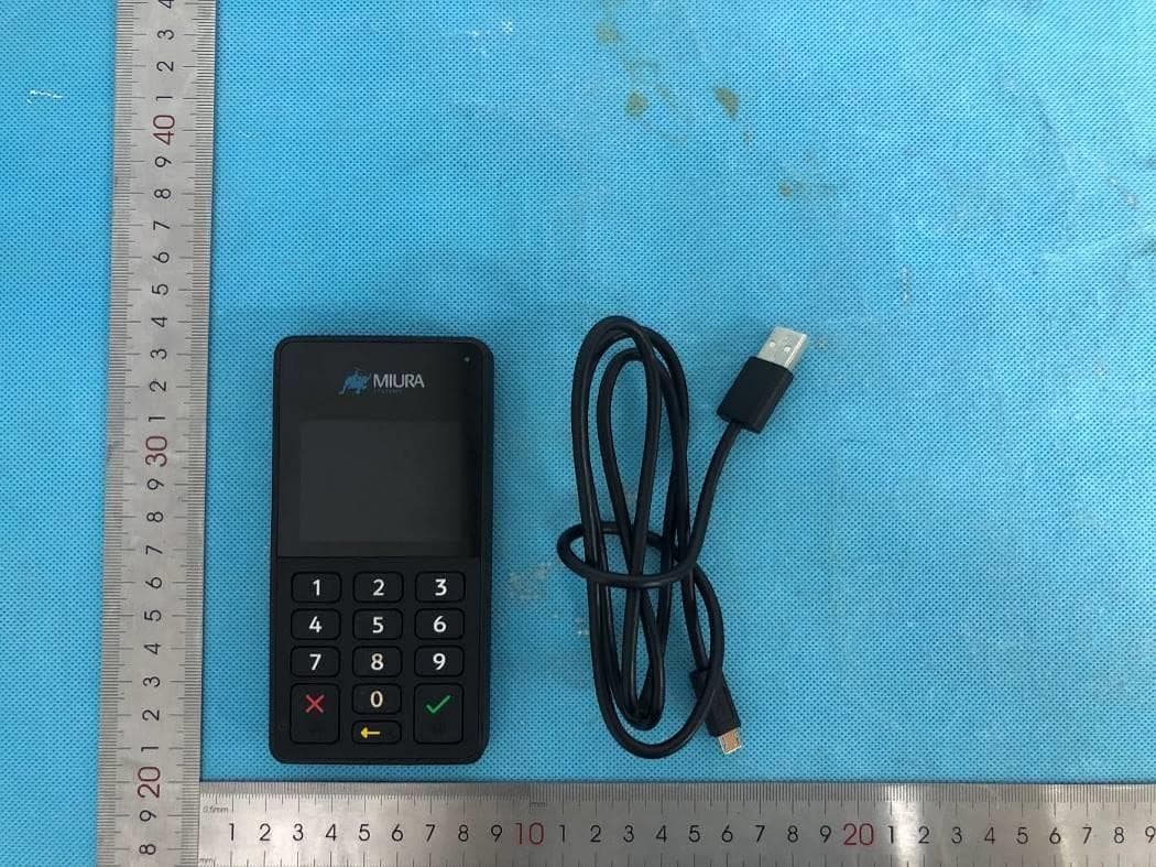
2AO4FM020-2
Jul 06, 2023Mobile Point of Sales terminal
Equipment Class
DTS - Digital Transmission System