2AO4FM020-2Mobile Point of Sales terminal
Miura Systems Ltd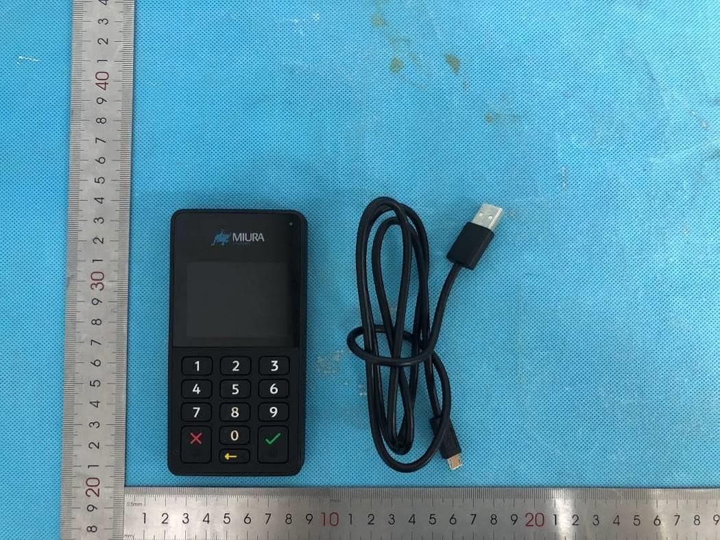
Click to zoom
Application Details
- Equipment Class
- DTS - Digital Transmission System
- Date of Grant
- Jul 06, 2023
- Application Purpose
- Original Equipment
- Date of Application
- Jul 06, 2023
- Equipment Note
- Mobile Point of Sales terminal
- Frequency Range
- 2412.00000000 - 2462.00000000
- Company
- Miura Systems Ltd
- Country
- United Kingdom
Documents & Files
Document Text
Text extracted from the exhibit documents filed with the FCC. Open a document above to read the original.
Users Manual
The terminal automatically performs a full security check every 24 hrs. The terminal can be configured by the application to trigger this security test when the terminal is idle. During this time the Bluetooth will be switched off. The files that failed the security check will be removed from the terminal. 3.8.2 Software Update The software on the terminal can be updated by the application on the smart device. The software update will be transferred to the terminal over the Bluetooth or WiFi, once this is complete the soft- ware update will start. The terminal will indicate if a software update is in progress and will report success/failure. If the software update fails, the operator has to acknowledge the failure by pressing ENTER() to proceed further. In the unlikely event that a software update fails, a Factory-reset (see Revive TM section) may be required to make the terminal operational. Software update in progress. The terminal will display the success or failure message accordingly. 3.9 BACK (X) to return to previous menu as above or OK () continue to return back to idle screen of MPI. BACK (X) to cancel or OK () continue to restart MPI. BACK (X) to cancel the reboot or OK () to reboot the terminal. BACK (X) to cancel the shutdown of the terminal or select OK () to completely shut down the terminal. 3.10 3.10.1 System Tampered If the terminal identifies a tamper, the terminal will immediately close the Payment application abort- ing any transaction in progress. The tamper state is indicated on the display. A Tampered terminal should be returned for investigation. 3.10.2 Ready To Install The terminal will be in Ready To Install state if no application has been installed or has been deleted. A terminal in Ready to Install state should be returned for investigation. 4 Miura products include a Revive TM feature which is activated using a pin-hole reset switch, this is situ- ated next to the power button. Pressing the Revive TM button will trigger a hardware reset, and the terminal will display the Revive Menu. This is best done when there is no external power applied, if external power has been applied the terminal will request to disconnect the external power. The end-user should use this feature if the ower button. The Revive TM Menu has three options, namely:- 4.1 Selecting this option will reboot the terminal resulting in a complete hardware and software reset. 4.2 be- comes unresponsive to power button or is not running as expected and option 1 in the revive menu was unsuccessful in recovering the terminal, terminal unintentional sys- tem restoration. is The terminal will display the success or failure message for the System Restore. If the system Restore process fails, the opera- tor has to acknowledge the failure by pressing the ENTER() key. In the unlikely event that a system restore fails, the terminal may be in an unusable state. The operator 4.3 -user to reset all software and configuration back to the state it was in when the terminal left the factory. This feature should be used if there are any is- process, and the controlling application on the smart device will need to perform any software configuration and key in order to avoid unintentional factory reset operation. ; Factory Reset in progress. The terminal will accordingly display the success or failure message for the Total Factory Reset. If the Total factory reset process fails, the operator has to acknowledge the failure by pressing the EN- TER() key. If the factory reset fails the terminal has to be returned for further investigation. 4.4 The Revive TM button can also be used to activate the terminal's diagnostics facilities. This involves ex- porting operating system log files and running a built-in hardware functional test. It is not envisaged that this will be done by an end-user. The diagnostics state is entered by activating the Revive TM button whilst holding the '0' key. Once the terminal has booted, it will export XXX-XXXXXX-Conf.txt, XXX-XXXXXX-Info.txt and XXX- XXXXXXEvents.txt diagnostic files in the USB Mass Storage Device, where XXX-XXXXXX is the serial number of the terminal. Example contents and format of these files are described in Appendix A: Ex- ample diagnostics Files. When returning a terminal under RMA, these files should be returned as well. Once these files have been retrieved the USB cable can be removed and the terminal automatically starts the functional test, see the Functional Test section. Creating Terminal diagnostic data: This state is notified when the diagnostics state is entered by acti- vating the pin-hole switch. Terminal diagnostics data exported in USB Mass Storage Device: Once the diagnostics log files have been created, the files will be exported in the Mass storage device. The files can be retrieved by con- necting the USB lead to a computer. Unplugging USB lead after this will start functional tests. Failed to export Terminal diagnostics data in Mass storage device: If the terminal fails to export the diagnostics log files in mass storage device, the terminal will display a failure message. The terminal should be identified as a return under warranty and all details of the terminal, and the fault recorded. 5 The Miura Operating System contains a built-in functional test which fully tests the hardware. In order to perform the tests the following are required (and can be obtained from Miura): -swipe and smartcard. . Or alternatively, a modified terminal provided by Miura running specific software with a pre-set Bluetooth address capable of supplying at least 1 Amp. An M020 fast charging cradle -clip (not a sharp object) to activate the pin-hole reset switch. The functional tests are activated when the USB lead is unplugged after the retrieval of the diagnos- tics files from USB Mass Storage Device (MSD). The following are general points for functional tests: ENTER() to continue to next test. Pressing CANCEL(X) when a Test has failed will abort the functional test. CANCEL(X…
Text truncated - open the document above for the full version.
Users Manual
Contents ........................................................................................................................ ................................................................................................ .................................................................. ................................................................................................................. ..................................................................................................... .................................................................................. ..................................................................................................................... .......................................................................................................................... .................................................................................................................. ...................................................................................................... ................................................................................................................ ............................................................................................... ............................................................................................................. ............................................................................................................. ............................................................................................................................ .................................................................................................. .......................................................................................................... ..................................................................................................... .................................................................................................. ................................................................................................................. ................................................................................................................ ......................................................................................................... ............................................................................ .................................................................................................. ............................................................................ ................................................................................................................ ................................................................. ............................................................................................................. ................................................................................................. ........................................................................................................... ............................................................................................... ........................................................................................................ ................................................................................................................. .................................................................................................................. ............................................................... ................................................................................................ ............................................................................................................... .............................................................................. ................................................................................ ....................................................................................... 1 2 3 3.1 This section covers the basic operation and use of the terminal. This covers power on and off, charg- ing, basic Bluetooth connection, transaction PIN entry and terminal maintenance. The logos displayed in this document are configurable. This document assumes that the Miura (MPI) application is loaded and the default logos are still in use. 3.2 3.2.1 Turning the terminal ON To power up, push the power button or plug the terminal into a USB power source. The power-up se- quence starts with the boot logo display. Once the terminal is ready to use, the Bluetooth icon will start to flash or stay solid at the top left corner of the display, depending on whether the terminal has been paired with a smart device. The battery status indicator appears in the top right corner of the display when the terminal is ready to use. 3.2.2 Turning the terminal OFF To switch off, press and hold the power button until the display shows play turns off. Once off, the terminal will not react to any key presses, except Power button and the Revive TM switch. 3.2.3 Sleep The terminal can be put into sleep mode. In this mode the terminal's power consumption is very low (WiFi and Bluetooth is switched off), but when it is woken it will be ready to use within a few seconds. The terminal will enter sleep mode if the power button is briefly pressed, or after a period of inactiv- ity. The terminal will wake on any of the following activities: -Card inserted tripe Card swiped 3.2.4 Charging the Battery The terminal has a rechargeable battery which cannot be removed or replaced. The battery should be charged for at least 3 hours before using the terminal for the first time or if the terminal has not been used for a long time. The battery is charged by plugging the terminal into either a computer or external USB adapter using the USB lead provided. Charging via a USB wall adaptor is faster, but the adaptor must be capable of supplying at least 1A. …
Text truncated - open the document above for the full version.
Attestation Statements
Mario Cosci
External Photos
FCC ID: 2AO4FM020-2 IC: 23677-M0202 External photos FCC ID: 2AO4FM020-2 IC: 23677-M0202 FCC ID: 2AO4FM020-2 IC: 23677-M0202 FCC ID: 2AO4FM020-2 IC: 23677-M0202
ID Label/Location Info
Label & Location back EUT Label Location
Internal Photos
FCC ID: 2AO4FM020-2 IC: 23677-M0202 Internal photos FCC ID: 2AO4FM020-2 IC: 23677-M0202 FCC ID: 2AO4FM020-2 IC: 23677-M0202 FCC ID: 2AO4FM020-2 IC: 23677-M0202 FCC ID: 2AO4FM020-2 IC: 23677-M0202 FCC ID: 2AO4FM020-2 IC: 23677-M0202 FCC ID: 2AO4FM020-2 IC: 23677-M0202 RF Antenna RF Chip FCC ID: 2AO4FM020-2 IC: 23677-M0202 NFC Antenna FCC ID: 2AO4FM020-2 IC: 23677-M0202 FCC ID: 2AO4FM020-2 IC: 23677-M0202 FCC ID: 2AO4FM020-2 IC: 23677-M0202
RF Exposure Info
Hotline: 400-6611-140 Tel: 86-755-27673339 Fax: 86-755-27673332 http://www.tct-lab.com SAR TEST REPORT FCC ID. ............................ : 2AO4FM020-2 Test Report No. ............... : TCT230522E020 Date of issue ................... : May 30, 2023 Testing laboratory .......... : SHENZHEN TONGCE TESTING LAB Testing location/ address: 2101 & 2201, Zhenchang Factory Renshan Industrial Zone, Fuhai Subdistrict, Bao'an District, Shenzhen, Guangdong, 518103, People's Republic of China Applicant's name ............ : Miura Systems Ltd Address ........................... : Unit 3, Cliveden Office Village, Lancaster Road, Cressex Industrial Estate, High Wycombe, HP12 3YZ, United Kingdom Manufacturer's name ... : Miura Systems Ltd Address ........................... : Unit 3, Cliveden Office Village, Lancaster Road, Cressex Industrial Estate, High Wycombe, HP12 3YZ, United Kingdom Factory .......................... : Jabil Vietnam Company Limited Address ........................... : Lot I-8 SaiGon Hitech Park, Long Thanh My ward, Thu Duc city, Ho Chi Minh city, Vietnam Test item description ..... : Mobile Point of Sales terminal Trade Mark ...................... : Miura Systems Ltd Model/Type reference..... : M020,M021 SAR Max. Values..............: 0.16 W/Kg (1g) for Body-worn Date of receipt of test item ......................................... : May 22, 2023 Date (s) of performance of test ................................... : May 22, 2023 - May 30, 2023 Tested by (+signature) ... : Una LI Check by (+signature) .... : Beryl Zhao Approved by (+signature): Tomsin General disclaimer: This report shall not be reproduced except in full, without the written approval of SHENZHEN TONGCE TESTING LAB. This document may be altered or revised by SHENZHEN TONGCE TESTING LAB personnel only, and shall be noted in the revision section of the document. The test results in the report only apply to the tested sample. Report No.: TCT230522E020 Page 2 of 64 Hotline: 400-6611-140 Tel: 86-755-27673339 Fax: 86-755-27673332 http://www.tct-lab.com TABLE OF CONTENTS 1. General Product Information .................................................................. 3 1.1. EUT description ................................................................................................................................. 3 1.2. Model(s) list ....................................................................................................................................... 3 2. Test standard ........................................................................................... 4 2.1. Facilities and Accreditations ........................................................................................................... 4 2.2. Location.............................................................................................................................................. 4 2.3. Environment Condition: ................................................................................................................... 4 3. Test Result Summary .............................................................................. 5 4. RF Exposure Limit ................................................................................... 6 5. SAR Measurement System Configuration ............................................. 7 5.1. SAR Measurement Set-up ................................................................................................................ 7 5.2. E-field Probe ...................................................................................................................................... 8 5.3. Phantom ............................................................................................................................................. 8 5.4. Device Holder .................................................................................................................................... 9 5.5. Data Storage and Evaluation ......................................................................................................... 10 5.6. Position of the wireless device in relation to the phantom ........................................................ 11 5.7. Tissue Dielectric Parameters ......................................................................................................... 14 5.8. Tissue-equivalent Liquid Properties ............................................................................................. 15 5.9. System Check .................................................................................................................................. 16 6. Measurement Procedure ....................................................................... 17 7. Conducted Output Power ...................................................................... 20 8. Exposure Position Consideration ........................................................ 22 8.1. EUT Antenna Location .................................................................................................................... 22 8.2. Test Position Consideration .......................................................................................................... 22 9. SAR Test Results Summary .................................................................. 23 9.1. Body-Worn 1g SAR Data ................................................................................................................ 23 9.2. Measurement Uncertainty (450MHz-3GHz) ................................................................................... 24 9.3. Test Equipment List ........................................................................................................................ 26 10. System Check Results .......................................................................... 27 11. SAR Test Data ........................................................................................ 29 Appendix C: Probe Calibration Ce…
Text truncated - open the document above for the full version.
Test Report
Application Bluetooth Zigbee WLAN (IEEE 802.11 b/g/n) ISM 2.4GHz Wireless Devices Features Helical Structure Size (6.0*2.0*1.2mm 3 ) Easy Optimizing with external lumped matching components SMT Available under Pb-free Condition RoHSCompliant DATASHEET DocumentDatasheet TypeMultilayer Chip Antenna Application2.4GHz Part No.ALA621C4 Revision6.0 Notes The contents of this datasheet are subject to change without notice. Please confirm the specifications and delivery conditions when placing your order. AMOTECH AMOTECH Co., Ltd. Datasheet / Multilayer Chip Antenna / 2.4GHz ALA621C4 (Rev 6.0) 2 Rev. NoDateTitleContentsPage 6’10.01.19FormatChangeddocument format Table of Content Revision History 1.Specifications 3 1.1 Electrical Specifications 3 1.2 Mechanical Specifications 3 1.3 Appearance and Material 3 2. PCB Design for Test 4 2.1 Evaluation BoardDimension 4 2.2 PCB Design Guide 4 3. Measurement Result 5 3.1 Typical Measurement Result (VSWR/RL,Smithchart) 5 3.2 Typical Measurement Result(Gain, Radiation Pattern) 6 4. Reliability 7 5. Soldering Reflow Profile 7 6. Packaging 8 6.1 Carrier Tape Dimension 8 6.2 PackagingQuantity 8 6.3 Packaging Label 8 Datasheet / Multilayer Chip Antenna / 2.4GHz ALA621C4 (Rev 6.0) 3 NoItemSpec.Remark 1Frequency Range [GHz]2.4 ~2.485 2VSWRMax 3.0:1 3Peak Gain [dBi]typ. 3.5 4Total Avg. Gain [dBi]typ. -0.25 5Efficiency [%]typ. 94 6PolarizationLinear 7Impedance [Ω]Nominal 50 The results are measured on the 10x43mm 2 evaluation board(EVB). See Page 6. for more detail gain parameter NoItemSpec.Remark 1Dimensions (LxWxH)6.0x2.0x1.2 mm 3 2Unit Weighttyp. 46 mg 3Operating Temperature-35 ~ +85 °C 1.1 Electrical Specifications 1.2 Mechanical Specifications NoItemFunctionMaterial ①External ElectrodeSoldering, Input PortAg/Ni/Sn ② Direction indexIndication of Ceramic ③Model No. index-Ceramic ④Ceramic Body-Ceramic ⑤External ElectrodeSolderingAg/Ni/Sn 1.3 Appearance & Material 1. Specifications ③ ④ ⑤ ② ① 0.6±0.2 6.0±0.3 2.0±0.2 Side 1.2±0.2 (unit : mm) A40600 Datasheet / Multilayer Chip Antenna / 2.4GHz ALA621C4 (Rev 6.0) 4 2.1 Evaluation Board Dimension 2.2 PCB Design Guide 2. PCB Design for Test NoPin Assignment ① Feeding ②N.C Matching Component [unit : mm] Evaluation board size ~ 10x43 Fill Cut Area (GND Clearance) ~ 10x13 [PCB Solder Land] 50 Ohm Feeding Line SMA Connector Chip Antenna GND Matching Stage [Unit : mm] 7.0 1.1 2.2 4.8 ① ② Datasheet / Multilayer Chip Antenna / 2.4GHz ALA621C4 (Rev 6.0) 5 3.1 Typical Measurement Result (VSWR/RL, Smithchart) 3. Measurement Result The results are measured on the 10x43mm 2 evaluation board(EVB). NoMatching Value ①N.C ②2.7 nH ③ 2.2 nH ③① ② Datasheet / Multilayer Chip Antenna / 2.4GHz ALA621C4 (Rev 6.0) 6 [Azimuth plane @2.45GHz ] [Elevation1 plane @2.45GHz ] [Elevation2 plane @2.45GHz ] [3D Radiation Pattern] 3.2 Typical Measurement Result (Gain, Radiation Pattern) x y z -y Azimuth E1 E2 Peak Gain (dBi) Avg. Gain (dBi) Total Avg. Gain (dBi) Efficiency (%) Azimuth 2.60.7 -0.2594 Elevation 1 3.5-0.6 Elevation 2 2.0-1.7 Datasheet / Multilayer Chip Antenna / 2.4GHz ALA621C4 (Rev 6.0) 7 NoItemTest ConditionTest Requirements 1 Adhesive Strength of Termination 1.Applied force on SMT chip till detached point from PCB. 1. No mechanical damage by applied force 2. Strength (F) > 5 kgf 2 Thermal Shock (Cycle) 1. Step 1 : -40 ±3°C, 30 min Step 2 : +125 ±3°C, 30 min 2. Number of cycle : 30 1. No visual damage 2. Within electric spec (VSWR) 3 High Temperature Resistance 1. Temperature : +125 ±5°C 2. Time : 1000 ±24 hrs 1. No visual damage 2. Within electric spec (VSWR) 4 Low Temperature Resistance 1. Temperature : -40 ±5°C 2. Time : 1000 ±24 hrs 1. No visual damage 2. Within electric spec (VSWR) 5Humidity 1. Humidity : 85 % RH Temperature : +85 ±3°C 2. Time : 1000 ±24 hrs 1. No visual damage 2. Within electric spec (VSWR) F SMD PAD PCB 4. Reliability 5. Soldering Reflow Profile Datasheet / Multilayer Chip Antenna / 2.4GHz ALA621C4 (Rev 6.0) 8 ItemSpec.ItemSpec.ItemSpec. A02.30±0.10P04.00 ±0.10E1.75±0.10 B06.40±0.10P14.00 ±0.10F7.50±0.10 K01.35±0.10P22.00 ±0.10W16.00±0.30 D01.55±0.05--t0.30±0.05 Item QuantityDimension Reel2,000eaΦ7” * 12mm Inner Box6,000ea (3 reel)185 * 185 * 68 (mm 3 ) Outer Box130,000ea (5 Inner Box)375 * 200 * 205 (mm 3 ) Outer Box260,000ea (10 Inner Box)390 * 375 * 205 (mm 3 ) 6.1 Carrier Tape Dimension 6.2 Packaging Quantity 6.3 Packaging Label 6. Packaging AMOTECH Co., Ltd. 5BL-1Lot, 617, Namchon-Dong, Namdong-Gu, Incheon, Korea Multilayer Chip Antenna P/N : ALA621C4 Lot No : Quantity : 2,000 pcs Date : 2010/01/19
Test Report
Report No.: NTC2304454FV00 Dongguan Nore Testing Center Co., Ltd. Address: Building D, Gaosheng Science and Technology park, Hongtu road, Nancheng district, Dongguan city, Guangdong province, China Web: www.ntc-c.com Tel:+86-769-2202 2444 Fax:+86-769-2202 2799 Page 1 of 47 FCC RADIO TEST REPORT Applicant......................... : Miura Systems Ltd Address........................... : Unit 3, Cliveden Office Village, Lancaster Road, Cressex Industrial Estate, High Wycombe, HP12 3YZ, United Kingdom Manufacturer.................... : Miura Systems Ltd Address........................... : Unit 3, Cliveden Office Village, Lancaster Road, Cressex Industrial Estate, High Wycombe, HP12 3YZ, United Kingdom Factory............................. : Jabil Vietnam Company Limited Address............................ : Lot I-8 SaiGon Hitech Park, Long Thanh My ward, Thu Duc city, Ho Chi Minh city, Vietnam Product Name................... : Mobile Point of Sales terminal Brand Name..................... : Miura Systems Ltd Model No. ....................... : M021, M020 (For model difference refer to section 2.) FCC ID............................. : 2AO4FM020-2 Measurement Standard....... : 47 CFR FCC Part 15, Subpart C (Section 15.247) Receipt Date of Samples.... : April 24, 2023 Date of Tested.................. : April 24, 2023 to May 25, 2023 Date of Report.................. : June 29, 2023 This report shows that above equipment is technically compliant with the requirements of the standards above. All test results in this report apply only to the tested sample(s). Without prior written approval of Dongguan Nore Testing Center Co., Ltd, this report shall not be reproduced except in full. Prepared by Rose Hu / Project Engineer Approved by Iori Fan / Authorized Signatory Report No.: NTC2304454FV00 Page 2 of 47 Table of Contents 1. Summary of Test Result ...................................................................................................................................... 4 2. General Description of EUT ................................................................................................................................ 5 3. Test Channels and Modes Detail ........................................................................................................................ 8 4. Configuration of EUT ........................................................................................................................................... 8 5. Modification of EUT ............................................................................................................................................. 8 6. Description of Support Device ............................................................................................................................. 9 7. Test Facility and Location ................................................................................................................................. 10 8. Applicable Standards and References .............................................................................................................. 11 9. Deviations and Abnormalities from Standard Conditions ................................................................................. 11 10. Test Conditions ............................................................................................................................................... 12 11. Measurement Uncertainty ............................................................................................................................... 13 12. Sample Calculations ....................................................................................................................................... 13 13. Test Items and Results ................................................................................................................................... 15 13.1 Conducted Emissions Measurement ............................................................................................................ 15 13.2 Maximum Conducted Output Power Measurement ...................................................................................... 19 13.3 6dB Bandwidth Measurement ....................................................................................................................... 21 13.4 Power Spectral Density Measurement ......................................................................................................... 25 13.5 Band Edge and Conducted Spurious Emissions Measurement ................................................................... 29 13.6 Radiated Spurious Emissions and Restricted Bands Measurement ............................................................ 34 13.7 Antenna Requirement ................................................................................................................................... 46 14. Test Equipment List......................................................................................................................................... 47 Report No.: NTC2304454FV00 Page 3 of 47 Revision History Report Number Description Issued Date NTC2304454FV00 Initial Issue 2023-06-29 Report No.: NTC2304454FV00 Page 4 of 47 1. Summary of Test Result FCC Rules Description of Test Result Remarks §15.207 (a) AC Power Conducted Emission PASS --- §15.247(b)(3) Maximum Conducted Output Power PASS --- §15.247(a)(2) 6dB Bandwidth PASS --- §15.247(e) Power Spectral Density PASS --- §15.247(d) Band Edge and Conducted Spurious Emissions PASS --- §15.247(d),§15.209, §15.205 Radiated Spurious Emissions and Restricted Bands PASS --- §15.203 Antenna Requirement PASS --- Report No.: NTC2304454FV00 Page 5 of 47 2. General Description of EUT Product Information Product Name: Mobile Point of Sales terminal Main Model Name: M021 Additional Model Name: M020 Model Difference: Both M020 and M021 have the same design in circuit diagram and PCB layout, and the…
Text truncated - open the document above for the full version.
Test Setup Photos
FCC ID: 2AO4FM020-2 IC: 23677-M0202 Test Photo Radiated emission (Below 30MHz) FCC ID: 2AO4FM020-2 IC: 23677-M0202 Radiated emission (30-1000MHz) FCC ID: 2AO4FM020-2 IC: 23677-M0202 Radiated emission (Above 1000MHz) FCC ID: 2AO4FM020-2 IC: 23677-M0202 Conducted Emission
Test Setup Photos
Page 1 of 2 Appendix B: Photographs of EUT FCC ID: 2AO4FM020-2 Product: Mobile Point of Sales terminal Model: M021 Test Setup Photos Body worn – Back (0mm) Body worn – Front (0mm) Page 2 of 2 Body worn – Top (0mm) Body worn – Left (0mm)
Contact Information
Applicant
Mario Cosci(Test & Certification Manager)
Technical Contact
Non-Technical Contact
Dongguan NTC Co., Ltd.Jees hong
[email protected]86-0769-22022444
Test Firm
Dongguan NTC CO., Ltd.Jees Hong
[email protected]+86-769-22022444
Technical Specifications
| # | Rule Parts | Frequency Range | Power Output |
|---|---|---|---|
| 1 | 15C | 2.41 GHz - 2.46 GHz | 130.50 mW |
Other Applications from Miura Systems Ltd
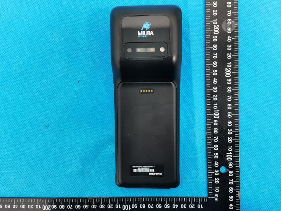
2AO4FMASP01
Jul 17, 2024MASP01
Equipment Class
PCB - PCS Licensed Transmitter
2AO4FM010-3
Jan 12, 2020Portable payment terminal
Equipment Class
DSS - Part 15 Spread Spectrum Transmitter