2BATE-FC-200Wireless Gaming Headset
Shenzhen wei bo technology co., LTD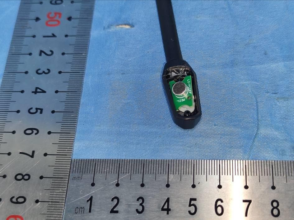
Click to zoom
Application Details
- Equipment Class
- DSS - Part 15 Spread Spectrum Transmitter
- Date of Grant
- Aug 03, 2024
- Application Purpose
- Original Equipment
- Date of Application
- Aug 03, 2024
- Equipment Note
- Wireless Gaming Headset
- Frequency Range
- 2402.00000000 - 2480.00000000
- Country
- China
Documents & Files
Document Text
Text extracted from the exhibit documents filed with the FCC. Open a document above to read the original.
Users Manual
This device complies with Part 15 of the FCC rules. Operation is subject to the following two conditions: 1) this device may not cause harmful interference, and 2) this device must accept any interference received, including interference that may cause undesired operation.Note: This equipment has been tested and found to comply with the limits for a ClassB digital device, pursuant to part 15 of the FCC Rules. These limits are designed toprovide reasonable protection against harmful interference in a residential installation.This equipment generates uses and can radiate radio frequency energy and, if not installed and used in accordance with the instructions, may cause harmful interference to radio communications. However, there is no guarantee that interference will not occur in particular installation. If this equipment does cause harmful interference to radio or television reception, which can be determined by turning the equipment off and on, the user is encouraged to try to correct the interference by one or more of the following measures:--Reorient or relocate the receiving antenna.--Increase the separation between the equipment and receiver.--Connect the equipment into an outlet on a circuit different from that to which the receiver is connected.--Consult the dealer or an experienced radio/TV technician for help.Changes or modifications not expressly approved by the party responsible for compliance could void the user’s authority to operate the equipment.Radiation Exposure StatementThis device complies with RF radiation exposure limits set forth for an uncontrolled environment. This transmitter must not be co-located or operating in conjunction with any other antenna or transmitter. 8
Attestation Statements
- Shenzhen wei bo technology co., LTD - Federal Communications Commission Authorization and Evaluation Division Equipment Authorization Branch 7435 Oakland Mills Road Columbia, MD 21046 02.08.2024 U.S. Agent Designation [ Shenzhen wei bo technology co., LTD] acknowledges their consent for the following contact located in the United States to act as their agent for service of process for the equipment for which authorization is sought (FCC ID: 2BATE-FC-200 Name and company of U.S. agent: 【UUX GROUP INC】 Physical U.S. address of agent: 【36 South 18th Avenue, Suite A Brighton, CO USA 80601】 FRN of U.S. agent: 【0033701590】 Email address of U.S. agent: 【[email protected]】 [UUX GROUP INC] acknowledges their obligation to accept service of process on behalf of [ Shenzhen wei bo technology co., LTD ]. Shenzhen wei bo technology co., LTD with the FRN [0033641028] accepts its obligation to maintain an agent for service of process in the United States for no less than one year after either the grantee has permanently terminated all marketing and importation of the applicable equipment within the U.S., or the conclusion of any Commission-related administrative or judicial proceeding involving the equipment, whichever is later. By signing this form, we confirm the above and that we are aware of the application requirements listed under § 2.911(d)(7). The information provided in this letter is based on the referenced rule parts of Title 47 of the CFR as well as KDB 986446 D01. An expiration date for this letter does not exist. In case the U.S. agent changes, the grantee is obligated to notify the FCC within 30 days via the granting TCB. Sincerely, Signature Wei Chen Manager Shenzhen wei bo technology co., LTD Signature Jack Fu Manager UUX GROUP INC 48_[mo del] US_Agent_2.911(d)(7) - U, V05
ID Label/Location Info
FCC ID: 2BATE-FC-200
Internal Photos
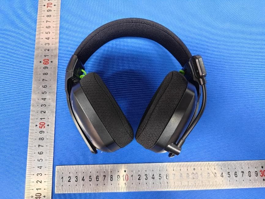
FCC ID: 2BATE-FC-200 Photo 1 Photo 2 FCC ID: 2BATE-FC-200 Photo 3 Photo 4 FCC ID: 2BATE-FC-200 Photo 5 Photo 6 FCC ID: 2BATE-FC-200 Photo 7 Photo 8 FCC ID: 2BATE-FC-200 Photo 9 Photo 10 BT ANT FCC ID: 2BATE-FC-200 Photo 11 Photo 12 FCC ID: 2BATE-FC-200 Photo 13 Photo 14 FCC ID: 2BATE-FC-200 Photo 15 Photo 16 FCC ID: 2BATE-FC-200 Photo 17 Photo 18
RF Exposure Info
RF Exposure evaluation FCC ID: 2BATE-FC-200 Applicable Standard According to §1.1307(b)(1), systems operating under the provisions of this section shall be operated in a manner that ensures that the public is not exposed to radio frequency energy level in excess of the Commission’s guidelines. According to §1.1310 and §2.1093 RF exposure requirement KDB447498 v06: Mobile and Portable Devices RF Exposure Procedures and Equipment Authorization Policies 1.1. Requirement According to KDB447498 D01 General RF Exposure Guidance v06 Section 4.3.1 Standalone SAR test exclusion considerations: “Unless specifically required by the published RF exposure KDB procedures, standalone 1-g head or body and 10-g extremity SAR evaluation for general population exposure conditions, by measurement or numerical simulation, is not required when the corresponding SAR Test Exclusion Threshold condition, listed below, is satisfied. These test exclusion conditions are based on source-based time-averaged maximum conducted output power of the RF channel requiring evaluation, adjusted for tune-up tolerance, and the minimum test separation distance required for the exposure conditions.22 The minimum test separation distance is determined by the smallest distance from the antenna and radiating structures or outer surface of the device, according to the host form factor, exposure conditions and platform requirements, to any part of the body or extremity of a user or bystander (see 5) of section 4.1). To qualify for SAR test exclusion, the test separation distances applied must be fully explained and justified by the operating configurations and exposure conditions of the transmitter and applicable host platform requirements, typically in the SAR measurement or SAR analysis report, according to the required published RF exposure KDB procedures. When no other RF exposure testing or reporting is required, a statement of justification and compliance must be included in the equipment approval, in lieu of the SAR report, to qualify for the SAR test exclusion. When required, the device specific conditions described in the other published RF exposure KDB procedures must be satisfied before applying these SAR test exclusion provisions; for example, handheld PTT two-way radios, handsets, laptops & tablets etc.23 “ [(max. power of channel, including tune-up tolerance, mW)/ (min. test separation distance, mm)] · [√f (GHz)] ≤ 3.0 for 1-g SAR and ≤ 7.5 for 10-g extremity SAR, where: • f (GHz) is the RF channel transmit frequency in GHz • Power and distance are rounded to the nearest mW and mm before calculation • The result is rounded to one decimal place for comparison • 3.0 and 7.5 are referred to as the numeric thresholds in the step 2 below The test exclusions are applicable only when the minimum test separation distance is ≤ 50 mm and for transmission frequencies between 100 MHz and 6 GHz. When the minimum test separation distance is < 5 mm, a distance of 5 mm according to 5) in section 4.1 is applied to determine SAR test exclusion. 1.2. Manufacturing tolerance BR - EDR GFSK Channel Channel 00 Channel 39 Channel 78 Target (dBm) -2.0 -2.0 -2.0 Tolerance ±(dB) 1.0 1.0 1.0 π/4DQPSK Channel Channel 00 Channel 39 Channel 78 Target (dBm) -1.0 -1.0 -1.0 Tolerance ±(dB) 1.0 1.0 1.0 8DPSK Channel Channel 00 Channel 39 Channel 78 Target (dBm) -1.0 -1.0 -1.0 Tolerance ±(dB) 1.0 1.0 1.0 2.4GHz mode 2.4GHz GFSK Channel Channel 00 Channel 19 Channel 39 Target (dBm) 0 0 0 Tolerance ±(dB) 1.0 1.0 1.0 Page 2 of 2 2. E v a l u a t i o n R e s u l t Evaluation Results Band/Mode f (GHz) Antenna Distance (mm) Max.RF output power (including tune-up tolerance) SAR Test Exclusion Threshold SAR Test Exclusion dBm mW BR-EDR 2.45 5 0 1.000 0.3<3 Yes 2.4GHz SRD 2.45 5 1 1.259 0.4<3 Yes 3. C o n c l u s i o n The measurement results comply with the FCC Limit per 47 CFR 2.1093 for the uncontrolled RF Exposure and SAR Exclusion Threshold per KDB 447498 v06 .....................End of Report.........................
Test Report
Page 1 of 38 Report No.: AiTDG-240719006W1 Guangdong Asia Hongke Test Technology Limited B1/F, Building 11, Junfeng Industrial Park, Chongqing Road, Heping Community, Fuhai Street, Bao'an District, Shenzhen, Guangdong, China. TEST REPORT Client Information: Applicant: Shenzhen wei bo technology co., LTD Applicant add.: Room 601, Tower A, Yousuowei Building, No. 2000, Jiaxian Road, Bantian street, Longgang District, Shenzhen Manufacturer: Dongguan Huawei Technology Co., Ltd Manufacturer add.: Room 101, Building 1, No. 39 Yongping Lane, Dongshan, Qishi Town, Dongguan City, Guangdong Province Product Information: Product Name: Wireless Gaming Headset Model No.: FC-200 Series Model: Refer to Section 4(General Information) Brand Name: N/A Test samples.: AiTDG-240719006-1 FCC ID: 2BATE-FC-200 Applicable standards: FCC CFR Title 47 Part 15 Subpart C Section 15.247 Prepared By: Guangdong Asia Hongke Test Technology Limited B1/F, Building 11, Junfeng Industrial Park, Chongqing Road, Heping Community, Fuhai Street, Bao'an District, Shenzhen, Guangdong, China Tel.: +86 0755-230967639 Fax.: +86 0755-230967639 Date of Receipt: July 15, 2024 Date of Test: July 15, 2024 ~ July 18, 2024 Date of Issue: July 19, 2024 Test Result: Pass This device described above has been tested by Guangdong Asia Hongke Test Technology Limited and the test results show that the equipment under test (EUT) is in compliance with the FCC requirements. And it is applicable only to the tested sample identified in the report. Note: This report shall not be reproduced except in full, without the written approval of Guangdong Asia Hongke Test Technology Limited, this document may be altered or revised by Guangdong Asia Hongke Test Technology Limited, personal only, and shall be noted in the revision of the document. This test report must not be used by the client to claim product endorsement. Reviewed by: Approved by: Leon.yi Sean She Page 2 of 38 Report No.: AiTDG-240719006W1 Guangdong Asia Hongke Test Technology Limited B1/F, Building 11, Junfeng Industrial Park, Chongqing Road, Heping Community, Fuhai Street, Bao'an District, Shenzhen, Guangdong, China. 1 Contents Page COVER PAGE 1 CONTENTS...................................................................................................................................................... 2 2 TEST SUMMARY ............................................................................................................................................ 4 2.1 Statement of the Measurement Uncertainty ....................................................................................... 4 2.2 Measurement Uncertainty ................................................................................................................... 4 3 TEST FACILITY ............................................................................................................................................... 5 3.1 Deviation from standard ...................................................................................................................... 5 3.2 Abnormalities from standard conditions .............................................................................................. 5 3.3 Test Location ....................................................................................................................................... 5 4 GENERAL INFORMATION ............................................................................................................................. 6 4.1 Test frequencies .................................................................................................................................. 7 4.2 EUT Peripheral List ............................................................................................................................. 8 4.3 Test Peripheral List .............................................................................................................................. 8 4.4 TEST METHODOLOGY ...................................................................................................................... 9 4.5 Description of Test Modes ................................................................................................................. 10 5 EQUIPMENT USED DURING TEST ............................................................................................................. 11 6 TEST RESULTS AND MEASUREMENT DATA ........................................................................................... 12 6.1 Antenna requirement ......................................................................................................................... 12 6.2 Peak Power Measurement ................................................................................................................ 13 6.3 Frequency Separation and 20 dB Bandwidth ................................................................................... 15 6.4 Number of Hopping Frequency ......................................................................................................... 17 6.5 Time of Occupancy (Dwell Time) ...................................................................................................... 18 6.6 Conducted Spurious Emissions and Band Edges Test ..................................................................... 20 6.7 Radiated Emissions and Radiation Restricted band Measurement ................................................. 22 6.8 Conducted Emissions ........................................................................................................................ 34 6.9 Pseudorandom frequency hopping sequence .................................................................................. 37 7 TEST SETUP PHOTOGRAPHS OF EUT ..................................................................................................... 38 8 EXTERNAL PHOTOGRAPHS OF EUT ...............................................…
Text truncated - open the document above for the full version.
Test Report
2.4GHz3216ChipAntenna:3216F245M02 第 1 页共 10 页 咏成國際科技有限公司電話:13530576606 RAINInternationalTechnologyCo.,Ltd.TEL:13530576606 3216Chipantenna ForBluetooth/WLANApplicationsd P/N:RANT3216F245M02 Dimension(mm) L3.23±0.20 W1.66±0.20 T1.23±0.20 2.4GHz3216ChipAntenna:3216F245M02 第 2 页共 10 页 咏成國際科技有限公司電話:13530576606 RAINInternationalTechnologyCo.,Ltd.TEL:13530576606 PartNumberInformation RANT 3216F245M02 ABCDEF A ProductSeriesAntenna BDimensionLxW3.2X1.6mm(+-0.2mm) CMaterialHighKmaterial D WorkingFrequency2.4~2.5GHz E FeedingmodeMonopole&SingleFeeding F AntennatypeType=02 1.ElectricalSpecification Specification PartNumberRANT3216F245M02 CentralFrequency2450MHz Bandwidth100(Min.)MHz ReturnLoss-6.5(Max)dB PeakGain3dBi Impedance50Ohm OperatingTemperature -40~+85°C MaximumPower4W ResistancetoSolderingHeats 10(@260 °C ) sec. PolarizationLinear AzimuthBeamwidthOmni-directional TerminationCu/Sn(Leadless) Remark:Bandwidth&PeakGainwasmeasuredunderevaluationboardofnextpage 2.4GHz3216ChipAntenna:3216F245M02 第 3 页共 10 页 咏成國際科技有限公司電話:13530576606 RAINInternationalTechnologyCo.,Ltd.TEL:13530576606 2.RecommendedPCBPattern EvaluationBoardDimension Unit:mm SuggestedMatchingCircuit 2.4GHz3216ChipAntenna:3216F245M02 第 4 页共 10 页 咏成國際科技有限公司電話:13530576606 RAINInternationalTechnologyCo.,Ltd.TEL:13530576606 LayoutDimensionsinClearancearea ( Size=5.2*5.0mm ) 50ohmtransmissionLine MatchingCircuit FootPrint(Unit:mm) 2.4GHz3216ChipAntenna:3216F245M02 第 5 页共 10 页 咏成國際科技有限公司電話:13530576606 RAINInternationalTechnologyCo.,Ltd.TEL:13530576606 3.MeasurementResults ReturnLoss 2.4GHz3216ChipAntenna:3216F245M02 第 6 页共 10 页 咏成國際科技有限公司電話:13530576606 RAINInternationalTechnologyCo.,Ltd.TEL:13530576606 RadiationPattern Y X Z Efficiency 2400MHz55.21% 2450MHz66.45% 2500MHz57.53% 2.4GHz3216ChipAntenna:3216F245M02 第 7 页共 10 页 咏成國際科技有限公司電話:13530576606 RAINInternationalTechnologyCo.,Ltd.TEL:13530576606 4.ReliabilityandTestCondictions ITEMREQUIREMENTSTESTCONDITION Solderability 1.Wettingshallexceed90%coverage 2.Novisiblemechanicaldamage TEMP(°C) 230°C 4±1sec. 150 °C 60sec Pre-heatingtemperature:150°C/60sec. Soldertemperature:230±5°C Duration:4±1sec. Solder:Sn-Ag3.0-Cu0.5 Fluxforleadfree:rosin Solderheat Resistance 1.Novisiblemechanicaldamage 2.CentralFreq.change:within±6% TEMP(°C) 260°C 10±0.5sec. 150°C 60sec Pre-heatingtemperature:150°C/60sec. Soldertemperature:260±5°C Duration:10±0.5sec. Solder:Sn-Ag3.0-Cu0.5 Fluxforleadfree:rosin Component Adhesion (Pushtest) 1.Novisiblemechanicaldamage Thedeviceshouldbereflow soldered(230±5°Cfor10sec.)toatinned coppersubstrateAdynometerforce gaugeshouldbeappliedthesideofthe component.Thedevicemustwith-ST-F 0.5Kgwithoutfailureofthetermination attachedtocomponent. Component Adhesion (Pulltest) 1.Novisiblemechanicaldamage Insert10cmwireintotheremainingopen eyebend,theendsofevenwirelengths upwardandwindtogether. Terminalshallnotberemarkably damaged. 2.4GHz3216ChipAntenna:3216F245M02 第 8 页共 10 页 咏成國際科技有限公司電話:13530576606 RAINInternationalTechnologyCo.,Ltd.TEL:13530576606 Thermalshock 1.Novisiblemechanicaldamage 2.CentralFreq.change:within±6% Phase Temperature( °C ) Time(min) 1 +85±5°C 30±3 2 RoomWithin Temperature3sec 3 -40±2 °C 30±3 4 RoomWithin Temperature3sec +85 °C =>30±3min -40 °C =>30±3min Testcycle:10cycles Thechipshallbestabilizedatnormal conditionfor2~3hoursbefore measuring. Resistanceto High Temperature 1.Novisiblemechanicaldamage 2.CentralFreq.change:within±6% 3.Nodisconnectionorshortcircuit. Temperature:85±5 °C Duration:1000±12hrs Thechipshallbestabilizedatnormal conditionfor2~3hoursbefore measuring. Resistanceto Low Temperature 1.Novisiblemechanicaldamage 2.CentralFreq.change:within±6% 3.Nodisconnectionorshortcircuit. Temperature:-40±5 °C Duration:1000±12hrs Thechipshallbestabilizedatnormal conditionfor2~3hoursbefore measuring. Humidity 1.Novisiblemechanicaldamage 2.CentralFreq.change:within±6% 3.Nodisconnectionorshortcircuit. Temperature:40±2°C Humidity:90%to95%RH Duration:1000±12hrs Thechipshallbestabilizedatnormal conditionfor2~3hoursbefore measuring. 5.SolderingandMounting Mildlyactivatedrosinfluxesarepreferred.Theminimumamountofsoldercan leadtodamagefromthestressescausedbythedifferenceincoefficientsof expansionbetweensolder,chipandsubstrate.Theterminationsaresuitable forallwaveandre-flowsolderingsystems.Ifhandsolderingcannotbe avoided,thepreferredtechniqueistheutilizationofhotairsolderingtools. ReflowSoldering PRE-HEATING 250~260 230 180 150 SOLDERING 10smax. NATURAL COOLING IronSoldering PRE-HEATINGSOLDERINGNATURAL COOLING 60~120s30~60s TIME(sec.) TIME(sec.) Recommendedtemperatureprofilesforre-flowsolderinginFigure1. Productsattachmentwithasolderingironisdiscouragedduetotheinherent processcontrollimitations.Intheeventthatasolderingironmustbe employedthefollowingprecautionsarerecommended. within3s 350 150 Over60s Gradualcooling 300 T E M P E R A T U R E ( ° C ) T E M P E R A T U R E ( ° C ) 2.4GHz3216ChipAntenna:3216F245M02 第 9 页共 10 页 咏成國際科技有限公司電話:13530576606 RAINInternationalTechnologyCo.,Ltd.TEL:13530576606 1.593.511.80 ‧Preheatcircuitandproductsto150°C ‧Nevercontacttheceramicwiththeirontip ‧Usea20wattsolderingironwithtipdiameterof1.0mm ‧280°Ctiptemperature(max) ‧1.0mmtipdiameter(max) ‧Limitsolderingtimeto3sec. 6.PackagingInformation TapeSpecification: ReelSpecification:(7’’,Φ180mm) 2.4GHz3216ChipAntenna:3216F245M02 第 10 页共 10 页 咏成國際科技有限公司電話:13530576606 RAINInternationalTechnologyCo.,Ltd.TEL:13530576606 TapeWidth(mm)A(mm)B(mm)C(mm)D(mm)Chip/Reel(pcs) 89.0±0.560±213.5±0.5178±23000 7.StorageandTransportationInformation StorageConditions Tomaintainthesolderabilityofterminalelectrodes: 1.Temperatureandhumidityconditions:-10~40°Cand30~70%RH. 2.Recommendedproductsshouldbeusedwithin6monthsfromthetimeof delivery. 3.Thepackagingmaterialshouldbekeptwherenochlorineorsulfurexists intheair. TransportationConditions 1.Productsshouldbehandledwithcaretoavoiddamageorcontamination fromperspirationandskinoils. 2.Theuseoftweezersorvacuumpickupisstronglyrecommendedfor individualcomponents. 3.Bulkhandlingshouldensur…
Text truncated - open the document above for the full version.
Test Report
Report No.: AiTDG-240719006W1 FCC ID: 2BATE-FC-200 Page 1 of 53 Appendix A RF Test Data for BT(BDR/EDR) (Conducted Measurement) Product Name: Wireless Gaming Headset Trade Mark: N/A Test Model: FC-200 Environmental Conditions Temperature: 25.3°C Relative Humidity: 52.4% ATM Pressure: 101Kpa Test Engineer: Emiya lin Supervised by: Simba Haung Report No.: AiTDG-240719006W1 FCC ID: 2BATE-FC-200 Page 2 of 53 Contents Page COVER PAGE 1 Duty Cycle....................................................................................................................................................................................... 3 1.1 Test Result .......................................................................................................................................................................... 3 1.2 Test Graphs ......................................................................................................................................................................... 4 2 Maximum Conducted Peak Output Power ....................................................................................................................................... 9 2.1 Test Result .......................................................................................................................................................................... 9 2.2 Test Graphs ....................................................................................................................................................................... 10 3 20dB Bandwidth ............................................................................................................................................................................ 15 3.1 Test Result ........................................................................................................................................................................ 15 3.2 Test Graphs ....................................................................................................................................................................... 16 4 Carrier Frequency Separation ....................................................................................................................................................... 21 4.1 Test Result ........................................................................................................................................................................ 21 4.2 Test Graphs ....................................................................................................................................................................... 22 5 Hopping Channel Number ............................................................................................................................................................. 24 5.1 Test Result ........................................................................................................................................................................ 24 5.2 Test Graphs ....................................................................................................................................................................... 25 6 Dwell Time .................................................................................................................................................................................... 27 6.1 Test Result ........................................................................................................................................................................ 27 6.2 Test Graphs ....................................................................................................................................................................... 28 7 RF Conducted Spurious Emissions ............................................................................................................................................... 31 7.1 Test Result ........................................................................................................................................................................ 31 7.2 Test Graphs ....................................................................................................................................................................... 32 8 Band-edge for RF Conducted Emissions ....................................................................................................................................... 41 8.1 Test Result ........................................................................................................................................................................ 41 8.2 Test Graphs ....................................................................................................................................................................... 42 Report No.: AiTDG-240719006W1 FCC ID: 2BATE-FC-200 Page 3 of 53 1 Duty Cycle 1.1 Test Result Mode Frequency (MHz) Duty Cycle (%) Correction Factor 1/T (kHz) 1-DH1 2402 31.2 5.06 2.63 1-DH1 2441 31.59 5 2.56 1-DH1 2480 31.2 5.06 2.63 2-DH1 2402 32 4.95 2.56 2-DH1 2441 32 4.95 2.56 2-DH1 2480 31.87 4.97 2.56 3-DH1 2402 32 4.95 2.56 3-DH1 2441 32.01 4.95 2.56 3-DH1 2480 32 4.95 2.56 Report No.: AiTDG-240719006W1 FCC ID: 2BATE-FC-200 Page 4 of 53 1.2 Test Graphs Test Graphs 1-DH1 2402MHz 1-DH1 2441MHz Report No.: AiTDG-240719006W1 FCC ID: 2BATE-FC-200 Page 5 of 53 1-DH1 2480MHz 2-DH1 2402MHz Report No.: AiTDG-240719006W1 FCC ID: 2BATE-FC-200 Page 6 of 53 2-DH1 2441MHz 2-DH1 2480MHz Report No.: AiTDG-240719006W1 FCC ID: 2BATE-FC-200 Page 7 of 53 3-DH1 2402MHz 3-DH1 2441MHz Report No.: AiTDG-240719006W1 FCC ID: 2BATE-FC-200 Page 8 of 53 3-DH1 2480MHz Report No.: AiTDG-240719006W1 FCC ID: 2BATE-FC-200 Page 9 of 53 2 Maximum Conducted Peak Output Power 2.1 Test Result Mode Channel. Maximum Peak Output Power [dBm] Limit [dBm] Verdict GFSK LCH -2.42 21 Pass MCH -…
Text truncated - open the document above for the full version.
Test Setup Photos
FCC ID: 2BATE-FC-200 Radiated Emission FCC ID: 2BATE-FC-200 Conducted Emission ------End------
Contact Information
Applicant
Wei Chen(Manager)
Test Firm
Guangdong Asia Hongke Test Technology LimitedDarren Ding
[email protected]185656258618
Technical Specifications
| # | Rule Parts | Frequency Range | Power Output |
|---|---|---|---|
| 1 | 15C | 2.40 GHz - 2.48 GHz | 900.00 µW |
Other Applications from Shenzhen wei bo technology co., LTD
2BATE-WG1L
Sep 22, 2025Wireless Gaming Headset
Equipment Class
DSS - Part 15 Spread Spectrum Transmitter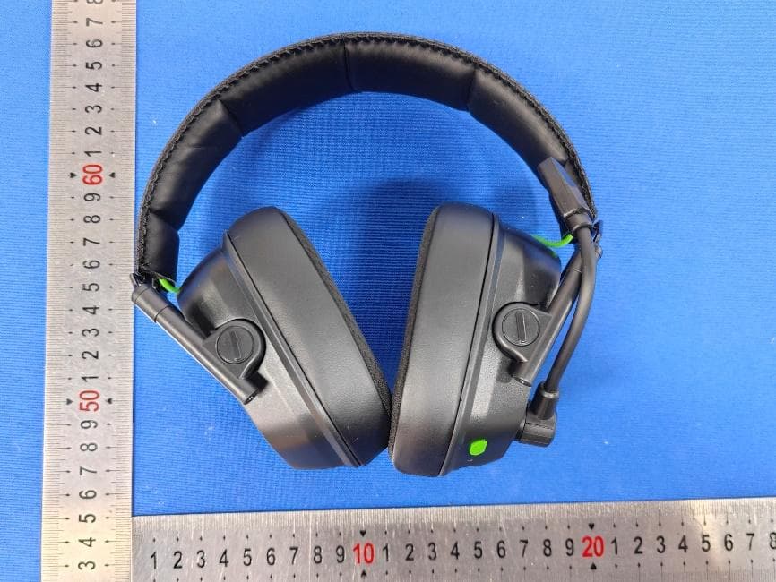
2BATE-VK81
Sep 22, 2025Wireless Gaming Headset
Equipment Class
DTS - Digital Transmission System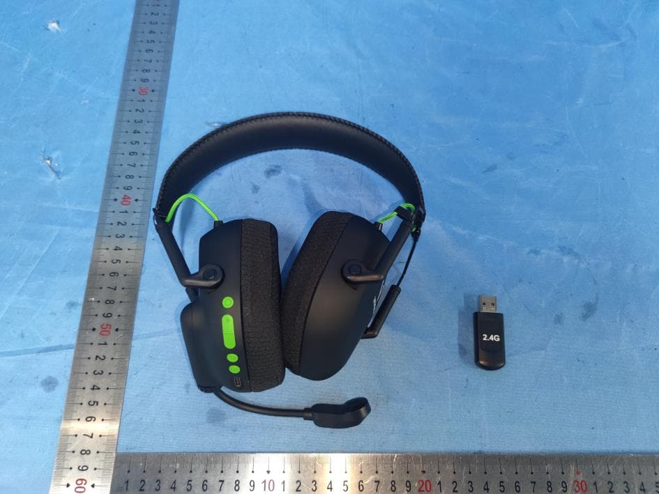
2BATE-HW20
Aug 03, 2024Wireless Gaming Headset
Equipment Class
DSS - Part 15 Spread Spectrum Transmitter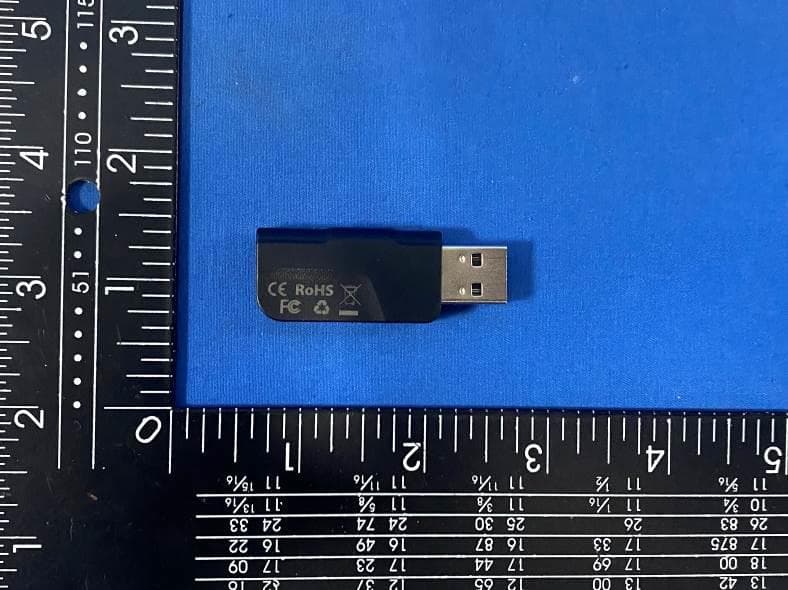
2BATE-WG1-1
Oct 06, 2023Wireless Gaming Headset
Equipment Class
DXX - Part 15 Low Power Communication Device Transmitter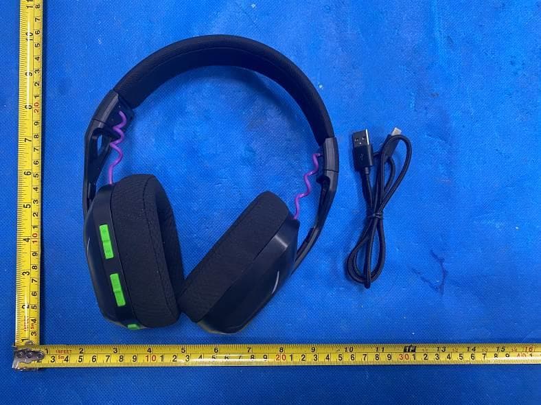
2BATE-WG1
Oct 06, 2023Wireless Gaming Headset
Equipment Class
DSS - Part 15 Spread Spectrum Transmitter