2BCMP-ASW14Camera
Ausek Limited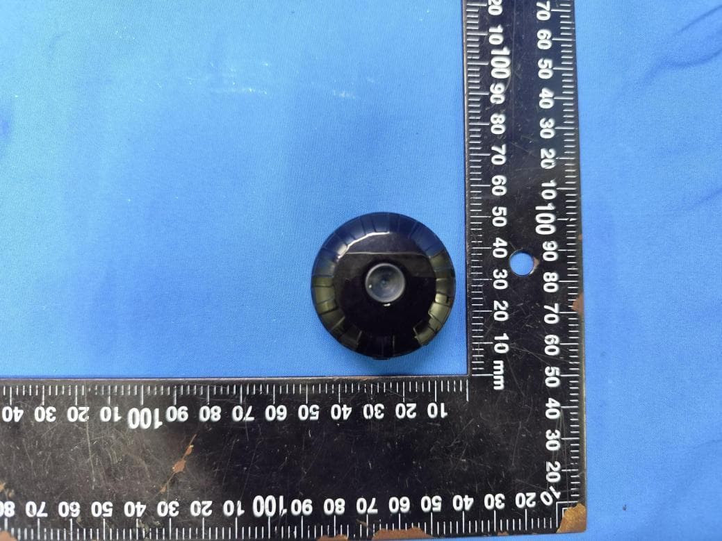
Click to zoom
Application Details
- Equipment Class
- DTS - Digital Transmission System
- Date of Grant
- Dec 10, 2025
- Application Purpose
- Original Equipment
- Equipment Note
- Camera
- Frequency Range
- 2412.00000000 - 2462.00000000
- Company
- Ausek Limited
- Country
- China
Documents & Files
Document Text
Text extracted from the exhibit documents filed with the FCC. Open a document above to read the original.
Users Manual
FCC Caution: This device complies with part 15 of the FCC Rules. Operation is subject to the following two conditions: (1) This device may not cause harmful interference, and (2) this device must accept any interference received, including interference that may cause undesired operation. Any changes or modifications not expressly approved by the party responsible for compliance could void the user's authority to operate the equipment. NOTE: This equipment has been tested and found to comply with the limits for a Class B digital device, pursuant to Part 15 of the FCC Rules. These limits are designed to provide reasonable protection against harmful interference in a residential installation. This equipment generates, uses and can radiate radio frequency energy and, if not installed and used in accordance with the instructions, may cause harmful interference to radio communications. However, there is no guarantee that interference will not occur in a particular installation. If this equipment does cause harmful interference to radio or television reception, which can be determined by turning the equipment off and on, the user is encouraged to try to correct the interference by one or more of the following measures: -- Reorient or relocate the receiving antenna. -- Increase the separation between the equipment and receiver. -- Connect the equipment into an outlet on a circuit different from that to which the receiver is connected. -- Consult the dealer or an experienced radio/TV technician for help. The device has been evaluated to meet general RF exposure requirement. The device can be used in portable exposure condition without restriction.
Attestation Statements
LocalRepresentativeLetter ForCertificationServiceintheUSA FederalCommunicationsCommission EquipmentAuthorizationDivision,ApplicationProcessingBranch 7435OaklandMillsRoad Columbia,MD21048 Towhomitmayconcern PursuanttoSection2.911(d)(7),oftheCommission’sRules(47C.F.R.)weattestasfollowsfor theproductlistedbelow: FCCIDModelname 2BCMP-ASW14AS-W14,AS-W9,AS-W9D,AS-W10,AS-W11, AS-W12,AS-W13,AS-W15,AS-W16,AS- W17,AS-W18,AS-W19,AS-W20 Weherebyacknowledgeasfollows: i.bothsigneesconfirmthatthepointofcontactacceptsresponsibilitytoactasaUS- AmericanRepresentativeonbehalfoftheapplicant ii.thepointofcontactprovidesthephysicalU.S.addressandemailaslistedbelow iii.bothpartiesmaintaintherequirementsofthisagreementwithoutexpirationdate US-AmericanPointofContactApplicant/ApprovalHolder SignatureSignature CompanyName:LOBOSIOWAINCAusekLimited FRN:00364139610034165829 ContactName:HarleyLiSarahTang Address:4623BittercreekDrColorado SpringsCO80922US No.4Building,JianjinBusiness Park,DonghuansecondRoad, LonghuaDistrict,Shenzhen, China Phone:+18188180538008613927439912 Email:[email protected]@ausek.com
Attestation Statements
CoveredEquipmentAttestationLetter ForCertificationServiceintheUSA FederalCommunicationsCommission EquipmentAuthorizationDivision,ApplicationProcessingBranch 7435OaklandMillsRoad Columbia,MD21048 Towhomitmayconcern PursuanttoSection2.911(d)(5)(i)-(ii)oftheCommission’sRules(47C.F.R.)weattestas followsfortheproductlistedbelow: FCCIDModelname 2BCMP-ASW14AS-W14,AS-W9,AS-W9D,AS-W10,AS- W11,AS-W12,AS-W13,AS-W15,AS-W16, AS-W17,AS-W18,AS-W19,AS-W20 We, Applicant CompanyName:AusekLimited Address:No.4Building,JianjinBusinessPark, DonghuansecondRoad,LonghuaDistrict, Shenzhen,China Phone:008613927439912 certifythattheequipmentforwhichauthorizationissoughtisnot“covered”equipment prohibitedfromreceivinganequipmentauthorizationpursuanttosection2.903oftheFCC rules.Thisincludesthecybersecurityandanti-virussoftwareproducedorprovidedby KasperskyLab,Inc.oranyofistsuccessorsandassignees. Wecertifythat,asofthedateofthefilingoftheapplication,theapplicantisnotidentified ontheCoveredListasanentityproducing“covered”equipment. Ifyouhaveanyquestions,pleasefeelfreetocontactusattheaddressshownbelow. Sincerely, 2025-12-4 SignatureDate PrintedNameofSignee:SarahTang Company:AusekLimited Phone:008613927439912 Email:[email protected] Address:No.4Building,JianjinBusinessPark, DonghuansecondRoad,LonghuaDistrict, Shenzhen,China Fax:N/A
Cover Letter(s)
AusekLimited No.4Building,JianjinBusinessPark,DonghuansecondRoad,LonghuaDistrict,Shenzh en,China Date:2025-12-4 FCCID:2BCMP-ASW14 ModelNumber:AS-W14,AS-W9,AS-W9D,AS-W10,AS-W11,AS-W12,AS-W13,, AS-W15,AS-W16,AS-W17,AS-W18,AS-W19,AS-W20 To:FederalCommunicationCommission AuthorizationandEvaluationDivision7435OaklandMillsRoad Columbia,MD21048 ToWhomItMayConcern, We,AusekLimitedherebydeclarethatourproduct(Camera ) ModelNumber: AS-W14, AS-W9,AS-W9D,AS-W10,AS-W11,AS-W12,AS-W13,,AS-W15,AS-W16,AS-W17, AS-W18,AS-W19,AS-W20 electricalidentical,theSchematic,PCBlayout,structureand softwarearesame,onlythedifferenceisthemodelnameandcolorformarketpurpose. Shouldyouhaveanyquestionsorcommentsregardingthismatter,pleasehave mybestattention. Sincerely, (Signed) Name/Title:SarahTang/Manager Company:AusekLimited Address:No.4Building,JianjinBusinessPark,DonghuansecondRoad,LonghuaDistrict, Shenzhen,China Phone:008613927439912 FaxNumber:N/A E-Mail:[email protected]
Cover Letter(s)
ConfidentialityRequestLetter ForCertificationServiceintheUSA FederalCommunicationCommission EquipmentAuthorizationDivision,ApplicationProcessingBranch 7435OaklandMillsRoad Columbia,MD21048 Towhomitmayconcern PursuanttoParagraphs§0.457and0.459oftheCommission’sRules(47C.F.R.)andSection §552(b)(4)oftheFreedomofInformationAct,werequestconfidentialityforthe documentationofthefollowingproducts: FCCIDModelname 2BCMP-ASW14AS-W14,AS-W9,AS-W9D,AS-W10,AS-W11, AS-W12,AS-W13,AS-W15,AS-W16,AS-W17, AS-W18,AS-W19,AS-W20 Fortheproductslistedabove,werequestpermanentconfidentialityforallapplicable exhibitsasthereare: theOperationalDescription theBlockDiagram theSchematics Theabovelistedexhibitscontaintradesecretsandproprietaryinformationthatcouldbeof benefittoourcompetitors. Ifyouhaveanyquestions,pleasefeelfreetocontactusattheaddressshownbelow. Sincerely, 2025-12-4 SignatureDate PrintedNameofSignee/Title:SarahTang/Manager Company:AusekLimited Address:No.4Building,JianjinBusinessPark,DonghuansecondRoad,LonghuaDistrict, Shenzhen,China Phone:008613927439912 Fax:N/A Email:[email protected]
External Photos
ReportNo.:CISRR250728212 Page 39 of 56 7.EXTERNALANDINTERNALPHOTOS 7.1.ExternalPhotos ReportNo.:CISRR250728212 Page 40 of 56 ReportNo.:CISRR250728212 Page 41 of 56
ID Label/Location Info
Label Size:10mm*10mm FCCID:2BCMP-ASW14 LabelLocation
Internal Photos
ReportNo.:CISRR250728212 Page 42 of 56 7.2.InternalPhotos ANT ReportNo.:CISRR250728212 Page 43 of 56
RF Exposure Info
RFExposureevaluation FCCID2BCMP-ASW14 ProductNameCamera ModelNo.AS-W14 ListedModel(s) AS-W9,AS-W9D,AS-W10,AS-W11,AS-W12,AS-W13, AS-W15,AS-W16,AS-W17,AS-W18,AS-W19,AS-W20 ExposurecategoryGeneralpopulation/uncontrolledenvironment EUTTypeProductionUnit DeviceTypePortableDevice 1.Reference ANSIC95.1–1999:IEEEStandardforSafetyLevelswithRespecttoHumanExposureto RadioFrequencyElectromagneticFields,3kHzto300GHz. FCCKDBpublication447498D01GeneralRFExposureGuidancev06:MobileandPortable DevicesRFExposureProceduresandEquipmentAuthorizationPolicies. FCCCFR47parBMK24041.1310:Radiofrequencyradiationexposurelimits. FCCCFR47part22.1093:Radiofrequencyradiationexposureevaluation:portabledevices 2.Requirement AccordingtoKDB447498D01GeneralRFExposureGuidancev06Section4.3.1Standalone SARtestexclusionconsiderations:“UnlessspecificallyrequiredbythepublishedRFexposure KDBprocedures,standalone1-gheadorbodyand10-gextremitySARevaluationforgeneral populationexposureconditions,bymeasurementornumericalsimulation,isnotrequired whenthecorrespondingSARTestExclusionThresholdcondition,listedbelow,issatisfied. Thesetestexclusionconditionsarebasedonsource-basedtime-averagedmaximum conductedoutputpoweroftheRFchannelrequiringevaluation,adjustedfortune-uptolerance, andtheminimumtestseparationdistancerequiredfortheexposureconditions.22The minimumtestseparationdistanceisdeterminedbythesmallestdistancefromtheantenna andradiatingstructuresoroutersurfaceofthedevice,accordingtothehostformfactor, exposureconditionsandplatformrequirements,toanypartofthebodyorextremityofauser orbystander(see5)ofsection4.1).ToqualifyforSARtestexclusion,thetestseparation distancesappliedmustbefullyexplainedandjustifiedbytheoperatingconfigurationsand exposureconditionsofthetransmitterandapplicablehostplatformrequirements,typicallyin theSARmeasurementorSARanalysisreport,accordingtotherequiredpublishedRF exposureKDBprocedures.WhennootherRFexposuretestingorreportingisrequired,a statementofjustificationandcompliancemustbeincludedintheequipmentapproval,inlieuof theSARreport,toqualifyfortheSARtestexclusion.Whenrequired,thedevicespecific conditionsdescribedintheotherpublishedRFexposureKDBproceduresmustbesatisfied beforeapplyingtheseSARtestexclusionprovisions;forexample,handheldPTTtwo-way radios,handsets,laptops&tabletsetc.23” [(max.powerofchannel,includingtune-uptolerance,mW)/(min.testseparationdistance, mm)]·[√f(GHz)]≤3.0for1-gSARand≤7.5for10-gextremitySAR,where: •f(GHz)istheRFchanneltransmitfrequencyinGHz •PoweranddistanceareroundedtothenearestmWandmmbeforecalculation •Theresultisroundedtoonedecimalplaceforcomparison •3.0and7.5arereferredtoasthenumericthresholdsinthestep2below Thetestexclusionsareapplicableonlywhentheminimumtestseparationdistanceis≤50mm andfortransmissionfrequenciesbetween100MHzand6GHz.Whentheminimumtest separationdistanceis<5mm,adistanceof5mmaccordingto5)insection4.1isappliedto determineSARtestexclusion. Whenoneofthefollowingtestexclusionconditionsissatisfiedforallcombinationsof simultaneoustransmissionconfigurations,furtherequipmentapprovalisnotrequiredto incorporatetransmittermodulesinhostdevicesthatoperateinthemixedmobileandportable hostplatformexposureconditions.Thegranteeisresponsiblefordocumentingthisaccording toClassIpermissivechangerequirements.AntennasthatqualifyforstandaloneSARtest exclusionmustapplytheestimatedstandaloneSARtodeterminesimultaneoustransmission testexclusion. a)The[∑of(thehighestmeasuredorestimatedSARforeachstandaloneantenna configuration,adjustedformaximumtune-uptolerance)/1.6W/kg]+[∑ofMPEratios]is≤ 1.0. b)TheSARtopeaklocationseparationratiosofallsimultaneouslytransmittingantennapairs operatinginportabledeviceexposureconditionsareall≤0.04,andthe[∑ofMPEratios]is≤ 1.0. 3.ConductedPeakOutputPower ModeChannel PeakOutputPower (dBm) PeakOutputPower (mW) IEEE802.11b 18.597.23 67.896.15 118.446.98 IEEE802.11g 18.396.90 67.896.15 118.226.64 IEEE802.11n_20 18.266.70 67.916.18 118.056.38 4.ManufacturingTolerance IEEE802.11b ChannelChannel1Channel6Channel11 Target(dBm)878 Tolerance±(dB)1.01.01.0 IEEE802.11g ChannelChannel1Channel6Channel11 Target(dBm)878 Tolerance±(dB)1.01.01.0 IEEE802.11n_20 ChannelChannel1Channel6Channel11 Target(dBm)878 Tolerance±(dB)1.01.01.0 5.EvaluationResult Band/Modef(GHz) Antenna Distance (mm) RFoutputpower SARTest Exclusion Threshold SARTest Exclusion dBmmW 11N(HT20)246259 7.94 2.4927<3.0Yes Remark: 1.Outputpowerincludingtuneuptolerance; 2.Whentheminimumtestseparationdistanceis<5mm,adistanceof5mmaccordingtof)in section4.1isappliedtodetermineSARtestexclusion. 6.Conclusion ThemeasurementresultscomplywiththeFCCLimitper47CFR2.1093fortheuncontrolled RFExposureandSARExclusionThresholdperKDB447498D01V06. ------Endofthereport------
Test Report
Application Note AN043 Small Size 2.4 GHz PCB antenna By Audun Andersen 1 KEYWORDS • CC25xx • CC24xx • CC2480 • PCB antenna • USB dongle • 2.4 GHz • Inverted F Antenna 2 INTRODUCTION The PCB antenna used on the CC2511 USB dongle reference design is described in this application note. Even if the antenna presented is for a USB dongle design it can be used in all 2.4 GHz designs, especially where small space is required for the antenna. This application note describes the antenna dimensions, the RF performance and considerations for complying with regulatory limits when using this design. The suggested antenna design requires no more than 15.2 x 5.7 mm of space and ensures a VSWR ratio of less than 2 across the 2.4 GHz ISM band when connected to a 50 ohm source. Figure 1: CC2511 USB Dongle SWRA117D Page 1 of 21 Application Note AN043 Table of Contents 1 KEYWORDS...................................................................................................................1 2 INTRODUCTION.............................................................................................................1 3 ABBREVIATIONS...........................................................................................................2 4 ANTENNA DESIGN........................................................................................................3 4.1 DESIGN GOALS..........................................................................................................3 4.2 SIMULATION...............................................................................................................3 4.3 LAYOUT AND IMPLEMENTATION...................................................................................4 5 TEST RESULTS.............................................................................................................5 5.1 REFLECTION..............................................................................................................5 5.2 RADIATION PATTERN..................................................................................................7 5.3 OUTPUT POWER......................................................................................................15 5.4 SPURIOUS EMISSION AND HARMONICS......................................................................17 6 CONCLUSION ..............................................................................................................20 7 GENERAL INFORMATION..........................................................................................21 7.1 DOCUMENT HISTORY................................................................................................21 3 ABBREVIATIONS CAD Computer Aided Design CC24xx CC2400, CC2420, CC2430 and CC2431 CC25xx CC2500, CC2510, CC2511, CC2550 and CC2520 CC2480 Z-Accel ZigBee Processor IFA Inverted F Antenna ISM Industrial, Scientific and Medical LOS Line Of Sight PCB Printed Circuit Board PER Packet Error Rate VSWR Voltage Standing Wave Ratio SWRA117D Page 2 of 21 Application Note AN043 4 ANTENNA DESIGN The PCB antenna on the CC2511 USB dongle reference design is a meandered Inverted F Antenna (IFA). The IFA was designed to match an impedance of 50 ohm at 2.45 GHz. Thus no additional matching components are necessary. 4.1 Design Goals The reflection at the feed point of the antenna determines how much of the applied power is delivered to the antenna. A reflection of less than -10 dB across the 2.4 GHz ISM band, when connected to a 50 ohm source, was a design goal. Reflection of less than -10 dB, or VSWR less than 2, ensures that more than 90% of the available power is delivered to the antenna. Bandwidth is in this document defined as the frequency band where more than 90% of the available power is delivered to the antenna. Another design goal was to fit the size of the PCB antenna on a USB dongle and to obtain good performance also when the dongle is connected to a computer. 4.2 Simulation IE3D from Zeland, which is an electromagnetic simulation tool, was used to design the antenna. The accuracy of the simulation is controlled by the mesh. An increase of the mesh increases the simulation time. Thus, for initial simulations mesh = 1 should be used. When a fairly good result is achieved a higher mesh should be used to obtain more accurate results. Comparison of simulation and measurement results shows that the measured reflection is between the result obtained with mesh = 5 and mesh = 1; see Figure 2 for details. Figure 2: Comparison of Simulation and Measurements Results SWRA117D Page 3 of 21 Application Note AN043 4.3 Layout and Implementation Small changes of the antenna dimensions may have large impact on the performance. Therefore it is strongly recommended to make an exact copy of the reference design to achieve optimum performance. The easiest way to implement the antenna is to import the gerber or DXF file showing the antenna layout. These files are named IFA_USB.spl and IFA_USB.dxf respectively and are included in the CC2511 USB dongle reference design available from http://www.ti.com\lpw. The imported file can be used as a template when drawing the antenna. By using this procedure it should be possible to make an exact copy. If the PCB CAD tool being used does not support import of DXF or gerber files, Figure 3 and Table 1 should be used to ensure correct implementation. It is recommended to generate a gerber file for comparison with IFA_USB.spl when making a manual implementation. Most gerber viewers have the possibility to import several gerber files at the same time. Thus by placing the gerber file, showing the manually implemented antenna, on top of IFA_USB.spl it is easy to verify that the antenna is correctly implemented. It is also recommended to use the same thickness and type of PCB material as used in the reference design. Information about the PCB can be found in a separate readme file included in the reference design. To compensate for a thicker/thinner P…
Text truncated - open the document above for the full version.
Test Report
ReportNo.:CISRR250728212 Thetestresultsrelateonlytothetestedsamples. ThetestreportshouldnotbereproducedexceptinfullwithoutthewrittenapprovalofShenzhenBangce TestingTechnologyCo.,Ltd. Page1of48 TESTREPORT ReportNo.CISRR250728212 ProjectNo.CISR250728212 FCCID2BCMP-ASW14 ApplicantAusekLimited Address No.4Building,JianjinBusinessPark,DonghuansecondRoad,Longhua District,Shenzhen,China ManufacturerAusekLimited Address No.4Building,JianjinBusinessPark,DonghuansecondRoad,Longhua District,Shenzhen,China ProductNameCamera TradeMarkN/A Model/TypereferenceAS-W14 ListedModel(s) AS-W9,AS-W9D,AS-W10,AS-W11,AS-W12,AS-W13,AS-W15, AS-W16,AS-W17,AS-W18,AS-W19,AS-W20 Standard 47CFRPart15.247 TestdateJuly28,2025toAugust1,2025 IssuedateAugust5,2025 TestresultComplied Preparedby:JimmyHuangApprovedby:GenryLong ReportNo.:CISRR250728212 Page 2 of 48 Contents 1.REPORTVERSION..........................................................................................................................................3 2.TESTDESCRIPTION.......................................................................................................................................4 3.SUMMARY........................................................................................................................................................5 3.1.ProductDescription*..................................................................................................................................5 3.2.RadioSpecificationDescription*..............................................................................................................5 3.3.ModificationofEUT.....................................................................................................................................5 3.4.Deviationfromstandards...........................................................................................................................6 3.5.TestingSite...................................................................................................................................................6 4.TESTCONFIGURATION.................................................................................................................................7 4.1.Testfrequencylist.......................................................................................................................................7 4.2.Descriptionsoftestmode...........................................................................................................................7 4.3.Supportunitusedintestconfiguration....................................................................................................7 4.4.Testsampleinformation.............................................................................................................................7 4.5.Environmentalconditions...........................................................................................................................7 4.6.Statementofthemeasurementuncertainty.............................................................................................8 4.7.EquipmentUsedduringtheTest................................................................................................................8 5.TESTRESULTS.............................................................................................................................................10 5.1.EvaluationResults(Evaluation)...............................................................................................................10 5.1.1.AntennaRequirement............................................................................................................................10 5.2.RadioSpectrumMatterTestResults(RF)...............................................................................................11 5.2.1.ConductedEmissionatACpowerline.................................................................................................11 5.2.2.6dBBandwidth........................................................................................................................................14 5.2.3.MaximumConductedOutputPower.....................................................................................................15 5.2.4.PowerSpectralDensity..........................................................................................................................16 5.2.5.Conductedbandedgeandspuriousemission...................................................................................17 5.2.6.Radiatedbandedgeemission...............................................................................................................18 5.2.7.RadiatedSpuriousEmission(below1GHz).........................................................................................24 5.2.8.RadiatedSpuriousEmission(Above1GHz)........................................................................................28 6.APPENDIXREPORT......................................................................................................................................36 6.1.DutyCycle..................................................................................................................................................36 6.2.PowerSpectralDensity.............................................................................................................................38 6.3.ConductedOutputPower.........................................................................................................................40 6.4.6dBBandwidth...........................................................................................................................................42 6.5.ConductedOutOfBandEmission...........................................................................................................44 ReportNo.:CISRR250728212 Page 3 of 48 1.REPORTVERSION VersionNo.IssuedateDescription 00August5,2025Original…
Text truncated - open the document above for the full version.
Test Setup Photos
ReportNo.:CISRR250728212 Page 37 of 56 6.TESTSETUPPHOTOS ConductedEmissionatACpowerline Radiatedbandedgeemission RadiatedSpuriousEmission(Above1GHz) ReportNo.:CISRR250728212 Page 38 of 56 RadiatedSpuriousEmission(below1GHz)
Contact Information
Applicant
Sarah Tang
[email protected]Fax: 0755-86165667
Test Firm
Shenzhen Bangce Testing Technology Co. , Ltd.Hans Hu
Technical Specifications
| # | Rule Parts | Frequency Range | Power Output |
|---|---|---|---|
| 1 | 15C | 2.41 GHz - 2.46 GHz | 7.23 mW |
Other Applications from Ausek Limited
2BCMP-ASB101
Jul 15, 2026Mini wifi camera
Equipment Class
DTS - Digital Transmission System
2BCMP-AX07
Jul 14, 2026WIFI REPEATER
Equipment Class
NII - Unlicensed National Information Infrastructure TX
2BCMP-AX10
Jul 14, 2026WIFI REPEATER
Equipment Class
NII - Unlicensed National Information Infrastructure TX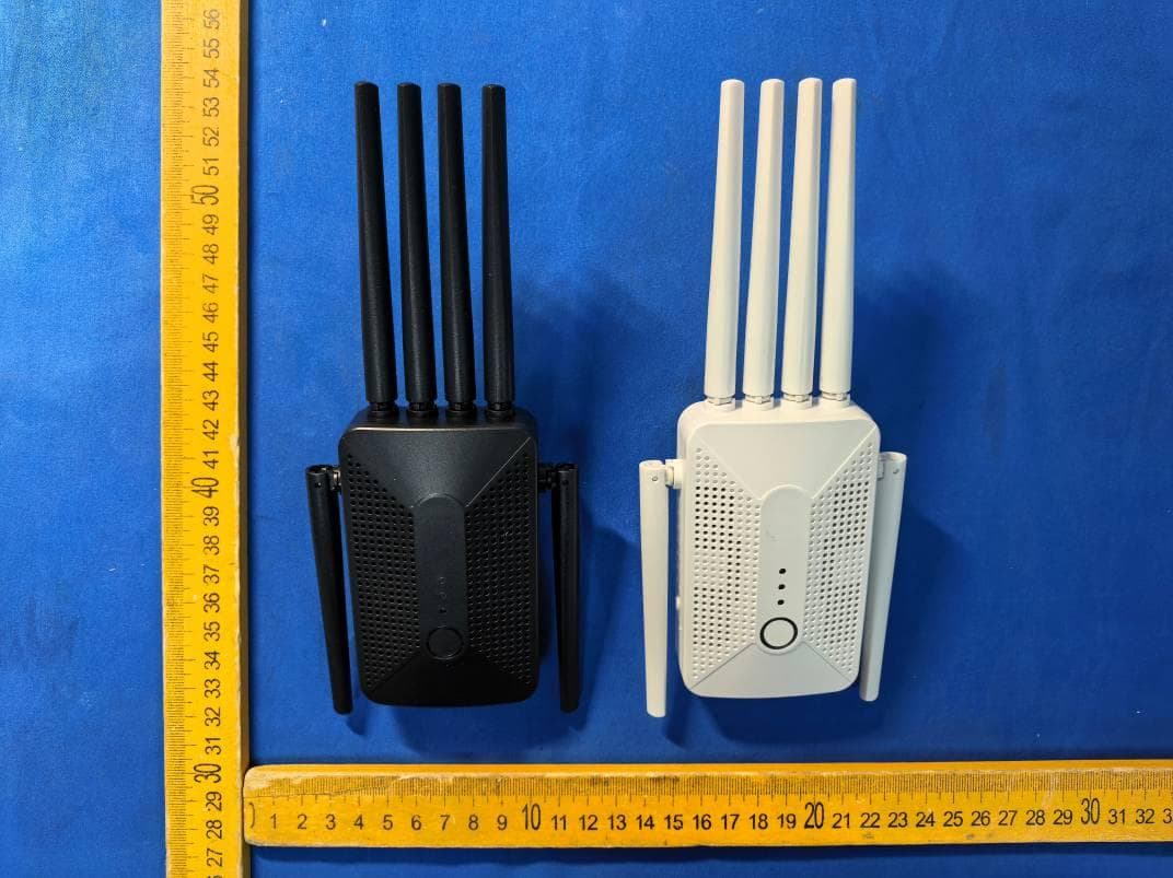
2BCMP-97B
Jul 14, 2026WIFI REPEATER
Equipment Class
DTS - Digital Transmission System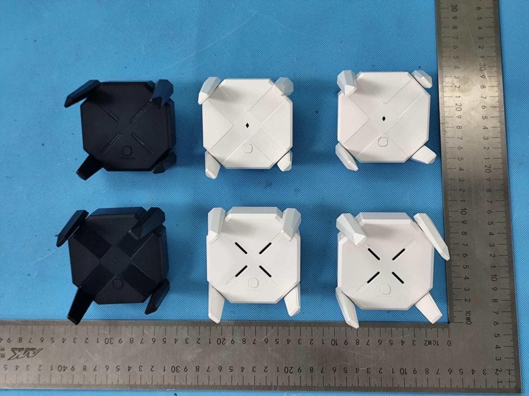
2BCMP-A18
Jun 11, 2026Repeater
Equipment Class
DTS - Digital Transmission System