2BCVO-BHD-TW6Wireless earphone
Guangdong Pisen Electronics Co., Ltd.
Click to zoom
Application Details
- Equipment Class
- DTS - Digital Transmission System
- Date of Grant
- Feb 04, 2024
- Application Purpose
- Original Equipment
- Date of Application
- Feb 04, 2024
- Equipment Note
- Wireless earphone
- Frequency Range
- 2402.00000000 - 2480.00000000
- Country
- China
Documents & Files
Document Text
Text extracted from the exhibit documents filed with the FCC. Open a document above to read the original.
Attestation Statements
Guangdong Pisen Electronics Co., Ltd. * the applicant must designate a contact located in the United States for purposes of acting as the applicant’s agent for service of process, regardless of whether the applicant is a domestic or foreign entity. An applicant located in the United States may designate itself as the agent for service of process. U.S. Agent Designation for Service of Process - Certification Attestation Letter 1/12/2024 Nemko North America, Inc. 303 River Road Ottawa K1V 1H2 Canada ATTN.: Reviewing Engineer FCC ID: 2BCVO-BHD-TW6 Per section 2.911(d)(7) of the FCC rules, Guangdong Pisen Electronics Co., Ltd. (“the applicant”) certifies that the equipment for which authorization is sought is designated to the following U.S. agent* for service of process: Federal Registration Number (FRN): 0033402884 Company Name: FCC US Agent, LLC Physical U.S. Company Address: 3722 Illinois Avenue, Saint Charles, IL, 60174, USA Agent name: Tim Payne Agent Email Address: [email protected] The above contact person accepts the obligation for service of process. The applicant accepts to maintain an agent for no less than one year after the grantee has terminated all marketing and importation or the conclusion of any Commission-related proceeding involving the equipment. Applicants Federal Registration Number (FRN): 0034240226 Company Name: Guangdong Pisen Electronics Co., Ltd. Company Address: No.9, Qinfu 1st Street, Jintang Industry Zone, Niushipu Village, Liuyue, Henggang Town, Longgang District, Shenzhen City, Guangdong Province, PEOPLE'S REPUBLIC OF CHINA Agent name: Zhang Zhang Agent Email Address: [email protected] Applicant Signed: Agent Signed (if different to Applicant): Signed: Signed: Printed name: Zhang Zhang Printed name:Tim Payne Title: Supervisor Title: Manager Company Name: Guangdong Pisen Electronics Co., Ltd. Company Name: FCC US Agent, LLC Date: 1/12/2024 Date: 1/12/2024
Attestation Statements
Guangdong Pisen Electronics Co., Ltd. Covered Equipment Certification Attestation Letter DATE Nemko North America, Inc. 303 River Road Ottawa K1V 1H2 Canada ATTN.: Reviewing Engineer FCC ID: 2BCVO-BHD-TW6 Guangdong Pisen Electronics Co., Ltd. (“the applicant”) certifies that the equipment for which authorization is sought is not “covered” equipment prohibited from receiving an equipment authorization pursuant to section 2.903 of the FCC rules. Note: If the equipment for which the applicant seeks authorization is produced by any of the entities identified on the current Covered List, the applicant should include an explanation on why the equipment is not “covered” equipment. Guangdong Pisen Electronics Co., Ltd. (“the applicant”) certifies that, as of the date of the filing of the application, the applicant is not identified on the Covered List as an entity producing “covered” equipment. Signed: Printed name: Zhang Zhang Title: Supervisor Company Name: Guangdong Pisen Electronics Co., Ltd Date: 1/12/2024
Cover Letter(s)
Guangdong Pisen Electronics Co., Ltd. Date: 2024.01.12 Equipment Autorisation Division Federal Communications Commission 7435 Oakland Mills Road Columbia, MD 21046 FCC ID: 2BCVO-BHD-TW6 Product Name: Wireless earphone Request for Confidentiality Pursuant to Sections 0.457 and 0.459 of the commissions rules, we hereby request that the following documents be held confidential: • Schematics • Block Diagram • Operation Description These materials contain trade secrets and proprietary information and are not customarily released to the public. The public disclosure of this information might be harmful to the company and provide unjustified benefits to our competitors. Signature: Name: Zhang Zhang Company: Guangdong Pisen Electronics Co., Ltd. Address: No.9, Qinfu 1st Street, Jintang Industry Zone, Niushipu Village, Liuyue, Henggang Town, Longgang District, Shenzhen City, Guangdong Province, PEOPLE'S REPUBLIC OF CHINA Phone: 0755-28508800-8860 Fax: / Email: [email protected]
Cover Letter(s)
Guangdong Pisen Electronics Co., Ltd. Equipment Autorisation Division Federal Communications Commission 7435 Oakland Mills Road Columbia, MD 21046 Date: 2024.01.12 SUBJECT: FCC Application for FCC ID: 2BCVO-BHD-TW6 To Whom It May Concern: We, the undersigned, hereby authorize _ Walter Chen _ at _CTC Laboratories, Inc. on our behalf, to apply to the Federal Communications Commission on our equipment. Any and all acts carried out by _ Walter Chen _ on our behalf shall have the same effect as acts of our own. This is to advise that we are in full compliance with the Anti- Drug Abuse Act. We, the applicant, are not subject to a denial of federal benefits pursuant to Section 5301 of the Anti-Drug Act of 1988, 21 USC853a, and no party to the application is subject to a denial of federal benefits pursuant to that section. Regards, Signature: Name: Zhang Zhang Company: Guangdong Pisen Electronics Co., Ltd. Address: No.9, Qinfu 1st Street, Jintang Industry Zone, Niushipu Village, Liuyue, Henggang Town, Longgang District, Shenzhen City, Guangdong Province, PEOPLE'S REPUBLIC OF CHINA Phone: 0755-28508800-8860 Fax: / Email: [email protected]
External Photos
CTC Laboratories, Inc. 1-2/F., Building 2, Jiaquan Building, Guanlan High-Tech Park, Shenzhen, Guangdong, China Tel: +86-755-27521059 Fax: +86-755-27521011 http://www.sz-ctc.org.cn Page 1 of 7 External Photographs Page 2 of 7 Report No.: CTC20232378E Page 2 of 7 Page 3 of 7 Report No.: CTC20232378E Page 3 of 7 Page 4 of 7 Report No.: CTC20232378E Page 4 of 7 Page 5 of 7 Report No.: CTC20232378E Page 5 of 7 Page 6 of 7 Report No.: CTC20232378E Page 6 of 7 Page 7 of 7 Report No.: CTC20232378E Page 7 of 7
ID Label/Location Info
CTC Laboratories, Inc. 2/F., Building 1 and 1-2/F., Building 2, Jiaquan Building, Guanlan High-Tech Park, Longhua District, Shenzhen, Guangdong, China Tel: +86-755- 27521059 Fax: +86-755- 27521011 Http://www.sz-ctc.org.cn Page 1 of 1 Label and Label Location 1.
Internal Photos
CTC Laboratories, Inc. 1-2/F., Building 2, Jiaquan Building, Guanlan High-Tech Park, Shenzhen, Guangdong, China Tel: +86-755-27521059 Fax: +86-755-27521011 http://www.sz-ctc.org.cn Page 1 of 5 Internal Photographs Page 2 of 5 Report No.: CTC20232378E Page 2 of 5 Page 3 of 5 Report No.: CTC20232378E Page 3 of 5 Page 4 of 5 Report No.: CTC20232378E Page 4 of 5 Page 5 of 5 Report No.: CTC20232378E Page 5 of 5 ANT
RF Exposure Info
CTC Laboratories, Inc. 1-2/F., Building 2, Jiaquan Building, Guanlan High-Tech Park, Shenzhen, Guangdong, China Tel: +86-755-27521059 Fax: +86-755-27521011 http://www.sz-ctc.com.cn CTC Laboratories, Inc. 1-2/F., Building 2, Jiaquan Building, Guanlan High-Tech Park, Shenzhen, Guangdong, China Tel.: (86)755-27521059 Fax: (86)755-27521011 Http://www.sz-ctc.org.cn For anti-fake verification, please visit the official website of Certification and Accreditation Administration of the People’s Republic of China : http://yz.cnca.cn RF Exposure Evaluation FCC ID: 2BCVO-BHD-TW6 According to KDB447498 D01 General RF Exposure Guidance v06, Clause 4.3.1(a) EUT Specification EUT Wireless earphone Trade Mark: PISEN Model/Type reference: BHD-TW6 Listed Model(s): / Frequency band (Operating) BT: 2.402GHz ~ 2.480GHz Device category Portable (<5mm separation) Mobile (>20cm separation) Fixed (>20cm separation) Others ___ Antenna diversity Single antenna Multiple antennas Tx diversity Rx diversity Tx/Rx diversity Antenna gain (Max) 2.58dBi Limit For 100 MHz to 6 GHz and test separation distances ≤ 50 mm, the 1-g and 10-g SAR test exclusion thresholds are determined by the following: [(max. power of channel, including tune-up tolerance, mW) / (min. test separation distance, mm)] · [√f (GHz) ] ≤ 3.0 for 1-g SAR, and ≤ 7.5 for 10-g extremity SAR Where -f (GHz) is the RF channel transmit frequency in GHz -Power and distance are rounded to the nearest mW and mm before calculation -The result is rounded to one decimal place for comparison -The values 3.0 and 7.5 are referred to as numeric thresholds in step b) below The test exclusions are applicable only when the minimum test separation distance is ≤ 50 mm, and for transmission frequencies between 100 MHz and 6 GHz. When the minimum test separation distance is < 5 mm, a distance of 5 mm according to 4.1 f) is applied to determine SAR test exclusion. Page 2 of 2 Report No.: CTC20232378E03 CTC Laboratories, Inc. 1-2/F., Building 2, Jiaquan Building, Guanlan High-Tech Park, Shenzhen, Guangdong, China Tel.: (86)755-27521059 Fax: (86)755-27521011 Http://www.sz-ctc.org.cn For anti-fake verification, please visit the official website of Certification and Accreditation Administration of the People’s Republic of China : http://yz.cnca.cn Measurement Result Mode Channel Frequency (MHz) Max. Measured Power (dBm) Max. Tune up Power (dBm) Result Limit GFSK (BLE 2M) 2402 -3.72 -3 0.281 3.0 GFSK (EDR) 2441 0.98 1 0.713 3.0 Note: 1. Calculate by Worst-case mode. 2. Max. Tune Up Power by Manufacturer's Declaration, and Max. Tune Up Power is used to calculate. 3. For a more detailed features description, please refer to the RF Test Report. **********************THE END**********************
Test Report
CTC Laboratories, Inc. 2/F., Building 1 and 1-2/F., Building 2, Jiaquan Building, Guanlan High-Tech Park, Longhua District, Shenzhen, Guangdong, China Tel: +86-755-27521059 Fax: +86-755-27521011 Http://www.sz-ctc.org.cn TEST REPORT Report No. .................................... : CTC20232378E01 FCC ID ........................................... : 2BCVO-BHD-TW6 Applicant ...................................... : Guangdong Pisen Electronics Co., Ltd. Address .......................................... : No.9, Qinfu 1st Street, Jintang Industry Zone, Niushipu Village, Liuyue, Henggang Town, Longgang District, Shenzhen City, Guangdong Province, PEOPLE'S REPUBLIC OF CHINA Manufacturer..................................: Guangdong Pisen Electronics Co., Ltd. Address..........................................: No.9, Qinfu 1st Street, Jintang Industry Zone, Niushipu Village, Liuyue, Henggang Town, Longgang District, Shenzhen City, Guangdong Province, PEOPLE'S REPUBLIC OF CHINA Product Name .............................. : Wireless earphone Trade Mark .................................... : PISEN Model/Type reference .................... : BHD-TW6 Listed Model(s) .............................. : / Standard ....................................... : FCC CFR Title 47 Part 15 Subpart C Section 15.247 Date of receipt of test sample........: Dec. 25, 2023 Date of testing..............................: Dec. 27, 2023 ~ Jan. 8, 2024 Date of issue................................: Jan. 19, 2024 Result............................................: PASS Compiled by: (Printed name+signature) Lucy Lan Supervised by: (Printed name+signature) Eric Zhang Approved by: (Printed name+signature) Totti Zhao $英文检测章$ $Totti$ Testing Laboratory Name ........... : CTC Laboratories, Inc. Address .......................................... : 2/F., Building 1 and 1-2/F., Building 2, Jiaquan Building, Guanlan High-Tech Park, Longhua District, Shenzhen, Guangdong, China This test report may be duplicated completely for legal use with the approval of the applicant. It should not be reproduced except in full, without the written approval of our laboratory. The client should not use it to claim product endorsement by CTC. The Test Result in the report only apply to the tested sample. The test report shall be invalid without all the signatures of testing engineers, reviewer and approver. Any objections must be raised to CTC within 15 days since the date when the report is received. It will not be taken into consideration beyond this limit. The test report merely corresponds to the test sample. Page 2 of 57 Report No.: CTC20232378E01 CTC Laboratories, Inc. 2/F., Building 1 and 1-2/F., Building 2, Jiaquan Building, Guanlan High-Tech Park, Longhua District, Shenzhen, Guangdong, China Tel.: (86)755-27521059 Fax: (86)755-27521011 Http://www.sz-ctc.org.cn For anti-fake verification, please visit the official website of Certification and Accreditation Administration of the People’s Republic of China : http://yz.cnca.cn Table of Contents Page 1. TEST SUMMARY ....................................................................................................................................................... 3 1.1. TEST STANDARDS .................................................................................................................................................. 3 1.2. REPORT VERSION .................................................................................................................................................. 3 1.3. TEST DESCRIPTION ................................................................................................................................................. 3 1.4. TEST FACILITY ....................................................................................................................................................... 4 1.5. MEASUREMENT UNCERTAINTY .................................................................................................................................. 5 1.6. ENVIRONMENTAL CONDITIONS ................................................................................................................................. 5 2. GENERAL INFORMATION .......................................................................................................................................... 6 2.1. CLIENT INFORMATION............................................................................................................................................. 6 2.2. GENERAL DESCRIPTION OF EUT ................................................................................................................................ 6 2.3. ACCESSORY EQUIPMENT INFORMATION....................................................................................................................... 7 2.4. OPERATION STATE ................................................................................................................................................. 8 2.5. MEASUREMENT INSTRUMENTS LIST ........................................................................................................................... 9 3. TEST ITEM AND RESULTS ........................................................................................................................................ 10 3.1. CONDUCTED EMISSION ......................................................................................................................................... 10 3.2. RADIATED EMISSION ............................................................................................................................................ 13 3.3. BAND EDGE EMISSIONS (RADIATED) ........................................................................................................................ 24 3.4. BAND EDGE AND SPURIOUS EMISSIONS (CONDUCTED) .................................................................................................…
Text truncated - open the document above for the full version.
Test Report
2.4GHz 2012 Chip Antenna:YL2012F1P2G45 __________________________________________________________________________________ Application: WLAN, 802.11b/g, Bluetooth, etc... Features SMD, high reliability, ultra Impact, Omni-directional... Part number 2012 - F0 YL (1) (2) (3) P 2G45 (4) (5) (1)Product Type Chip Antenna (2)Size Code 2.0x1.2mm (3)Type Code F1 (4)Packing Paper Tape (5)Frequency 2.45GHz Electrical Specification W orking Frequency Range 2400 ~2484 MHz Peak Gain 2.58dBi (Typ.) Impedance 50 Ohm Return loss 10 dB ( Min) Polarization Linear Azimuth Beamwidth Omni-directional Operation Temperature(°C) -40 ~85°C The specification is defined on EVB. Dimension and Terminal Configuration 永联无线 2.4GHz 2012 Chip Antenna: YL2012F1P2G45 Electrical Characteristics Return Loss & Radiation Return Loss Frequency (MHz) (dB) 200010 209223.5 215510 Radiation Return Loss ______________________________________________________________________________________________________ Evaluation Board Reference PCB Dimension Antenna Layout Reference Unit :mm Unit :mm 2.4GHz 2012 Chip Antenna: YL2012F1P2G45 ______________________________________________________________________________________________________ Taping Specifications Reel and Taping Specification Reel Specification Tapping Specification TYPE SIZE A ψB ψC ψD W ψM 2012 7” 5K/Reel 2.0±0.5 13.5±1.0 21±1.0 60±1.0 11.5±2.0 178±2.0 Packaging Type A B W E F G H T ψD P Paper Type 20121.90±0.20 3.50±0.20 8.0±0.20 1.75±0.10 3.5±0.05 4.0±0.10 2.0±0.05 0.75±0.10 +0.10 1.50 -0 4.0±0.1 2.4GHz 2012 Chip Antenna: YL2012F1P2G45 ______________________________________________________________________________________________________ Reliability Table Test ItemProcedure Requirements Ceramic Type Remark (Reference) Electrical Characterization Fulfill the electrical specification User Spec. Thermal Shock 1. Preconditioning: 50 ± 10°C / 1 hr , then keep for 24 ± 1 hrs at room temp. 2. Initial measure: Spec: refer Initial spec. 3. Rapid change of temperature test: -30°C to +85°C; 100 cycles; 15 minutes at Lower category temperature; 15 minutes at Upper category temperature. No Visible Damage. Fulfill the electrical specification. MIL-STD-202 107 Temperature Cycling 1. Initial measure: Spec: refer Initial spec. 2. 100 Cycles (-30°C to +85°C), Soak Mode=1 (2 Cycle/hours). 3. Measurement at 24 ± 2Hours after test condition. No Visible Damage. Fulfill the electrical specification. JESD22 JA104 High Temperature Exposure 1. Initial measure: Spec: refer Initial spec. 2. Unpowered; 500hours @ T=+85°C. 3. Measurement at 24 ± 2 hours after test. No Visible Damage. Fulfill the electrical specification. MIL-STD-202 108 Low Temperature Storage 1. Initial measure: Spec: refer Initial spec. 2. Unpowered: 500hours @ T= -30°C. 3. Measurement at 24 ± 2 hours after test. No Visible Damage. Fulfill the electrical specification. MIL-STD-202 108 Solderability (SMD Bottom Side) Dipping method: a. Temperature: 235 ± 5°C b. Dipping time: 3 ± 0.5s The solder should cover over 95% of the critical area of bottom side. IEC 60384-21/22 4.10 Soldering Heat Resistance (RSH) Preheating temperature: 150 ± 10°C. Preheating time: 1~2 min. Solder temperature: 260 ± 5°C. Dipping time: 5 ± 0.5s No Visible Damage.IEC 60384-21/22 4.10 Vibration5g's for 20 min., 12 cycles each of 3 orientations Note: Use 8"X5" PCB .031" thick 7 secure points on, one long side and 2 secure points at corners of opposite sides. Parts mounted within 2" from any secure point. Test from 10-2000 Hz. No Visible Damage.MIL-STD-202 Method 204 Mechanical Shock Three shocks in each direction shall be applied along the three mutually perpendicular axes of the test specimen (18 shocks) Peak value: 1,500g’s Duration: 0.5ms Velocity change: 15.4 ft/s Waveform: Half-sine No Visible Damage.MIL-STD-202 Method 213 Humidity Bias 1. Humidity: 85% R.H., Temperature: 85 ± 2 °C. 2. Time: 500 ± 24 hours. 3. Measurement at 24 ± 2hrs after test condition. No Visible Damage. Fulfill the electrical specification. MIL-STD-202 Method 106 2.4GHz 2012 Chip Antenna: YL2012F1P2G45 ______________________________________________________________________________________________________ Revision History Revision Date Content 1 2022/1/20New issue Board Flex (SMD) 1. Mounting method: IR-Reflow. PCB Size (L:100 × W:40 × T:1.6mm) 2. Apply the load in direction of the arrow until bending reaches 2 mm. No Visible Damage.AEC-Q200 005 AdhesionForce of 1.8Kg for 60 seconds.No Visible Damage Magnification of 20X or greater may be employed for inspection of the mechanical integrity of the device body terminals and body/terminal junction. AEC-Q200 006 Physical Dimension Any applicable method using x10 magnification, micrometers, calipers, gauges, contour projectors, or other measuring equipment, capable of determining the actual specimen dimensions. In accordance with specification. JESD22 JB100 Manufacturer: ShenZhen City Flink Wi Technology CO.,LTD. Address: 606 Huachuangda Business Building, Yu'an 1st Road, Bao'an 45 District, Shenzhen
Test Report
2.4GHz 2012 Chip Antenna:YL2012F1P2G45 __________________________________________________________________________________ Application: WLAN, 802.11b/g, Bluetooth, etc... Features SMD, high reliability, ultra Impact, Omni-directional... Part number 2012 - F0 YL (1) (2) (3) P 2G45 (4) (5) (1)Product Type Chip Antenna (2)Size Code 2.0x1.2mm (3)Type Code F1 (4)Packing Paper Tape (5)Frequency 2.45GHz Electrical Specification W orking Frequency Range 2400 ~2484 MHz Peak Gain 2.58dBi (Typ.) Impedance 50 Ohm Return loss 10 dB ( Min) Polarization Linear Azimuth Beamwidth Omni-directional Operation Temperature(°C) -40 ~85°C The specification is defined on EVB. Dimension and Terminal Configuration 永联无线 2.4GHz 2012 Chip Antenna: YL2012F1P2G45 Electrical Characteristics Return Loss & Radiation Return Loss Frequency (MHz) (dB) 200010 209223.5 215510 Radiation Return Loss ______________________________________________________________________________________________________ Evaluation Board Reference PCB Dimension Antenna Layout Reference Unit :mm Unit :mm 2.4GHz 2012 Chip Antenna: YL2012F1P2G45 ______________________________________________________________________________________________________ Taping Specifications Reel and Taping Specification Reel Specification Tapping Specification TYPE SIZE A ψB ψC ψD W ψM 2012 7” 5K/Reel 2.0±0.5 13.5±1.0 21±1.0 60±1.0 11.5±2.0 178±2.0 Packaging Type A B W E F G H T ψD P Paper Type 20121.90±0.20 3.50±0.20 8.0±0.20 1.75±0.10 3.5±0.05 4.0±0.10 2.0±0.05 0.75±0.10 +0.10 1.50 -0 4.0±0.1 2.4GHz 2012 Chip Antenna: YL2012F1P2G45 ______________________________________________________________________________________________________ Reliability Table Test ItemProcedure Requirements Ceramic Type Remark (Reference) Electrical Characterization Fulfill the electrical specification User Spec. Thermal Shock 1. Preconditioning: 50 ± 10°C / 1 hr , then keep for 24 ± 1 hrs at room temp. 2. Initial measure: Spec: refer Initial spec. 3. Rapid change of temperature test: -30°C to +85°C; 100 cycles; 15 minutes at Lower category temperature; 15 minutes at Upper category temperature. No Visible Damage. Fulfill the electrical specification. MIL-STD-202 107 Temperature Cycling 1. Initial measure: Spec: refer Initial spec. 2. 100 Cycles (-30°C to +85°C), Soak Mode=1 (2 Cycle/hours). 3. Measurement at 24 ± 2Hours after test condition. No Visible Damage. Fulfill the electrical specification. JESD22 JA104 High Temperature Exposure 1. Initial measure: Spec: refer Initial spec. 2. Unpowered; 500hours @ T=+85°C. 3. Measurement at 24 ± 2 hours after test. No Visible Damage. Fulfill the electrical specification. MIL-STD-202 108 Low Temperature Storage 1. Initial measure: Spec: refer Initial spec. 2. Unpowered: 500hours @ T= -30°C. 3. Measurement at 24 ± 2 hours after test. No Visible Damage. Fulfill the electrical specification. MIL-STD-202 108 Solderability (SMD Bottom Side) Dipping method: a. Temperature: 235 ± 5°C b. Dipping time: 3 ± 0.5s The solder should cover over 95% of the critical area of bottom side. IEC 60384-21/22 4.10 Soldering Heat Resistance (RSH) Preheating temperature: 150 ± 10°C. Preheating time: 1~2 min. Solder temperature: 260 ± 5°C. Dipping time: 5 ± 0.5s No Visible Damage.IEC 60384-21/22 4.10 Vibration5g's for 20 min., 12 cycles each of 3 orientations Note: Use 8"X5" PCB .031" thick 7 secure points on, one long side and 2 secure points at corners of opposite sides. Parts mounted within 2" from any secure point. Test from 10-2000 Hz. No Visible Damage.MIL-STD-202 Method 204 Mechanical Shock Three shocks in each direction shall be applied along the three mutually perpendicular axes of the test specimen (18 shocks) Peak value: 1,500g’s Duration: 0.5ms Velocity change: 15.4 ft/s Waveform: Half-sine No Visible Damage.MIL-STD-202 Method 213 Humidity Bias 1. Humidity: 85% R.H., Temperature: 85 ± 2 °C. 2. Time: 500 ± 24 hours. 3. Measurement at 24 ± 2hrs after test condition. No Visible Damage. Fulfill the electrical specification. MIL-STD-202 Method 106 2.4GHz 2012 Chip Antenna: YL2012F1P2G45 ______________________________________________________________________________________________________ Revision History Revision Date Content 1 2022/1/20New issue Board Flex (SMD) 1. Mounting method: IR-Reflow. PCB Size (L:100 × W:40 × T:1.6mm) 2. Apply the load in direction of the arrow until bending reaches 2 mm. No Visible Damage.AEC-Q200 005 AdhesionForce of 1.8Kg for 60 seconds.No Visible Damage Magnification of 20X or greater may be employed for inspection of the mechanical integrity of the device body terminals and body/terminal junction. AEC-Q200 006 Physical Dimension Any applicable method using x10 magnification, micrometers, calipers, gauges, contour projectors, or other measuring equipment, capable of determining the actual specimen dimensions. In accordance with specification. JESD22 JB100 Manufacturer: ShenZhen City Flink Wi Technology CO.,LTD. Address: 606 Huachuangda Business Building, Yu'an 1st Road, Bao'an 45 District, Shenzhen
Test Setup Photos
CTC Laboratories, Inc. 1-2/F., Building 2, Jiaquan Building, Guanlan High-Tech Park, Shenzhen, Guangdong, China Tel: +86-755- 27521059 Fax: +86-755- 27521011 Http://www.sz-ctc.org.cn Page 1 of 2 Radiated Measurements Below 1GHz Above1GHz Page 2 of 2 Report No.: CTC20232378E Page 2 of 2 Conducted Emissions
Contact Information
Applicant
Zhang Zhang
Test Firm
CTC Laboratories, Inc.Totti Zhao
[email protected]+8675527521059
Technical Specifications
| # | Rule Parts | Frequency Range | Power Output |
|---|---|---|---|
| 1 | 15C | 2.40 GHz - 2.48 GHz | 1.25 mW |
Other Applications from Guangdong Pisen Electronics Co., Ltd.
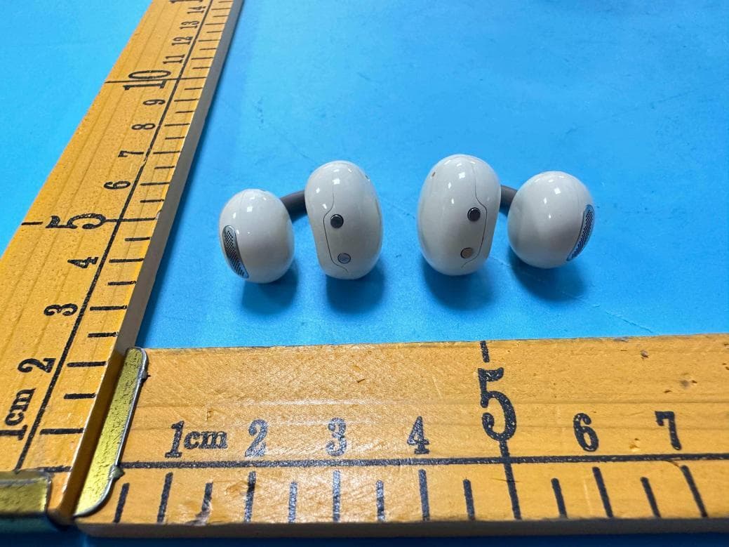
2BCVO-EHB-TW2
Dec 18, 2025PISEN CloudFeather Open Ear Clip-On Earbuds
Equipment Class
DSS - Part 15 Spread Spectrum Transmitter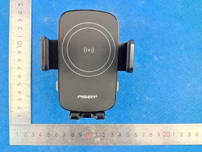
2BCVO-TP-C69
Aug 29, 2024Pisen 15W Wireless Auto Clamping Car Mount Charger
Equipment Class
DCD - Part 15 Low Power Transmitter Below 1705 kHz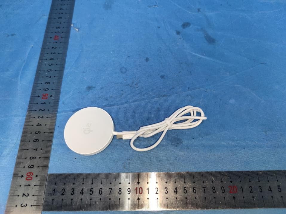
2BCVO-TP-C74
Aug 27, 2024PISEN-Qi2 Magnetic Desktop Charging Base(Lite)
Equipment Class
DCD - Part 15 Low Power Transmitter Below 1705 kHz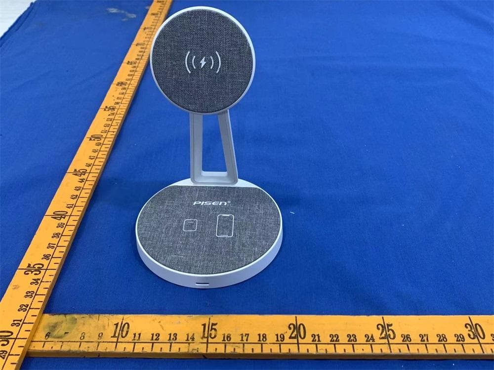
2BCVOTP-C30
Jun 19, 2024PISEN - 2-in-1 Night Light Wireless Charging Stand
Equipment Class
DCD - Part 15 Low Power Transmitter Below 1705 kHz
2BCVO-BHD-TW14
Apr 09, 2024Wireless earphone
Equipment Class
DTS - Digital Transmission System