A2DA2T179GGSM MOBILE PHONE-GSM PORTION
Shenzhen Telacom Science & Technology Co., Ltd.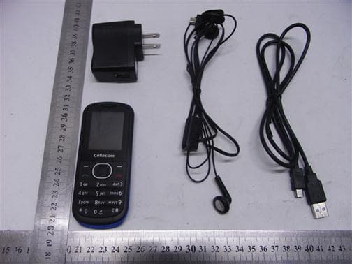
Click to zoom
Application Details
- Equipment Class
- PCE - PCS Licensed Transmitter held to ear
- Date of Grant
- Dec 07, 2011
- Application Purpose
- Original Equipment
- Date of Application
- Dec 07, 2011
- Equipment Note
- GSM MOBILE PHONE-GSM PORTION
- Frequency Range
- 1850.20000000 - 1909.80000000
- Country
- China
Documents & Files
Document Text
Text extracted from the exhibit documents filed with the FCC. Open a document above to read the original.
Users Manual
T179 User manual www.cellacom.com2 Contents 1 About your Mobile Phone.............................. 7 1.1Appearance..............................................7 1.2Key instructions...................................... 8 1.3Icons........................................................10 2 Getting started..................................................10 2.1The Battery............................................10 2.1.1 Install&remove a battery ...... 11 2.1.2 Charging ...................................... 11 2.2SIM card installation............................12 2.3Memory card installation.................... 13 2.4Storage Management.......................... 14 2.5Power on and off.................................14 3 Call functions....................................................15 3.1Makeacall........................................... 15 3.1.1 Make a domestic call ............... 15 3.1.2 Make an extension call ........... 15 3.1.3 Make an international call ....... 16 3.1.4 Make a call from Mobile Phone book16 3.1.5 Redial a call by recent call lists 16 3.2Answer a call........................................16 3.3Reject a call..........................................17 3.4Call options............................................17 4 Menu functions................................................ 17 4.1Messages............................................... 17 www.cellacom.com3 4.1.1 Write message ........................... 17 4.1.2 Inbox ............................................. 18 4.1.3 Outbox .......................................... 18 4.1.4 Settings ........................................ 18 4.1.5 Memory Status ........................... 19 4.1.6 Voice mail ................................... 19 4.1.7 Broadcast Message .................. 19 4.2Multimedia.............................................. 20 4.2.1 FM Radio .................................... 20 4.2.2 Audio player ................................ 20 4.3Organizer................................................21 4.3.1 Calendar ...................................... 21 4.3.2 To do list ..................................... 21 4.3.3 Alarm ............................................ 21 4.3.4 Calculator ..................................... 22 4.4Settings...................................................22 4.4.1 Time and Date ........................... 22 4.4.2 Display ......................................... 22 4.4.3 Phone setting ............................. 22 4.4.4 Call settings ................................ 23 4.4.5 Network Setting .......................... 25 4.4.6 Network status ........................... 25 4.4.7 Security Setup ............................ 25 4.4.8 Set UART .................................... 26 4.4.9 Restore Factory settings .......... 26 4.5File Manager......................................... 27 4.6Phonebook............................................. 27 www.cellacom.com4 4.6.1 Contacts ....................................... 27 4.6.2 Add new contact ....................... 28 4.6.3 Delete ALL .................................. 28 4.6.4 Copy All ....................................... 28 4.6.5 Owner number ........................... 29 4.6.6 Preferred Storage ...................... 29 4.6.7 Memory Status ........................... 29 4.6.8 Speed dial ................................... 29 4.7Call history.............................................29 4.8Fun&Game.........................................30 5 Battery information......................................... 30 6 Safety information........................................... 31 6.1Operating environment........................31 6.2Electronic devices................................ 31 6.2.1 Pacemaker .................................. 31 6.2.2 Hearing aids ............................... 32 6.2.3 Other medical devices ............. 32 6.2.4 Vehicles ....................................... 33 6.3Potentially dangerous situations....... 33 7 Care and maintenance...................................33 www.cellacom.com5 Preface Thank you very much for your choice of this product designed by our company ! Our Mobile Phone complies with the Telecommunication industries standards of both the People ' s Republic of China and Europe . The product described in this guide is approved for use on the GSM networks,and has the GPRS functions. GSM network is a global cellular communications system of international standards . Allow you to receive an international telephone call used as in your homeland . However , before using these advanced network functions , you must firstly apply for these required services . In order to better use your mobile phone , we suggest you to carefully read this statement to know all the functions well. Note : Due to the cellular network settings and the services provided , some functions may be unavailable , please query local service providers. For your safety Read these simple guidelines . Breaking the rules may be dangerous or illegal . Further detailed information is given in www.cellacom.com6 this manual. ROAD SAFETY Always keep your hands free to operate the vehicle while driving . Park the vehicle before using your Mobile Phone . SWITCH OFF IN AIRCRAFT Using of wireless telephones in aircraft may disrupt the operation of the aircraft . It is dangerous and illegal . Insure switching off the Mobile Phone before going aboard. SWITCH OFF IN HOSPITALS Follow any restrictions or rules . Switch off the Mobile Phone near medical equipment . SWITCH OFF WHEN REFUELING Switch off the Mobile Phone at a refueling point or any fuel or chemicals places . SWITCH OFF NEAR BLASTING POINT Don ’ t use the Mobile Phone where blasting is in progress . Observe restrictions , and follow any regulations or rules . INTERFERENCE All wireless Mobile Phones may be susceptible to interference,which could affect the performance. USE NORMALLY Use in the normal position explained in the product documentation . Don ' t touch…
Text truncated - open the document above for the full version.
Block Diagram
ANT RF T/R 26MHZ VCTCXO MT6252 RDA6221 RF PA+Switch SIM1 SIM2 Receiver MIC Speaker LCD Keypad 32.768kHz crystal
External Photos
FCC ID: A2DA2T179GReport No.: MOST111104F1 FRONT VIEW OF SAMPLE BACK VIEW OF SAMPLE FCC ID: A2DA2T179GReport No.: MOST111104F1 LEFT VIEW OF SAMPLE RIGHT VIEW OF SAMPLE FCC ID: A2DA2T179GReport No.: MOST111104F1 TOP VIEW OF SAMPLE BOTTOM VIEW OF SAMPLE FCC ID: A2DA2T179GReport No.: MOST111104F1 PHOTO OF EARPHONE PHOTO OF USB CABLE FCC ID: A2DA2T179GReport No.: MOST111104F1 PHOTO OF POWER SUPPLY PHOTO OF BATTERY FCC ID: A2DA2T179GReport No.: MOST111104F1 PHOTO OF THE ENTIRE SAMPLE
Internal Photos
FCC ID: A2DA2T179GReport No.: MOST111104F1 INTERNAL PHOTO OF SAMPLE – 1 INTERNAL PHOTO OF SAMPLE – 2 FCC ID: A2DA2T179GReport No.: MOST111104F1 INTERNAL PHOTO OF SAMPLE –3 INTERNAL PHOTO OF SAMPLE –4 FCC ID: A2DA2T179GReport No.: MOST111104F1 INTERNAL PHOTO OF POWER SUPPLY-1 INTERNAL PHOTO OF POWER SUPPLY-2
Operational Description
1/2 Operation Description OPERATIONAL DESCRIPTION APPLICANT:Shenzhen Telacom Science & Technology Co., Ltd Manufacturer: FINMEK ELECTRONIC (SHENZHEN) CO., LTD FCC ID: A2DA2T179G Instruction Book: Users Manual Frequency Range GSM Transmit Frequency Band: 824.2-848.8 MHz Receive Frequency Band: 849.2-893.8 MHz Transmit Frequency Band: 1850.2-1909.8 MHz Receive Frequency Band: 1930.2-1989.8 MHz Specific Operating Power Range: Power Class 1; Power Control Level 0 +30dBm +2.0dB/-2.0dB Power Control Level 1 +28dBm +3.0dB/-3.0dB Power Control Level 2 +26dBm +3.0dB/-3.0dB Power Control Level 3 +24dBm +3.0dB/-3.0dB Power Control Level 4 +22dBm +3.0dB/-3.0dB Power Control Level 5 +20dBm +3.0dB/-3.0dB Power Control Level 6 +18dBm +3.0dB/-3.0dB Power Control Level 7 +16dBm +3.0dB/-3.0dB Power Control Level 8 +14dBm +3.0dB/-3.0dB Power Control Level 9 +12dBm +4.0dB/-4.0dB Power Control Level 10 +10dBm +4.0dB/-4.0dB Power Control Level 11 +8dBm +4.0dB/-4.0dB Power Control Level 12 +6dBm +4.0dB/-4.0dB Power Control Level 13 +4dBm +4.0dB/-4.0dB Power Control Level 14 +2dBm +5.0dB/-5.0dB Power Control Level 15 +0dBm +5.0dB/-5.0dB Note; Effective radiation efficiency is –3.7dB DC Voltage and Current into the Final Amplifier Module: Supply Voltage = 5.0Vdc Supply Current = ~0.5Amp. Tune-up Procedure: Tune-up Procedure Equipment Identification: Equipment's Identification label and its intended Location are as shown in EXHIBIT Type “ID Label / Location Information” (FCC ID Nameplate), and in EXHIBIT Type “Internal Photo”(Photograph of inside) Photographs: A complete set of the Photographs showing External and Internal Views of Circuit Details and Construction are provided by from EXHIBIT Type “External Photos” and “Internal Photos”. Accessories: Accessories 2/2 Operation Description Figure 1.2: Terminal Components (Accessories) Technical Descriptions TX synthesizer uses an Offset-PLL circuit. The Offset-PLL circuit consists of PLL-IC and TX_VCO and loop filter. Reference frequency of the above synthesizers is 26MHz and generated by VCTCXO. Control signal is sent from Baseband section and keeps frequency stability. TX IQ signal is input from Baseband section to MT6252, The FM signal is input form TLG1120 section to MT6252. TX IQ signal is applied to the quadrature up-converter, and the up-converter LO signal is generated from the transceiver VCO . This up-converter translates the GMSK-modulated signal to an intermediate frequency (IF) that forms one input to a frequency/phase detector circuit. This IF signal is the reference input to an Offset-PLL circuit. The feedback path of this Offset-PLL circuit includes a down-conversion from the RF output frequency range to the IF range. The two inputs to this down-conversion mixer are formed the TX_VCO output and the LO generation circuits. The mixer output is the offset feedback signal that forms the variable input to a frequency/phase detector circuit. The detector compares its variable input to its reference input and generates an error signal that is low-pass filtered by the loop filter and applied to TX_VCO to force the RF frequency in the direction that minimizes errors. The TX_VCO output passes PA, Antenna SW, Coaxial connector with switch and emitted from embedded antenna. Digital Modulation: Analog speech produced by a microphone is encoded to digital PCM samples using a CODEC. The PCM samples are passed to a Vocoder for AMR (Advanced Multi Rate) encoding, to compress the speech samples. The encoding rate is determined by the Vocoder which formats the speech samples as data packets. A new data packet with data rate information is read by the microprocessor every 20 ms. The speech CODEC becomes AMR, FR(Full Rate), EFR(Enhanced FR) and HR(Half Rate). The microprocessor then sends the data packet to the transmit subsystem, and passed DAC to covert analog signal. I/Q base band signal is filtered and is inputted into 6M4003 containing quadrature phase modulator. Battery AC Charger
Parts List/Tune Up Info
项目 料号 描述 器件位置 用量 值 供应商名称 Item Part NO. Description Location QTY Value Supplier Name 1 K1752_4MBA_P0 PCBA 1 2 K1752_4MB_P0 PCB 1 麦德 3 C1005C0G1H2R2CT cap,2.2p,+/-0.25p,50V,C0G,0402 C187 C188 2 2.2pF TDK 4 C1005C0G1H3R9CT cap,3.9p,+/-0.25p,50V,C0G,0402 C185 C186 2 3.9pF TDK 5 C1005C0G1H050CT cap,5.0p,+/-0.5p,50V,C0G,0402 C191 C192 2 5.0pF TDK 6 C1005C0G1H5R6CT cap,5.6p,+/-0.25p,50V,C0G,0402 C168 1 5.6pF TDK 7 C1005C0G1H6R8CT cap,6.8p,+/-0.25p,50V,C0G,0402 C108 1 6.8pF TDK 8 C1005C0G1H080DT cap,8p,+/-0.5p,50V,C0G,0402 C189 C190 2 8.0pF TDK 9 C1005C0G1H180JT cap,18p,+/-5%,50V,C0G,0402 C162 C169 C193 C194 4 18pF TDK 10 C1005C0G1H220JT cap,22p,+/-5%,50V,C0G,0402 C101 C104 C105 C107 C109 C110 C111 C116 C117 C182 C184 11 22pF TDK 11 C1005C0G1H330JT cap,33p,+/-5%,50V,C0G,0402 C130 C131 C132 C133 C134 C135 C158 C159 8 33pF TDK 12 C1005C0G1H560JT cap,56p,+/-5%,50V,C0G,0402 C195 1 56pF TDK 13 C1005C0G1H101JT cap,100p,+/-5%,50V,C0G,0402 C140 C145 C152 C157 4 100pF TDK 14 C1005X7R1H221KT cap,220p,+/-5%,50V,C0G,0402 C106 1 220pF TDK 互 前线物料清单 15 C1005X7R1H102KT cap,1n,+/-10%,50V,X7R,0402 C123 C126 2 1nF TDK 16 C1005X7R1E103KT cap,10n,+/-10%,10V,X5R,0402 C102 1 10nF TDK 17 CC0402KRX5R6BB104 cap,100n,+/-10%,10V,X5R,0402 C141 C144 C146 C129 C154 C155 6 100nF YAGEO 18 C1005X5R0J105KT cap,1u,+/-10%,16V,X5R,0603 C121 C166 C167 C160 C161 C171C118 C124 C137 C163 C172 C173C175 C178 C179 C180 C197 C120C122 C127 C128 C136 C142 C148 C156 25 1uF 0402 TDK 19 C1608X5R0J225KT cap,2.2u,+/-10%,6.3V,X5R,0603 C176 C177 C196 3 2.2uF TDK 20 C1608X5R0J475KT cap,4.7u,+/-10%,6.3V,X5R,0603 C174 C164 2 4.7uF TDK 21 C2012X5R0J106K0J5N cap,10u,+/-20%,6.3V,0805,H=1.0mm C165 C181 C149 C150 C103 5 10uF 0805 TDK 22 RC0402JR-070RL res,0,+/-1%,0402 0.0625W C170 R113 R141 R142 R143 R144 L105 R140 R150 R151 R123 11 0R Yageo 23 RL0805FR-7W0R2L res,0.2R +/-5% 0.25W 0805 R137 1 0.2R 1% Yageo 24 RC0402JR-074R7L res,4.7R,+/-5%,0402 0.0625W R133 R134 2 4.7R Yageo 25 RC0402JR-0712RL res,12R,+/-5%,0402 0.0625W R111 R118 2 12R Yageo 26 RC0402JR-0733RL res,33R,+/-5%,0402 0.0625W R119 1 33R Yageo 27 RC0402JR-07220RL res,220R,+/-5%,0402 0.0625W R106 R109 R110 3 220R Yageo 28 RC0402JR-07270RL res,270,+/-5%,0402 0.0625W R128 R129 2 270R Yageo 29 RC0402JR-071KL res,1k,+/-5%,0402 0.0625W R101 R102 R104 R136 R139 R146R105 R124 R126 R116 R130 R132 12 1K Yageo 30 RC0402JR-071K5L res,1.5k,+/-5%,0402 0.0625W R125 R127 R131 3 1.5K Yageo 31 RC0402JR-074K7L res 4.7k,+/-5%,0402 0.0625W R107 R108 2 4.7K Yageo 32 RC0402JR-077K5L res,7.5K,+/-5%,0402 0.0625W R149 1 7.5K Yageo 33 RC0402JR-0710KL res,10k,+/-5%,0402 0.0625W R135 1 10K Yageo 34 RC0402JR-0724KL res,24k,+/-5%,0402 0.0625W R138 1 24K Yageo 35 RC0402JR-0730KL res,30k,+/-5%,0402 0.0625W R103 1 30K Yageo 36 RC0402JR-0739KL res,39k,+/-5%,0402 0.0625W R148 1 39K Yageo 37 RC0402JR-0747KL res,47k,+/-5%,0402 0.0625W R120 R121 R122 R115 4 47K Yageo 38 RC0402JR-07100KL res,100k,+/-5%,0402 0.0625W R145 R114 2 100K Yageo 39 RC0402JR-07300KL res,300k,+/-5%,0402 0.0625W R147 1 300K Yageo 40 MGCI1005T3N0ST-LF Chip Inductor,3.0nH,+/-0.3nH,Q>8,0402 L117 1 3.0nH Microgate 41 MGCI1005T3N3ST-LF Chip Inductor,3.3nH,+/-0. 3nH,Q>8,0402 L114 L115 L116 3 3.3nH Microgate 42 MGCI1005T3N9ST-LF Chip Inductor,3.9nH,+/-0. 3nH,Q>8,0402 L111 L112 2 3.9nH 0402 Microgate 43 MGCI1005T10NJT-LF Chip Inductor,10nH,+/-5%,Q>8,0402 L107 1 10nH Microgate 44 MGCI1005T18NJT-LF Chip Inductor,18nH,+/- 5%,Q>8,0402 L109 L110 2 18nH Microgate 45 MGCI1005T22NJT-LF Chip Inductor,22nH,+/-5%,Q>8,0402 L113 1 22nH Microgate 46 GZ2012D152 Z=1500ohm I=500mA L102 L103 2 GZ2012D152 Sunlord 47 MGGB1005M102HT-LF Ferrite bead,impendance=1000Ohm, 0402 B101 B102 B103 B104 B105 5 MGGB1005M102HT-LF Microgate 48 VRS0402SR55R330N Chip Varistor for Protecting against ESD D108 C138 C139 C143 C147 C151C153 D103 D104 D105 D106 D107 D110 13 VRS0402SR55R330N Chipcera 49 VRS0402KR090500N 9V Chip Varistor for Protecting against ESD D102 1 VRS0402KR090500N Chipcera 50 DTC123JMT2L NPN Bias Resistor Transistor Q101 1 DTC123JMT2L ROHM 51 PZ5D4V2H Ziner Diode 5.1v D109 1 PZ5D4V2H Prisemi 52 PT236T30E2 Hight gain low voltage PNP power transistor Q102 1 PT236T30E2 Prisemi 53 PNM723T703E0-2 N-Channel MOS Q103 1 PNM723T703E0-2 Prisemi 54 SGM3167YC6/TR SPDT Analog Switch in 6-pin SC70 U103 U104 2 SGM3167 SGMC 55 GT-197 ( 接受等级 X1.Q1) WHITE LED D101 D112 D113 D114 D115 D116 6 GT-197 Everlight 56 AOT-3806PW21B-N10-Y-3AA-M White LED 侧发光 D111 1 O T-3806PW21B-N10-Y-3A A AOT 57 X3S026000B71HZ-HPR TCVCXO 26MHz X101 1 26MHz HELE 58 SSP-T7-F(12.5pf,±20ppm) Crystal 32.768K U106 1 32.768K SII 59 EFCH881MTDA1 881.5 MHz SAW Filter U107 1 EFCH881MTDA1 Panasonic 60 EFCH9418TDL6 1842.5/942.5 MHz SAW Filter U108 1 EFCH9418TDL6 Panasonic 61 EFCH1960TDA1 1960 MHz SAW Filter U109 1 EFCH1960TDA1 Panasonic 62 RDA5802NM FM IC U102 1 RDA5802NM RDA 63 RDA6222 RF PA for GSM/EDGE 四频 U101 1 RDA6222 RDA 64 MT6252D BB IC U105 1 MT6252D MTK 65 03-2421138 TWO SIM +TF CARD J102 1 03-2421138 信为 66 KIU90531M1R 5PIN MICRO USB CONNECTOR CON101 1 KIU90531M1R KEIRAKU 67 BT038-53126F4252 battery connector,3pin CON102 1 BT038-53126F4252 弘宇微 68 K1752-BB-SHD sheding SHD101 1 K1752-BB-SHD Telacom 192
Parts List/Tune Up Info
!"#$% &'% % ('$)*+*)%,'$-./*#0%123$-%4.#0$5% 6(789:%;.#<5% %%%%%%%%%%%%%%%123$-%=>.??%@A% %%%%%%%%%%%%%%%123$-%=2#/2->%B$C$>%9%%%%%%%%DEE<;F%D:GE<;HI:GE<;% 123$-%=2#/2->%B$C$>%J%%%%%%%%DE@<;F%DKG:<;HIKG:<;% 123$-%=2#/2->%B$C$>%L%%%%%%%%DKM<;F%DKG:<;HIKG:<;% 123$-%=2#/2->%B$C$>%8%%%%%%%%DKL<;F%DKG:<;HIKG:<;% 123$-%=2#/2->%B$C$>%M%%%%%%%%DK9<;F%DKG:<;HIKG:<;% 123$-%=2#/2->%B$C$>%@:%%%%%%%DKE<;F%DKG:<;HIKG:<;% 123$-%=2#/2->%B$C$>%@@%%%%%%%DK@<;F%DKG:<;HIKG:<;% 123$-%=2#/2->%B$C$>%@K%%%%%%%D@M<;F%DKG:<;HIKG:<;% 123$-%=2#/2->%B$C$>%@E%%%%%%%D@L<;F%DKG:<;HIKG:<;% 123$-%=2#/2->%B$C$>%@N%%%%%%%D@9<;F%DKG:<;HIKG:<;% 123$-%=2#/2->%B$C$>%@9%%%%%%%D@E<;F%DKG:<;HIKG:<;% 123$-%=2#/2->%B$C$>%@J%%%%%%%D@@<;F%DKG:<;HIKG:<;% 123$-%=2#/2->%B$C$>%@L%%%%%%%DM<;F%DKG:<;HIKG:<;% 123$-%=2#/2->%B$C$>%@8%%%%%%%DL<;F%DKG:<;HIKG:<;% 123$-%=2#/2->%B$C$>%@M%%%%%%%D9<;F%DKG:<;HIKG:<;% 6(7@M::%;.#<5% 123$-%=>.??%@A% 123$-%=2#/-2>%B$C$>%:%%DE:<;F%DKG:<;HIKG:<;% 123$-%=2#/-2>%B$C$>%@%%DK8<;F%DEG:<;HIEG:<;% 123$-%=2#/-2>%B$C$>%K%%DKJ<;F%DEG:<;HIEG:<;% 123$-%=2#/-2>%B$C$>%E%%DKN<;F%DEG:<;HIEG:<;% 123$-%=2#/-2>%B$C$>%N%%DKK<;F%DEG:<;HIEG:<;% 123$-%=2#/-2>%B$C$>%9%%DK:<;F%DEG:<;HIEG:<;% 123$-%=2#/-2>%B$C$>%J%%D@8<;F%DEG:<;HIEG:<;% 123$-%=2#/-2>%B$C$>%L%%D@J<;F%DEG:<;HIEG:<;% 123$-%=2#/-2>%B$C$>%8%%D@N<;F%DEG:<;HIEG:<;% 123$-%=2#/-2>%B$C$>%M%%D@K<;F%DNG:<;HING:<;% 123$-%=2#/-2>%B$C$>%@:%%D@:<;F%DNG:<;HING:<;% 123$-%=2#/-2>%B$C$>%@@%%D8<;F%DNG:<;HING:<;% 123$-%=2#/-2>%B$C$>%@K%%DJ<;F%DNG:<;HING:<;% 123$-%=2#/-2>%B$C$>%@E%%DN<;F%DNG:<;HING:<;% 123$-%=2#/-2>%B$C$>%@N%%DK<;F%D9G:<;HI9G:<;% 123$-%=2#/-2>%B$C$>%@9%%D:<;F%D9G:<;HI9G:<;% % O2/$A%P++$)/*C$%-.<*./*2#%$++*)*$#)Q%*?%REGL<;% 1 Adjustment of RF Output Power: (1) The equipment setup as shown in Figure 1. (2) Operation of PC adjusts equipment. (3) Use RF Engineering Tools at PC side. Select GSM850 Band: 1) Set GSM850 Band. 2) Set ARFCN: 190 3) TX ON. 4) Adjust the power to 32.4dBm (+1.0dB/-1.0dB, Power control level: PCL=5) by PA DAC value. 5) Repeat 4) for 15 times,and adjust the power level to 30.5, 28.8, 27, 25, 23, 21, 19, 17, 15, 13, 11, 9, 7, 5. 6) Make 16 Ramp-Up/Ramp-Down data from the adjustment value of (5) and (6). PC RF Tester GPIB Cable UART Cable RF Cable Test sample Figure 1 7) Data of 5) and 6) is writen to flash memory. Select PCS1900 Band: 1) Set PCS Band. 2) Set ARFCN: 661. 3) TX ON. 4) Adjust the power to 29.0 dBm (+2.0dB/-2.0dB, Power control level: PCL=0) by PA DAC value. 5) Repeat 4) for 15 times,and adjust the power level to 27.5, 26, 24, 22, 20, 18, 16, 14, 12, 10, 8, 6, 4, 2, 0. 6) Make 16 Ramp-Up/Ramp-Down data from the adjustment value of (5) and (6). 7) Data of 5) and 6) is writen to flash memory. 2 Adjustment of oscillation frequency of VCXO: (1) The equipment setup as shown in Figure 1. (2) Use Crystal AFC Control Tools to Set CapID and AFC DAC value. (3) Set Band=GSM850,Set ARFCN=190,Set PCL=12. 1) Set AFC DAC=4096,fixed.(Check that Vafc=1.4V). 2) Set CapID=0, and verify that frequency error >>10KHz. 3) Set CapID=63, and verify that frequency error <<-10KHz. 4) If the above 3 items are verified, then change CapID value to make frequency error be closed to 0 Hz as possible, record this CapID value. 5) Set CapID value got from step 4), then change AFC DAC value to make frequency error be closed to 0 Hz as possible, record this AFC DAC value. 6) Download the CapID value and AFC DAC value to flash memory. 3 Adjustment of RX Sensitivity: (1) Select GSM850 Band: 1) Set BCCH level:-85dBm;ARFCN:128. 2) Test sample make a call to connect RF Tester.. 3) Set TCH level:-106dBm. 4) Measure BER BER Select PCS Band: 1) Set BCCH level:-85dBm;ARFCN:512. 2) Test sample make a call to connect RF Tester.. 3) Set TCH level:-106dBm. 4) Measure BER BER
RF Exposure Info
Compliance Certification Services Inc. Report No:KS111122A01-SF FCCID: A2DA2T179G DateIssue : November 24, 2011 Page 1 of 34 Rev. 00 This report shall not be reproduced except in full, without the written approval of Compliance Certification Services. ANSI/IEEE Std. C95.1-1992 In accordance with the requirements of FCC Report and Order: ET Docket 93-62, and OET Bulletin 65 Supplement C FCC SAR TEST REPORT For Product Name: GSM Mobile Phone Brand Name: Cellacom, MFU, Telacom, Partners Model No.: T179 Series Model: K1752D Test Report Number: KS111122A01-SF Issued for Shenzhen Telacom Science & Technology Co., Ltd 28/F Building B, The Pavilion Hotel, Huaqiangbei Road, Futian District, Shenzhen, Guangdong, China Issued by Compliance Certification Services Inc. Kun shan Laboratory No.10 Weiye Rd., Innovation park, Eco&Tec, Development Zone, Kunshan City, Jiangsu, China TEL: 86-512-57355888 FAX: 86-512-57370818 Note: This report shall not be reproduced except in full, without the written approval of Compliance Certification Services Inc. This document may be altered or revised by Compliance Certification Services Inc. personnel only, and shall be noted in the revision section of the document. The client should not use it to claim product endorsement by A2LA or any government agencies. The test results in the report only apply to the tested sample. Compliance Certification Services Inc. Report No:KS111122A01-SF FCCID: A2DA2T179G DateIssue : November 24, 2011 Page 2 of 34 Rev. 00 This report shall not be reproduced except in full, without the written approval of Compliance Certification Services. TABLE OF CONTENTS 1. CERTIFICATE OF COMPLIANCE (SAR EVALUATION)........................................................... 3 2. EUT DESCRIPTION.................................................................................................................... 4 3. REQUIREMENTS FOR COMPLIANCE TESTING DEFINED BY THE FCC............................... 5 4. TEST METHODOLOGY.............................................................................................................. 5 5. TEST CONFIGURATION................................................................................................................... 5 6. DOSIMETRIC ASSESSMENT SETUP....................................................................................... 5 6.1 MEASUREMENT SYSTEM DIAGRAM...........................................................................................................7 6.2 SYSTEM COMPONENTS...............................................................................................................................8 7. EVALUATION PROCEDURES................................................................................................. 11 8. MEASUREMENT UNCERTAINTY............................................................................................ 14 9. EXPOSURE LIMIT.................................................................................................................... 15 10. EUT ARRANGEMENT.............................................................................................................. 16 10.1 ANTHROPOMORPHIC HEAD PHANTOM..................................................................................................16 10.2 DEFINITION OF THE “CHEEK/TOUCH” POSITION...................................................................................17 10.3 DEFINITION OF THE “TILTED” POSITION................................................................................................18 11. MEASUREMENT RESULTS..................................................................................................... 19 11.1 TEST LIQUIDS CONFIRMATION...............................................................................................................19 11.2 LIQUID MEASUREMENT RESULTS..........................................................................................................19 11.3 SYSTEM PERFORMANCE CHECK............................................................................................................20 11.4 EUT TUNE-UP PROCEDURES AND TEST MODE....................................................................................23 11.5 CONDUCTED OUTPUT POWER...............................................................................................................23 11.6 SAR HANDSETS MULTI XMITER ASSESSMENT.....................................................................................24 11.7 EUT SETUP PHOTOS................................................................................................................................25 11.8 SAR MEASUREMENT RESULTS...............................................................................................................26 12. EUT PHOTO............................................................................................................................. 28 13. EQUIPMENT LIST & CALIBRATION STATUS........................................................................ 32 14. FACILITIES...............................................................................................................................33 15. REFERENCES.......................................................................................................................... 33 16. ATTACHMENTS....................................................................................................................... 34 Compliance Certification Services Inc. Report No:KS111122A01-SF FCCID: A2DA2T179G DateIssue : November 24, 2011 Page 3 of 34 Rev. 00 This report shall not be reproduced except in full, without the written approval of Compliance Certification Services. 1. CERTIFICATE OF COMPLIANCE (SAR EVALUATION) Product Name: GSM Mobile Phone Trade Name: Cellacom, MFU, Telacom, Partners Model Name.: T179 Series Model: K1752D Applicant Discrepancy: Initial Devices supporting GPRS: N/A Description Test Modes(worst case …
Text truncated - open the document above for the full version.
RF Exposure Info
Test Laboratory: Compliance Certification Services Inc. System Performance Head Check-D850_2011.11.22 DUT: Dipole 850 MHz D835V2; Type: D835V2; SN:4d114 Communication System: CW; Frequency: 850 MHz Medium parameters used: f = 850 MHz; σ = 0.88 mho/m; ε r = 41.12; ρ = 1000 kg/m 3 Phantom section: Flat Section Measurement Standard: DASY5 (IEEE/IEC/ANSI C63.19-2007) DASY5 Configuration: • Probe: EX3DV4 - SN3755; ConvF(8.99, 8.99, 8.99); Calibrated: 1/20/2011 • Sensor-Surface: 3mm (Mechanical Surface Detection), Sensor-Surface: 4mm (Mechanical Surface Detection) • Electronics: DAE4 Sn1245; Calibrated: 1/11/2011 • Phantom: Twin SAM Phantom; Type: QD 000 P40 CD; Serial: 1609 • Measurement SW: DASY52, Version 52.6 (1); SEMCAD X Version 14.4.2 (2595) System Performance Check at Frequencies above 1 GHz/d=10mm, Pin=xx mW, dist=3.0mm (EX-Probe)/Area Scan (7x12x1): Measurement grid: dx=15mm, dy=15mm Maximum value of SAR (measured) = 3.355mW/g System Performance Check at Frequencies above 1 GHz/d=10mm, Pin=xx mW, dist=3.0mm (EX-Probe)/Zoom Scan (7x7x7) (7x7x7)/Cube 0: Measurement grid: dx=5mm, dy=5mm, dz=5mm Reference Value = 58.77 V/m; Power Drift = 0.00052 dB Peak SAR (extrapolated) = 3.594W/kg SAR(1 g) = 2.39 mW/g; SAR(10 g) = 1.53 mW/g Maximum value of SAR (measured) =3.533 mW/g Test Laboratory: Compliance Certification Services Inc. System Performance Body Check-D850_2011.11.22 DUT: Dipole 850 MHz D835V2; Type: D835V2; SN:4d114 Communication System: CW; Frequency: 850 MHz Medium parameters used: f = 850 MHz; σ = 0.95 mho/m; ε r = 55.61; ρ = 1000 kg/m 3 Phantom section: Flat Section Measurement Standard: DASY5 (IEEE/IEC/ANSI C63.19-2007) DASY5 Configuration: • Probe: EX3DV4 - SN3755; ConvF(9.07, 9.07, 9.07); Calibrated: 1/20/2011 • Sensor-Surface: 3mm (Mechanical Surface Detection), Sensor-Surface: 4mm (Mechanical Surface Detection) • Electronics: DAE4 Sn1245; Calibrated: 1/11/2011 • Phantom: Twin SAM Phantom; Type: QD 000 P40 CD; Serial: 1609 • Measurement SW: DASY52, Version 52.6 (1); SEMCAD X Version 14.4.2 (2595) System Performance Check at Frequencies above 1 GHz/d=10mm, Pin=xx mW, dist=3.0mm (EX-Probe)/Area Scan (7x12x1): Measurement grid: dx=15mm, dy=15mm Maximum value of SAR (measured) = 3.257mW/g System Performance Check at Frequencies above 1 GHz/d=10mm, Pin=xx mW, dist=3.0mm (EX-Probe)/Zoom Scan (7x7x7) (7x7x7)/Cube 0: Measurement grid: dx=5mm, dy=5mm, dz=5mm Reference Value = 58.74 V/m; Power Drift = 0.0021 dB Peak SAR (extrapolated) = 3.428 W/kg SAR(1 g) = 2.59 mW/g; SAR(10 g) = 1.60 mW/g Maximum value of SAR (measured) = 3.359 mW/g Test Laboratory: Compliance Certification Services Inc. SystemPerformance Head Check-D1900_2011.11.22 DUT: Dipole 1900 MHz D1900V2; Type: D1900V2; Serial: D1900V2 - SN:5d136 Communication System: CW; Frequency: 1900 MHz Medium parameters used: f = 1900 MHz; σ = 1.37 mho/m; ε r = 41.01; ρ = 1000 kg/m 3 Phantom section: Flat Section Measurement Standard: DASY5 (IEEE/IEC/ANSI C63.19-2007) DASY5 Configuration: • Probe: EX3DV4 - SN3755; ConvF(7.84, 7.84, 7.84); Calibrated: 1/20/2011 • Sensor-Surface: 3mm (Mechanical Surface Detection), Sensor-Surface: 4mm (Mechanical Surface Detection) • Electronics: DAE4 Sn1245; Calibrated: 1/11/2011 • Phantom: SAM1; Type: SAM; Serial: 1609 • Measurement SW: DASY52, Version 52.6 (1); SEMCAD X Version 14.4.2 (2595) System Performance Check at Frequencies above 1 GHz/d=10mm, Pin=xx mW, dist=3.0mm (EX-Probe) 2/Area Scan (7x7x1): Measurement grid: dx=15mm, dy=15mm Maximum value of SAR (measured) = 10.141 mW/g System Performance Check at Frequencies above 1 GHz/d=10mm, Pin=xx mW, dist=3.0mm (EX-Probe) 2/Zoom Scan (7x7x7) (7x7x7)/Cube 0: Measurement grid: dx=5mm, dy=5mm, dz=5mm Reference Value = 104.61 V/m; Power Drift = 0.0032 dB Peak SAR (extrapolated) = 16.549 W/kg SAR(1 g) = 10.12 mW/g; SAR(10 g) = 5.31 mW/g Maximum value of SAR (measured) = 10.919 mW/g Test Laboratory: Compliance Certification Services Inc. System Performance Body Check-D1900_2011.11.22 DUT: Dipole 1900 MHz D1900V2; Type: D1900V2; Serial: D1900V2 - SN:5d136 Communication System: CW; Frequency: 1900 MHz Medium parameters used: f = 1900 MHz; σ = 1.47 mho/m; ε r = 53.11; ρ = 1000 kg/m 3 Phantom section: Flat Section Measurement St…
Text truncated - open the document above for the full version.
Contact Information
Applicant
YanGuang Fu(Manager)
Test Firm
Most Technology Service Co., Ltd.Mark Wen
Technical Specifications
| # | Rule Parts | Frequency Range | Power Output | Emission | Tolerance |
|---|---|---|---|---|---|
| 2 | 24E | 1.85 GHz - 1.91 GHz | 910.00 mW | 293KGXW | 0.1 ppm |
Other Applications from Shenzhen Telacom Science & Technology Co., Ltd.
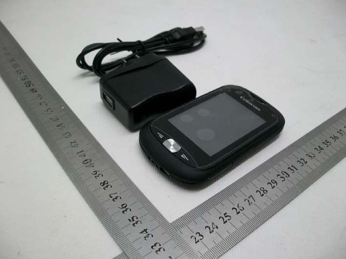
A2DA2T303G
Apr 01, 2013GSM Mobile Phone
Equipment Class
PCE - PCS Licensed Transmitter held to ear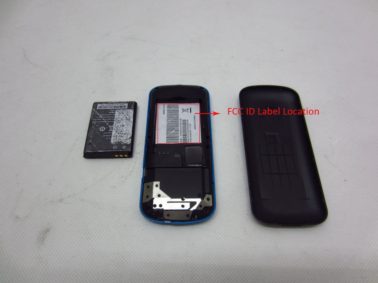
A2DA8T171AG
Mar 07, 2013GSM Mobile Phone
Equipment Class
JBP - Part 15 Class B Computing Device Peripheral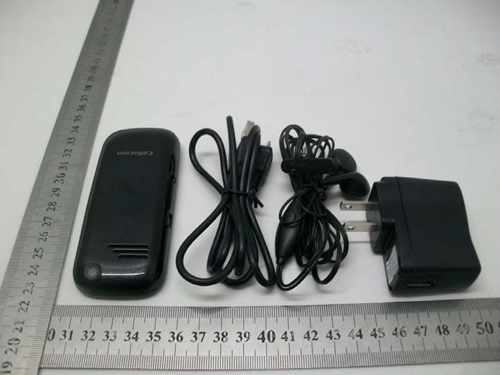
A2DA2T285G
Jan 23, 2013GSM Mobile Phone
Equipment Class
PCE - PCS Licensed Transmitter held to ear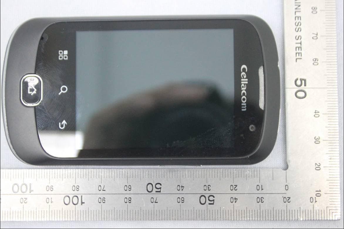
A2DA9T7013G
Nov 05, 20123G Mobile Phone
Equipment Class
DTS - Digital Transmission System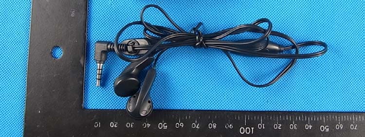
A2DA9T1183G
Jun 04, 2012Mobile Phone
Equipment Class
PCE - PCS Licensed Transmitter held to ear