A3LSMS918UPortable Handset
Samsung Electronics Co Ltd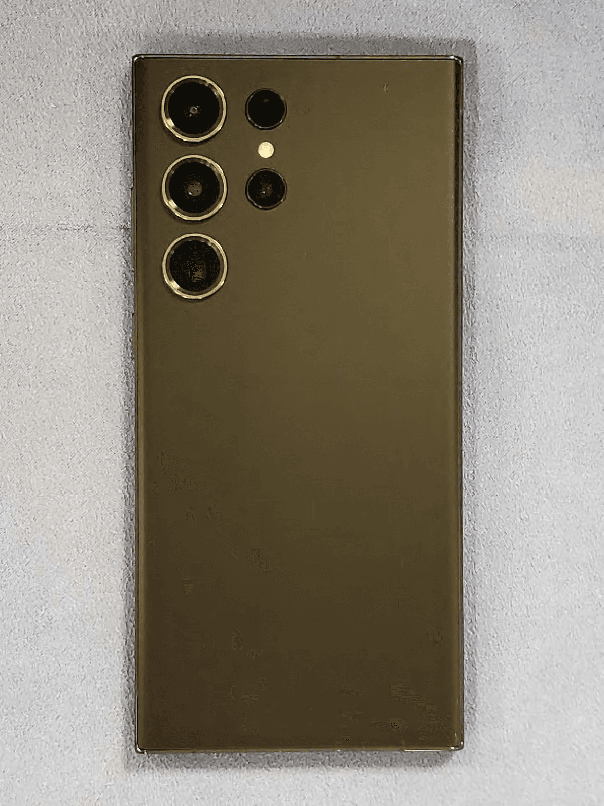
Click to zoom
Application Details
- Equipment Class
- 5GM - Part 30 Mobile Transmitter
- Date of Grant
- Dec 07, 2022
- Application Purpose
- Original Equipment
- Date of Application
- Nov 10, 2022
- Equipment Note
- Portable Handset
- Frequency Range
- 37000.00000000 - 40000.00000000
- Company
- Samsung Electronics Co Ltd
- Country
- United States
Documents & Files
Document Text
Text extracted from the exhibit documents filed with the FCC. Open a document above to read the original.
Users Manual
Quick Reference Guide (Terms an d Conditions) SM-S918U SM-S918U1 Read this document before operating the mobile device, accessories, or software (defined collectively and individually as the “Product”) and keep it for future reference. This document contains important Terms and Conditions. Electronic acceptance, opening the packaging, use, or retention of the Product constitutes acceptance of these Terms and Conditions. Visit www.samsung.com/us to view device information, the user manual, and more. You may incur additional charges for accessing the Internet. Device Layout To turn on the device, pr ess and hold th e Side key for a few seconds. The charger should remain close to the electric socket and easily accessible while charging. Installing a nano-SIM card Nano- SIM cards are sold separately. Contact us Questions? Visit us.community.samsung.com Get Support Call 1.800.SAMSUNG Service locations Find a service location near you at Samsung.com/us/support/service/locations Switching made simple Whether you are coming from an iOS or Android platform, you can easily transfer your data with Smart Switch. Back up your old phone Back up your old phone using your favorite back-up app. Samsung Smart Switch 1. From your new Galaxy device, tap Settings > Accounts and backup > Smart Switch. 2. Tap Receive data. 3. Select your old device type. 4. Tap Cable (Android) or Wireless (Android and iOS) and follow the prompts to connect your phones. Customize Tap Settings to personalize your phone. Flight mode This disables all wireless functions on your devic e. You can use only non- network services On the setting screen, tap Flight mode. NOTE: The use of Ultra-Wideband (UWB) transmitters is prohibited when aboard an aeroplane or ship. UWB Operation in airplane mode: UWB function is disabled when a phone get into the airplane mode. Important l egal information Arbitration Agreement - This Product is subject to a binding arbitrat ion agreement between you and SAMSUNG ELECTRONICS AMERICA, INC. (“Samsung”). You can opt out of t he agreement within 30 calendar days of the first consumer purchase by emailing [email protected] or calling 1-800-SAMSUNG (726-7864) and providing the applicable information. The full Arbitration Agreement, Standard One-year Limited Warranty, End User License Agreement (EULA), and Health & Safety Information for your device are available online: •English: www.samsung.com/us/Legal/Phone-HSGuide •Spanish: www.samsung.com/us/Legal/Phone-HSGuide-SP This information can also be found on the device in the “About device” or “About phone” or “About tablet” section, for example: •Settings > About phone or About device or About tablet > Legal information > Samsung legal •Or,Search “Legal” If your device required Federal Communications Commission (FCC) approval, you can view the FCC certification by opening Settings > About phone or About device or About tablet> Status Information Health and Safety WARNING! To avoid electri c shock and damage to your device, do not charge device while it is wet or in an area where it co uld get wet. Do not handle device, c harger or cords with wet hands while charging. Maint aining dust and water resistance The device is not impervious to dust and water damage in any situation. It is important that all c ompartments are closed tightly. Follow these tips carefully to prevent damage to the device and maintain dust and water resistance performance: •Water resistant based on IP68 rating, which tests submersion in fresh water deeper than 1.5 meters or keep it submerged for more than 30 minutes. If device is exposed to fresh water, dry it thoroughly with a clean, soft cloth; if exposed to liquid other than fresh water, rinse with fresh water and dry as directed. •Any device which uses accessible compar tments or por ts that can be opened should have these se aled or closed tightly to prevent liquid from entering th e system. •If the device has been immersed i n water or the microphone or speaker is wet, sound may not be heard clearly during a call. After wiping the device with a dry cloth, dry it thoroughly before using it. •Do not expose the device to water at high pressure. •If the device is dropped or receives an impact, the water and dust resistant features of the device may be damaged. Note: Liquid other than fresh water may enter the device fa ster. Failure to rinse the device in fresh water and dry it as instructed may cause the device to suffer from operability or cosmetic issues. Samsung Knox Samsung Knox is Samsung’s security platf orm. Additional licensing fees may be required for enterprise use. For more information about Knox, pl ease refer to: www.samsung.com/us/knox Specific Absorption Rate (SAR) certification information For information about SAR, visit : •https://www.fcc.gov/general/radio-frequency-safety-0 •www.fcc.gov/encyclopedia/ speci fic -absorption-rate-sar-cellular-telephones •www.samsung.com/sar Body-worn operations are restricted to belt-clips, holsters or similar accessories that have no metallic component in the assembly and must provide at least 1.5cm separation between the device and the user's body. Samsung Wireless Power Sharing feature allows device -to -device charging without the need for a charger. If your device supports the wireless power sharing function, this equipment should be operated with a minimum distance of 20 cm between the device and your body. Note: Foldable devices can be stored in an environment with ambient temperatures of -10°C / 14.0°F to 50°C / 122°F safely; prolonged exposure to temperatures outside these recommended temperatures can pose a high risk of damage to the device. Samsung mobile products and recycling WARNING! Never dispose of batteries in a fire because they may explode. Do not disassemble, crush, puncture, heat, burn or reuse. F or battery and cell phone recycling, go to call2re cycle. org or call 1- 800-822-8837. F or more recycling information, go to our website: www.samsung.com/re cycling …
Text truncated - open the document above for the full version.
Attestation Statements
Samsung Electronics America, Inc 19 Chapin Rd, Building D. Pine Brook, NJ 07058 Date: October 26, 2022 FCC ID: A3LSMS918U To whom it may concern: We, the undersigned, hereby authorize Element Washington DC LLC, to act on our behalf in all matters relating to applications for equipment authorization, including the signing of all documents relating to these matters. Any and all acts carried out by Element Washington DC LLC. on our behalf shall have the same effect as acts of our own. We also hereby certify that no party to any application is subject to a denial of benefits, including FCC benefits, pursuant to Section 5301 of the Anti-Drug Abuse Act of 1988, 21 U.S. C. 862. Sincerely, Jenni Chun / General Manager Samsung Electronics America, Inc. Address: 19 Chapin Rd., Building D Pine Brook, NJ 07058 Tel: 1-973-808-6375
Attestation Statements
SAMSUNG ELECTRONICS CO., LTD 129, Samsung-ro, Yeongtong-gu Suwon-si, Gyeonggi-do, 443-742 Korea October 20, 2022 Federal Communications Commission 7435 Oakland Mills Road Columbia, MD 21046 SUBJECT : Label Statement FCC ID : A3LSMS918U T o whom it may concern We hereby provide the following attestations according to CFR 2.935 and FCC KDB 784748 D02: A t the time of purchase, the FCC ID is readily and physically visible to the purchaser on the exterior package per CFR 2.935(f). The FCC ID will be readily legible without the aid of magnification according to CFR 2.935(d). The literature in the package describes how to access the electronic display to find the FCC ID per CRF 2.935(b) and FCC KDB 784748. Per CFR 2.935(c), the user will be able to access this information within a maximum of 3 steps. The user will be able to access this information without a SIM card, special accessories or supplemental plug-ins. Per CFR 2.935(e), We, Samsung have programmed the e-label and it is not able to be modified by any third party. P er CFR 2.935(f), the FCC ID will be able to survive normal shipping and handling so it is visible for inspection at the time of import. S hould you have any questions or comments concerning the above, please contact the undersigned. S incerely Yours, J enni Chun/ General Manager Samsung Electronics America. Inc Address: 19 Chapin Rd., Building D Pine Brook, NJ 07058 Tel: 1-973-808-6375
Cover Letter(s)
SAMSUNG ELECTRONICS AMERICA, INC. American QA Lab 19 Chapin Rd, Building D. Pine Brook, NJ 07058 Date: October 26, 2022 Federal Communications Commission Authorization and Evaluation Division 7435 Oakland Mills Road, Columbia, MD 21046 RE:Request of Confidentiality for FCC ID: A3LSMS918U To Whom It May Concern: Pursuant to Sections 0.457 and 0.459 of the Commission’s Rules (CFR 47), and Section 552 (b) (4) of the Freedom of Information Act, SAMSUNG ELECTRONICS CO.,LTD. hereby requests confidentiality and treatment of certain information accompanying this application. The materials contain trade secrets and proprietary information not customarily re leased to th e public. The public disclosure of these matters might be harmful to the Applicant and provide unjustified benefits to its competitors. We are also hereby request Short-Term Confidentiality for 180 days after the grant as outlined in Public Notice DA 04-1705. This provision will give SAMSUNG ELECTRONICS CO.,LTD. temporary confidentiality of commercially sensitive information prior to product release. The requested Permanent and Short-Term Confidential exhibits are listed as follows: PERMANENT AND SHORT-TERM CONFIDENTIAL LIST ExhibitDescription PERMANENT 1 Block Diagram 2 Operational Description 3 Schematics 4 Parts List & Tune-Up Procedure SHORT-TERM 5 External Photos 6 Internal Photos 7 Test-Setup Photos 8 Users Manual The Applicant understands that pursuant to Rule 0.457, disclosure of this application and all accompanying documentations, where applicable, will not be made public before the date of the Grant for this application. Sincerely, Jenni Chun / General Manager Samsung Electronics America, Inc. Address: 19 Chapin Rd., Building D Pine Brook, NJ 07058 Tel: 1-973-808-6375
External Photos
FCC ID: A3LSMS918U External Photographs FCC ID: A3LSMS918U External Photographs FCC ID: A3LSMS918U External Photographs FCC ID: A3LSMS918U External Photographs FCC ID: A3LSMS918U External Photographs FCC ID: A3LSMS918U External Photographs FCC ID: A3LSMS918U External Photographs FCC ID: A3LSMS918U External Photographs FCC ID: A3LSMS918U External Photographs
ID Label/Location Info
Description of E-label on the A3LSMS918U Date: October 20, 2022 FCC ID: A3LSMS918U Thi s model is applied E-label, please find description of E-label below. 1. FCC ID (E-label): Settings > About Phone > Status Information F CC certification FCC ID: A3LSMS918U <Device Display Screen> 2.FCC ID on the Quick Start Guide The FCC has granted an Equipment Authorization for this model device based on the compliance of all reported SAR levels with the FCC RF exposure guide lines. This device has a FCC ID number A3LSMS918U [Model Number: SM-S918U, SM-S918U1] and the specific SAR levels for this device can be found at the following. FCC website: www.fcc.gov/oet/ea/ The SAR information for this device can be found on Samsung’s w ebsite: www.samsung.com/sar
Internal Photos
FCC ID: A3LSMS918U Internal Photographs FCC ID: A3LSMS918U Internal Photographs FCC ID: A3LSMS918U Internal Photographs FCC ID: A3LSMS918U Internal Photographs FCC ID: A3LSMS918U Internal Photographs FCC ID: A3LSMS918U Internal Photographs FCC ID: A3LSMS918U Internal Photographs FCC ID: A3LSMS918U Internal Photographs FCC ID: A3LSMS918U Internal Photographs FCC ID: A3LSMS918U Internal Photographs FCC ID: A3LSMS918U Internal Photographs
RF Exposure Info
FCC ID: A3LSMS918U Power Density Simulation Report Revision A November 07, 2022 SAMSUNG ELECTRONICS 1. Simulation methodology for Power Density (PD) 1.1 Simulation tool 1.1.1 Tool description For the simulation approach to calculating power density (PD) evaluation for mobile phone with mmWave antenna modules, ANSYS Electromagnetics suite version 2022.R1 (HFSS) is used. ANSYS HFSS is one of several commercial tools for 3D full-wave electromagnetic simulation used for antenna and RF structure design of high frequency component. ANSYS Electromagnetics suite version 2022.R1 (HFSS) is implemented based on Finite Element Method (FEM), which operates in the frequency domain. 1.1.2 Mesh and Convergence criteria To solve the PD analysis using FEM, volume area containing simulated objects should be subdivided into electrically small parts that are called finite elements as the unknown functions. To subdivide system, the adaptive mesh technique in ANSYS Electromagnetics suite version 2022.R1 (HFSS) is used. ANSYS Electromagnetics suite version 2022.R1 (HFSS) starts to refine the initial mesh based on wavelength and calculate the error to iterative process for adaptive mesh refinement. The determination parameter of the number of iteration in ANSYS Electromagnetics suite version 2022.R1 (HFSS) is defined as convergence criteria, delta S, and the iterative adaptive mesh process repeats until the delta S is met. In ANSYS Electromagnetics suite version 2022.R1 (HFSS), the accuracy of converged results depends on the delta S. Figure 1 is an example of adaptive mesh of the device (cross-section of top view). Figure 1 Example of the adaptive mesh technique (Top view) 1.1.3 Power density calculation After solving 3D full-wave electromagnetic simulation, various kinds of physical quantities can be obtained. To calculate PD evaluation, two physical quantities, an electric field (E ��⃗ ) and a magnetic field (H ��⃗ ) are needed. The actual consumption power can be expressed as the real term of the Poynting vector (S �⃗ ) from the cross product of E ��⃗ and complex conjugation of H ��⃗ as shown below: 〈 S �⃗ 〉 =Re� 1 2 E ��⃗ × H ��⃗ ∗ � 〈 S �⃗ 〉 can be expressed as point power density based on a peak value of each spatial point on mesh grids, and obtained directly from ANSYS Electromagnetics suite version 2022.R1 (HFSS). From the point power density 〈 S �⃗ 〉 , the spatial-averaged power density (PD 푎푎푎푎 ) on an evaluated area (A) can be derived as shown below: PD 푎푎푎푎 = 1 퐴퐴 � 〈 S �⃗ 〉 ∙푑푑푑푑= 퐴퐴 1 2퐴퐴 푎푎푎푎 � ‖ 푅푅푅푅 { 퐸퐸퐸퐸퐻퐻 ∗ }‖ 퐴퐴 푎푎푎푎 푑푑퐴퐴 , where the spatial-averaged power density (PD 푎푎푎푎 ) is total power density value considering on x, y and z components of point power density 〈 S �⃗ 〉 and the evaluated area (A) is 4cm 2 . 1.2 Simulation setup 1.2.1 3D modeling Figure 2 shows the simulation model which is mounted two mmWave antenna modules. The simulation modeling includes most of the entire structure of device itself such as PCB, metal frame, battery, cables, and legacy antennas as well as mmWave antenna modules called as Ant M and Ant N. The modeling contains the entire EUT to enable a Smart transmit GEN2, as well. Ant M is placed on the left side and antennas are facing the back side, and Ant N is placed on the right side and antennas are facing the right side of the device. Figure 2 Simulation model which is mounted two mmWave antenna modules 1.2.2 PD evaluation planes Table 1 shows the PD evaluation planes for each mmWave antenna module and Figure 3 shows the PD evaluation planes and truncation area of the simulation model to find worst case of beamforming cases. Please note that the “right” and “left” edge of mentioned in this report are defined from the perspective of looking at the device from the front side. Table 1. PD evaluation planes Module Front Back Left From Front View Right From Front View To p Bottom S1 S2 S3 S4 S5 S6 Ant M O O O O O O Ant N O O O O O O Figure 3. PD evaluation planes 1.2.3 Boundary condition To simulate electromagnetic tool based on FEM, the boundary condition allows electromagnetic waves to be electrically open at the boundary and radiated far away without reflection. ANSYS Electromagnetics suite version 2022.R1 (HFSS) can support the absorbing boundary condition (ABC) for radiation boundary and make normally a quarter wave length from the radiating structure. In this report, to cover all beamforming cases of mmWave antenna modules, 40 mm spacing from the device for each surfaces were adopted. This distance is sufficiently large enough for “Qualcomm MG script” to extract valid E- and H-fields from all adjacent exposure surfaces of the EUT. 1.2.4 Source excitation condition The number of antenna ports of ANT M and ANT N for source excitation are the same. The antenna port of ANT M and N is divided into 10 ports for n261 and n258 1 x 5 patch array antennas, 10 ports for n260 1 x 5 patch array antennas. In the 10 ports included in each patch antenna, 5 ports are divided into vertical polarization feeding, and the other 5 ports are divided into horizontal polarization feeding. Figure 4 shows the ANT M module structure and surrounding structure. The ANT M module is encrypted in the ANSYS Electromagnetics suite (HFSS) and can only check the feeding position. Figure 4. mmWave module (ANT M) After finishing 3D full wave electromagnetic simulation of modeling structure, the magnitude and phase information can be loaded for each port by using “Edit Sources” function in ANSYS Electromagnetics suite (HFSS). Figure 5 shows an example of antenna port excitations. Figure 5. An example of port excitation (ANT N) Since ANSYS Electromagnetics suite (HFSS) uses FEM solver based on frequency domain analysis method, the input source for the port excitation applies sinusoidal waveform for each frequency. 1.2.5 Condition of simulation completion The simulation completion condition of ANSYS Electromagnetics suite (HFSS) is defined as delta S. The ANSYS Electromagnetics suite (HFSS) calculates …
Text truncated - open the document above for the full version.
RF Exposure Info
APPENDIX A: POWER DENSITY TEST PLOTS A1 Element Date: 09/20/2022 Antenna M Beam 153; H; High Ch.; CW Device Under Test Properties DUT Serial Number DUT Type A3LSMS918U VHT0152M Portable Handset Exposure Conditions Phantom Section Position Test Distance [mm] Band Frequency [MHz] 5G BACK 2.00 n258 25200.00 Hardware Setup Probe, Calibration Date DAE, Calibration Date EUmmWV4 – SN9541, 05/19/2022 DAE4ip SN1638, 11/11/2021 Software Setup Software Software Version cDASY6 Module mmWave 3.0.0.841 Scans Setup Scan Type 5G Scan Grid Extents [mm] 80x80 Grid Steps [lambda] 0.25 x 0.25 Sensor Surface [mm] 2.0 Measurement Results Scan Type 5G Scan Avg. Area [cm 2 ] 4.00 pS tot avg [W/m 2 ] 4.64 pS n avg [W/m 2 ] 3.77 E peak [V/m] 69.6 Power Drift [dB] -0.03 A2 Element Date: 09/20/2022 Antenna N Beam 169; H; Low Ch.; CW Device Under Test Properties DUT Serial Number DUT Type A3LSMS918U VHT0167M Portable Handset Exposure Conditions Phantom Section Position Test Distance [mm] Band Frequency [MHz] 5G BACK 2.00 n258 24350.00 Hardware Setup Probe, Calibration Date DAE, Calibration Date EUmmWV3 – SN9407, 12/13/2021 DAE4ip SN1639, 01/21/2022 Software Setup Software Software Version cDASY6 Module mmWave 3.0.0.841 Scans Setup Scan Type 5G Scan Grid Extents [mm] 80x80 Grid Steps [lambda] 0.25 x 0.25 Sensor Surface [mm] 2.0 Measurement Results Scan Type 5G Scan Avg. Area [cm 2 ] 4.00 pS tot avg [W/m 2 ] 4.27 pS n avg [W/m 2 ] 3.66 E peak [V/m] 56.7 Power Drift [dB] -0.19 A3 Element Date: 09/20/2022 Antenna M Beam 165; H; Low Ch.; CW Device Under Test Properties DUT Serial Number DUT Type A3LSMS918U VHT0152M Portable Handset Exposure Conditions Phantom Section Position Test Distance [mm] Band Frequency [MHz] 5G BACK 2.00 n261 27550.10 Hardware Setup Probe, Calibration Date DAE, Calibration Date EUmmWV4 – SN9541, 05/19/2022 DAE4ip SN1638, 11/11/2021 Software Setup Software Software Version cDASY6 Module mmWave 3.0.0.841 Scans Setup Scan Type 5G Scan Grid Extents [mm] 80x80 Grid Steps [lambda] 0.25 x 0.25 Sensor Surface [mm] 2.0 Measurement Results Scan Type 5G Scan Avg. Area [cm 2 ] 4.00 pS tot avg [W/m 2 ] 4.85 pS n avg [W/m 2 ] 3.36 E peak [V/m] 72.8 Power Drift [dB] -0.01 A4 Element Date: 10/13/2022 Antenna N Beam 158; H; High Ch.; CW Device Under Test Properties DUT Serial Number DUT Type A3LSMS918U VHT0152M Portable Handset Exposure Conditions Phantom Section Position Test Distance [mm] Band Frequency [MHz] 5G RIGHT 2.00 n261 28300.00 Hardware Setup Probe, Calibration Date DAE, Calibration Date EUmmWV4 – SN9541, 05/19/2022 DAE4ip SN1639, 01/21/2022 Software Setup Software Software Version cDASY6 Module mmWave 3.0.0.841 Scans Setup Scan Type 5G Scan Grid Extents [mm] 80x80 Grid Steps [lambda] 0.25 x 0.25 Sensor Surface [mm] 2.0 Measurement Results Scan Type 5G Scan Avg. Area [cm 2 ] 4.00 pS tot avg [W/m 2 ] 5.04 pS n avg [W/m 2 ] 4.29 E peak [V/m] 86.0 Power Drift [dB] -0.15 A5 Element Date: 09/20/2022 Antenna M Beam 154; H; Mid Ch.; CW Device Under Test Properties DUT Serial Number DUT Type A3LSMS918U VHT0152M Portable Handset Exposure Conditions Phantom Section Position Test Distance [mm] Band Frequency [MHz] 5G BACK 2.00 n260 38500.00 Hardware Setup Probe, Calibration Date DAE, Calibration Date EUmmWV4 – SN9541, 05/19/2022 DAE4ip SN1638, 11/11/2021 Software Setup Software Software Version cDASY6 Module mmWave 3.0.0.841 Scans Setup Scan Type 5G Scan Grid Extents [mm] 80x80 Grid Steps [lambda] 0.25 x 0.25 Sensor Surface [mm] 2.0 Measurement Results Scan Type 5G Scan Avg. Area [cm 2 ] 4.00 pS tot avg [W/m 2 ] 5.40 pS n avg [W/m 2 ] 4.57 E peak [V/m] 81.6 Power Drift [dB] 0.06 A6 Element Date: 09/20/2022 Antenna N Beam 41; V; Low Ch.; CW Device Under Test Properties DUT Serial Number DUT Type A3LSMS918U VHT0167M Portable Handset Exposure Conditions Phantom Section Position Test Distance [mm] Band Frequency [MHz] 5G RIGHT 2.00 n260 37050.00 Hardware Setup Probe, Calibration Date DAE, Calibration Date EUmmWV3 – SN9407, 12/13/2021 DAE4ip SN1639, 01/21/2022 Software Setup Software Software Version cDASY6 Module mmWave 3.0.0.841 Scans Setup Scan Type 5G Scan Grid Extents [mm] 80x80 Grid Steps [lambda] 0.25 x 0.25 Sensor Surface [mm] 2.0 Measurement Results Scan Type 5G Scan Avg. Area [cm 2 ] 4.00 pS tot avg [W/m 2 ] 4.06 pS n avg [W/m 2 ] 3.38 E peak [V/m] 80.3 Power Drift [dB] 0.20
RF Exposure Info
APPENDIX B: POWER DENSITY SYSTEM VERIFICATION PLOTS B1 Element Date: 09/20/2022 30 GHz System Verification Device Under Test Properties DUT Serial Number 30 GHz Verification Source 1045 Exposure Conditions Phantom Section Position Test Distance [mm] Band Frequency [MHz] 5G FRONT 5.55 Validation band 30000.0 Hardware Setup Probe, Calibration Date DAE, Calibration Date EUmmWV4 – SN9541, 05/19/2022 DAE4ip SN1638, 11/11/2021 Software Setup Software Software Version cDASY6 Module mmWave 3.0.0.841 Scans Setup Scan Type 5G Scan Grid Extents [mm] 60.0 x 60.0 Grid Steps [lambda] 0.25 x 0.25 Sensor Surface [mm] 5.55 Measurement Results Scan Type 5G Scan Avg. Area [cm 2 ] 4.00 pS tot avg [W/m 2 ] 36.3 pS n avg [W/m 2 ] 35.8 E peak [V/m] 137 Deviation (dB) 0.45 30 GHz System Verification Calibration Certificate B2 Element Date: 09/20/2022 30 GHz System Verification Device Under Test Properties DUT Serial Number 30 GHz Verification Source 1035 Exposure Conditions Phantom Section Position Test Distance [mm] Band Frequency [MHz] 5G FRONT 5.55 Validation band 30000.0 Hardware Setup Probe, Calibration Date DAE, Calibration Date EUmmWV3 – SN9407, 12/13/2021 DAE4ip SN1639, 01/21/2022 Software Setup Software Software Version cDASY6 Module mmWave 3.0.0.841 Scans Setup Scan Type 5G Scan Grid Extents [mm] 60.0 x 60.0 Grid Steps [lambda] 0.25 x 0.25 Sensor Surface [mm] 5.55 Measurement Results Scan Type 5G Scan Avg. Area [cm 2 ] 4.00 pS tot avg [W/m 2 ] 29.4 pS n avg [W/m 2 ] 29.0 E peak [V/m] 123 Deviation (dB) -0.42 30 GHz System Verification Calibration Certificate B3 Element Date: 10/11/2022 30 GHz System Verification Device Under Test Properties DUT Serial Number 30 GHz Verification Source 1035 Exposure Conditions Phantom Section Position Test Distance [mm] Band Frequency [MHz] 5G FRONT 5.55 Validation band 30000.0 Hardware Setup Probe, Calibration Date DAE, Calibration Date EUmmWV4 – SN9622, 02/24/2022 DAE4 SN1676, 06/15/2022 Software Setup Software Software Version cDASY6 Module mmWave 3.0.0.841 Scans Setup Scan Type 5G Scan Grid Extents [mm] 60.0 x 60.0 Grid Steps [lambda] 0.25 x 0.25 Sensor Surface [mm] 5.55 Measurement Results Scan Type 5G Scan Avg. Area [cm 2 ] 4.00 pS tot avg [W/m 2 ] 29.3 pS n avg [W/m 2 ] 28.9 E peak [V/m] 122 Deviation (dB) -0.44 30 GHz System Verification Calibration Certificate B4 Element Date: 10/31/2022 30 GHz System Verification Device Under Test Properties DUT Serial Number 30 GHz Verification Source 1045 Exposure Conditions Phantom Section Position Test Distance [mm] Band Frequency [MHz] 5G FRONT 5.55 Validation band 30000.0 Hardware Setup Probe, Calibration Date DAE, Calibration Date EUmmWV4 – SN9541, 05/19/2022 DAE4ip SN1639, 01/21/2022 Software Setup Software Software Version cDASY6 Module mmWave 3.0.0.841 Scans Setup Scan Type 5G Scan Grid Extents [mm] 60.0 x 60.0 Grid Steps [lambda] 0.25 x 0.25 Sensor Surface [mm] 5.55 Measurement Results Scan Type 5G Scan Avg. Area [cm 2 ] 4.00 pS tot avg [W/m 2 ] 37.0 pS n avg [W/m 2 ] 36.6 E peak [V/m] 137 Deviation (dB) 0.54 30 GHz System Verification Calibration Certificate
RF Exposure Info
APPENDIX D: PROBE AND VERIFICATION SOURCE CALIBRATION CERTIFICATES
RF Exposure Info
FCC ID: A3LSMS918U PART 2 RF EXPOSURE EVALUATION REPORT Approved by: Technical Manager Document S/N: DUT Type: Page 1 of 76 1M2209010098-04.A3L Portable Handset © 2022 Element REV 1.0 04/06/2020 Unless otherwise specified, no part of this report may be reproduced or utilized in any part, form or by any means, electronic or mechanical, including photocopying and microfilm, without permission in writing from Element. If you have any questions or have an enquiry about obtaining additional rights to this report or assembly of contents thereof, please contact [email protected]. Applicant Name: Date of Testing: Samsung Electronics Co., Ltd. 09/30/2022 – 11/14/2022 129, Samsung-ro, Maetan dong, Test Site/Location: Yeongtong-gu, Suwon-si Element, Columbia, MD, USA Gyeonggi-do, 16677, Korea Document Serial No.: 1M2209010098-04.A3L FCC ID: A3LSMS918U APPLICANT: SAMSUNG ELECTRONICS CO., LTD. DUT Type: Portable Handset Application Type: Certification FCC Rule Part(s): CFR §2.1093 Model: Additional Model: Device Serial Numbers: SM-S918U SM-S918U1 Pre-Production Samples [0329M, 0347M, 1451M, 0265M] I attest to the accuracy of data. All measurements reported herein were performed by me or were made under my supervision and are correct to the best of my knowledge and belief. I assume full responsibility for the completeness of these measurements and vouch for the qualifications of all persons taking them. Test results reported herein relate only to the item(s) tested. Element (formerly PCTEST) 7185 Oakland Mills Road, Columbia, MD 21046 USA Tel. +1.410.290.6652 / Fax +1.410.290.6654 http://www.element.com PART 2 RF EXPOSURE EVALUATION REPORT FCC ID: A3LSMS918U PART 2 RF EXPOSURE EVALUATION REPORT Approved by: Technical Manager Document S/N: DUT Type: Page 2 of 76 1M2209010098-04.A3L Portable Handset © 2022 Element REV 1.0 04/06/2020 Unless otherwise specified, no part of this report may be reproduced or utilized in any part, form or by any means, electronic or mechanical, including photocopying and microfilm, without permission in writing from Element. If you have any questions or have an enquiry about obtaining additional rights to this report or assembly of contents thereof, please contact [email protected]. TABLE OF CONTENTS 1 DEVICE UNDER TEST .................................................................................................................................3 2 RF EXPOSURE LIMITS ................................................................................................................................6 3 TIME VARYING TRANSMISSION TEST CASES .........................................................................................8 4 FCC MEASUREMENT PROCEDURES (FREQ < 6 GHZ) ........................................................................ 12 5 FCC MEASUREMENT PROCEDURES (FREQ > 6 GHZ) ........................................................................ 25 6 MEASUREMENT TEST SETUP (FREQ < 6 GHZ) .................................................................................... 34 7 MEASUREMENT TEST SETUP (FREQ > 6 GHZ) .................................................................................... 37 8 TEST CONFIGURATIONS (FREQ < 6 GHZ) ............................................................................................. 39 9 CONDUCTED TX CASES (FREQ < 6 GHZ).............................................................................................. 44 10 TEST CONFIGURATIONS (FREQ > 6 GHZ) ............................................................................................. 62 11 RADIATED POWER TX CASES (FREQ > 6 GHZ) .................................................................................... 65 12 SYSTEM VERIFICATION (FREQ > 6 GHZ) .............................................................................................. 70 13 EQUIPMENT LIST ...................................................................................................................................... 71 14 MEASUREMENT UNCERTAINTIES.......................................................................................................... 72 15 CONCLUSION ............................................................................................................................................ 74 16 REFERENCES ........................................................................................................................................... 75 APPENDIX A: VERIFICATION PLOTS APPENDIX B: TEST SETUP PHOTOGRAPHS APPENDIX C: TEST SEQUENCES APPENDIX D: TEST PROCEDURES FOR SUB6 NR + NR RADIO APPENDIX E: CALIBRATION CERTIFICATES FCC ID: A3LSMS918U PART 2 RF EXPOSURE EVALUATION REPORT Approved by: Technical Manager Document S/N: DUT Type: Page 3 of 76 1M2209010098-04.A3L Portable Handset © 2022 Element REV 1.0 04/06/2020 Unless otherwise specified, no part of this report may be reproduced or utilized in any part, form or by any…
Text truncated - open the document above for the full version.
Contact Information
Applicant
Jenni Chun(General Manager)
Test Firm
Element Materials Technology Washington DC LLCZach Keyser
[email protected]1111111111
Technical Specifications
| # | Rule Parts | Frequency Range | Power Output | Emission | Tolerance |
|---|---|---|---|---|---|
| 16 | 3 | 37.00 GHz - 40.00 GHz | 251.00 mW | 396MW7D | 2.5 ppm |
Other Applications from Samsung Electronics Co Ltd
A3LSMU600
Sep 15, 2026Bluetooth Headset
Equipment Class
DTS - Digital Transmission SystemA3LSMA185G
Sep 08, 2026Portable Handset
Equipment Class
CXX - Communications Rcvr for use w/ licensed Tx and CBsA3LSMS741B
Aug 05, 2026Portable Handset
Equipment Class
6VL - 15E 6 GHZ Very Low Power DeviceA3LSMX940
Jul 31, 2026BT,BLE Tablet DTS,UNII a,b,g,n,ac,ax,be and digitizer
Equipment Class
DTS - Digital Transmission SystemA3LSMS741U
Jul 30, 2026Portable Handset
Equipment Class
6CD - 15E 6 GHz Low Power Dual Client