A5MW770LENOVO WIRELESS HEADSET W770 (HEADSET)
Lenovo (Beijing) Limited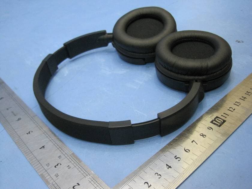
Click to zoom
Application Details
- Equipment Class
- DSS - Part 15 Spread Spectrum Transmitter
- Date of Grant
- Dec 26, 2011
- Application Purpose
- Original Equipment
- Date of Application
- Dec 26, 2011
- Equipment Note
- LENOVO WIRELESS HEADSET W770 (HEADSET)
- Frequency Range
- 2404.00000000 - 2476.00000000
- Company
- Lenovo (Beijing) Limited
- Country
- China
Documents & Files
Document Text
Text extracted from the exhibit documents filed with the FCC. Open a document above to read the original.
Users Manual
W770 Wireless Headset W770 Wireless Headset User Manual User Manual W770 Wireless Headset Product name: Lenovo Wireless Headset W770 Product standard: Q/HDLCS103-2009 Manufacturer: Lenovo (Beijing) Limited Address: No.6 Chuang Ye Road, Shangdi Information Industry Base, Haidian District, Beijing, China Zip Code: 100085 Lenovo website: www.lenovo.com W770 Wireless Headset User Manual ― 1 ― I. PRODUCT INTRODUCTION Dear customers, Thank you for selecting high-quality electronic product offered by Lenovo. This headset is manufactured with internationally advanced 2.4 GHz wireless audio transmission technology. This technology is characterized by stable signal (easily avoiding the interference of other signals with high frequency hopping anti-interference technology), long transmission distance and Hi-fi stereo. This headset consists of one USB Dongle and one receiver (headset). Its in-built Lithium polymer battery of 380 mAh provides a standby time of 6 hours, allowing you enjoy the music and chat online freely. OS requirement: WIN XP, WIN 2000, WIN 7, VISTA, Apple MAC Compatible players: MediaPlayer, RealPlayer, etc. W770 Wireless Headset User Manual ― 2 ― II. INTRODUCTION Of heaDSeT CONNeCTION 1. First, connect the USB Dongle to the USB interface of the computer. The computer will automatically recognize the USB Dongle. After it prompts that the device installation is completed, the device can be used normally (with the computer providing tips for first use). 2. Turn on the headset. After it completes connection with the USB Dongle, the headset can be used normally. III. heaDSeT bUTTONS On/Off Charging Indicator Charging Port To ggle Switch Working State Indicator 1. On/Off a. Power On: By pressing this button for over 1 second in power off state, blue LED lamp is constantly on, and the headset is started. b. Power Off: By pressing this button for over 1 second and then releasing it in power on or playing state, blue LED lamp is off, and the headset is powered off. 2. Toggle switch a. Pause/Play: In playing state, press middle part of this button to pause, and press middle part of this button again to resume the playing. b. Previous/Next: Press this button and hold for a moment to play the previous/next song. c. Volume +/-: Toggle this button upwards/downwards to increase/decrease the volume. W770 Wireless Headset User Manual ― 3 ― IV. INDICaTOR LamP 1. Red LeD lamp Red LED lamp is the charging indicator. It lights on when the device is charged, and is off when the charging completes (or low level lighting). 2. blue LeD lamp Blue LED lamp is the working state indicator. a. When power on, this lamp is on indicating the device works normally; b. This lamp is off when the device is powered off or the battery is out of power. V. mICROPhONe The microphone is hidden multi-directional microphone, providing superior gaming and chatting experience. Microphone VI. ChaRgINg INSTRUCTIONS Charging port Charging cable W770 Wireless Headset User Manual ― 4 ― 1. Connect 3.5 mm charging plug with the headset first, and connect USB connector of the charging cable with USB port of the computer or USB port of dedicated charger. Red LED lamp is on and the device enters the charging state. 2. When the charging is completed, red LED lamp is off. You could just disconnect the charging cable. Notes: ● This headset is equipped with inbuilt irremovable charging battery. Please do not remove the battery to avoid the damage to the headset. ● The charging time of the headset battery for the first time should be 12 - 24 hours to activate the best operating state of the battery. Later on, the charging time will be 2 - 3 hours (please do not charge the device for over 24 hours to avoid the damage to the service life of the battery). ● This 3.5 mm plug can only be used for connecting the charging port of over W770, but cannot connect the audio port of the audio device such as PC. VII. WeaRINg INSTRUCTIONS 1. Please distinguish the left and right side of the headset when wearing it: “L” on the bracket indicates the left side, while “R” indicates the right side. 2. Both sides of the headset are equipped with collapsible headphones. The length can be adjusted accordingly to make you enjoy the music comfortably! The stretched length is 24±1 mm. W770 Wireless Headset User Manual ― 5 ― VIII. ROTaTINg eaR PaD 90 degrees of rotation IX. faQS 1. No sound can be heard a. Check whether the USB Dongle has been plugged in USB port of the computer, and the microphone has been powered on; b. Adjust the volume with the toggle switch on the headset; c. Close and reopen the multimedia player; d. Check the headset power and charge it if low; e. If the problem persists, please re-match it by following the matching instruction. (Matching instruction: Press and hold “On/Off” button for over 15 seconds when the headset is powered on, and blue LED lamp flashes quickly and beeps. At this point, the headset enters the searching state and the matching begins. Blue LED lamps will be on constantly when the matching is completed. The best matching distance is 20 cm - 50 cm.) 2. Short receiving range Check whether there are other devices at the same frequency beside USB Dongle, and move USB Dongle to an open place. 3. During the use, you may hear sizzling sound in the headset or experience an interruption due to the interference from your surrounding wireless devices or screening of obstacles. Note: If the headset can not be powered on, the reason may be low power after long time with no use. In this case, please charge it first. W770 Wireless Headset User Manual ― 6 ― X. PRODUCT PaRameTeR headset: Drive unit ...............................................................................................................2 x 40 mm Frequency response ........................................................................................20Hz ~ 20KHz Impedance ................................................................................................32Ω…
Text truncated - open the document above for the full version.
Block Diagram
PCBantenna LDO Power_Control_Out GND 16MHz PLAY ROUT Power_Control_In IA2EH VOL_DN LOUT EEPROM VBUS MIC_IN VOL_UP Module Block Diagram VBAT CodecWM8988 ID/Sync_LED IA2EH Headset RX Module An-Tek Technology Corp. PGND VDT GPIO26GPIO33 BCD 1 Size:Document Name: Rev: Date: Sheet: 1 of 1 A320111111 V1.0 IA2EH_Headest TX_Block BLOCK Company: Sheet Name: Drawing: Hanks An-tek Electrionics Technology Co.,Ltd Charge Jack Charge Chip PJ4054 5V InputBattery Input VBUS VDT_EN PMOS ROUTLOUT MIC-INPLAYVOL_DNVOL_UP Power on/off/ Circuit Power on/off switch Power_Control_Out Power_Control_In D1,D2,Q2,Q4 ID/Sync_LEDCharge LED GND DC BOLCK SP-R SP-L MicrophoneSpeaker Speaker Slide Switch KeySwitchLed Lamp System Board Block Diagram PMOS
External Photos
2.1 Product View 2.2 EUT – Appearance View
ID Label/Location Info
Page: 48 of 48 Lenovo (Beijing) Limited FCC ID: A5MW770 The results shown in this test report refer only to the sample(s) tested , This Test report cannot be reproduced, except in full, without prior written permission of the Company. WALTEK SERVICES Reference No.: WT11116684-D-E-F 17 FCC Label This device complies with Part 15 of the FCC Rules. Operation is subject to the following two conditions: (1) this device may not cause interference, and (2) this device must accept any interference, including interference that may cause undesired operation of the device. The Label must not be a stick-on paper. The Label on these products must be permanently affixed to the product and readily visible at the time of purchase and must last the expected lifetime of the equipment not be readily detachable. Proposed Label Location on EUT EUT Top View/ proposed FCC Label Location FCC ID: A5MW770 This device complies with Part 15 of the FCC Rules. Operation is subject to the following two conditions: (1) this device may not cause harmful interference, and (2) this device must accept any interference received, including interference that may cause undesired operation.
ID Label/Location Info
FCC ID Label Sample for Model: W770 FCC ID: A5MW770 This device complies with Part 15 of the FCC Rules. Operation is subject to the following two conditions: (1) this device may not cause harmful interference, and (2) this device must accept any interference received, including interference that may cause undesired operation.
Internal Photos
2.1 EUT – Open View 2.2 EUT – PCB View 2.3 Battery - View
Operational Description
Circuit Description In the headset, the 2.4GMHz wireless module is build into receiver, the transceiver and audio process IC is control by IA2EH, which utilize a 16MHz OSC. Audio codec process IC is control by WM8999. Power management IC which supply the PCB Power for receiver is control by SGM2007. 3.7V li-ion battery is build into receiver, charging management IC is control by PJ4054, and the charging status will show by LED function. Other switch and LED is for how to use the receiver and display the status for user reference. The working procedures are: 1. When power on, the headset will scan the whole frenquency band again and again until a connection command sent by the USB Dongle is received. 2. The headset transmit a response signal. 3. The USB Dongle receive the response signal and recognize it, then send a connection command to build up the connect. 4. While the connection build up successfully, the data transmission is beginning. At the same time, the USB dongle and device (headset) will shift frequencies in synchronization per a same pseudo randomly ordered list of hopping frequencies, the hopping rate is 250 times per second. 5. The bandwidth of the headset, which is set to a fix width by the software, match the hopping channel bandwidth of their corresponding transmitter.
Schematics
55 44 33 22 11 D D C C B B A A Power Low battery detect Low battery detection for 3.2V POWER / GND 2 IA2EH Core Module RX Custom 1 3 Tuesday, December 21, 2010 TitleSize Document Number Rev Date: Sheet of VDC VDT_IN PGND VCC_Codec PGND PGND PGND PGND PGND VBUS VCC PGND VBAT PGND PGND PGND VBAT PGND PGND B10RL_0603 R651.5KR_0402 C1420.1uFC_0402 R424.3KR_0402 TP16TP_1.2MM R665.6KR_0402 + C9547uFTC_3528 U8SGM2007SOT-23-5 123 45 INGNDEN BYPASS OUT C770.1uFC_0402 + C1474.7uFC_0603 B310RL_0603 Q1GSM9105ZFSOT-23R6420KR_0402 + C814.7uFC_0603 C14110nFC_0402 C1404.7uFC_0603 + C154NCTC_3216 C123NC/ESDC_0402 55 44 33 22 11 D D C C B B A A EEPROM AT24C64 RF trace : 26mil width/6mil clearance for40mil thickness PCB16MHz clock : Surrounded by ground suggestedI2S signal : parellel to each other and surroundedby groundL4 close to pin48 and pin49 of U2 IA2EH Power line : At least 15mil wide suggested IA2EH 2 IA2EH Core Module RX Custom 2 3 Tuesday, December 21, 2010 TitleSize Document Number Rev Date: Sheet of EEWP IO34 PWMLPIO27 I2C_Data I2C_CLK EEWP 16MHz_CLK 16MHz_CLK I2C_Data I2C_CLK PWMLP IO35IO26IO33 IO35 IO34 IO27IO26IO33 IO22 Power_Control_In VDT Power_Control_In IO22 VDT VDT_EN VDT_EN I2C_CLK I2S_MCLK I2S_BCKI2S_ADCDATI2S_LRCK I2C_Data VOL_DN PLAY_PAUSE VDT_IN I2S_DACDAT I2S_LRCK I2S_BCK GPIO26 GPIO33 Power_Control_OutPower_Control_In VDTVDT_EN ID/Sync_LED VOL_UP VCC VCC PGND PGND PGND PGND PGND PGND PGND PGND PGND VCC18 PGND PGND VCC PGND VCC18 PGND VCC PGND PGND PGND PGND VCC PGND PGND VCC PGND PGND VCC PGND VCC_RF VCC18 PGND PGND VCC18 VCC_RF PGND PGND PGND PGND PGND PGND VCC18 PGND VCC VCC18 PGND VCC_RF PGND VCC_RF PGND PGND PGND PGND PGND PGND PGND PGND PGND PGND PGND PGND PGND PGND VCC VCCVCC VCCVCC VCC VCC VCCVCC PGNDPGND PGND PGND PGND PGND PGND C14556pFC_0402 R68300RR_0402 R331.5KR_0402 TP18TP_1.2MMRF_TP ANT1 PCB_ANT1 PCB_ANT_PIFA_2_M 1 W1 C613.3pFC_0402 L36.8nHL_0402 R341.5KR_0402 R401.5KR_0402 C710.5pFC_0402 + C410uFC_0805 TP17TP_1.2MMRF_GND R69NCR_0402 R78NCR_0402 R141MR_0402 C680.5pFC_0402 R67NCR_0402 C1110nFC_0402 R751.5KR_0402 C390.1uFC_0402 5X3.2 U3XTAL16MHZXTAL_3.2X2.5MM 12 43 R70NCR_0402 C631.8pFC_0402 C384.7uFC_0603 C14456pFC_0402 R15300RR_0402 C132NCC_0402 R40RR_0402 R80NCR_0402 R76 1.5K R_0402 C1430.5pFC_0402 R381.5KR_0402 R831.5KR_0402 C14656pFC_0402 C420.1uFC_0402 TP3 TP_1.2MM PGND R1022KR_0402 C330.1uFC_0402 C3612pFC_0402 C13015pFC_0402 C3712pFC_0402 L56.8nHL_0402 U1AT24C64TSSOP-8 1234 5678 A0A1A2GND SDA SCL WP VCC C7456pFC_0402 C264.7pFC_0402 C100.1uFC_0402 R77NCR_0402 C400.1uFC_0402 C7556pFC_0402 L42.7nHL_0402 C252.2nFC_0402 C4315pFC_0402 R815.1KR_0402 C641.5pFC_0402 R321.5KR_0402 R825.1KR_0402 C440.1uFC_0402 C6215pFC_0402 R3NC/0RR_0402 C80.1uFC_0402 TP4 TP_1.2MM I2C_CLK + C2NC/10uFC_0603R61.5KR_0402 TP5 TP_1.2MM I2C_Data R22100RR_0402 U2IA2EHQFN68_0.5_10X10 12 62 456789 11121314151610 3935363738 21 3 23 24 25 27 26 17 18 19 20 47464244 22 4143 34 33 32 31 45 28 29 30 40 64 63 61 60 59 58 57 56 55 54 53 52 51504948 65 66 67 68 EEWPIO16 (Sync LED) IO14(USB Pull-Up Control) IO33IO26IO27PWM R-Ch P(I2S LRCK)PWM R-Ch N(I2S Data)VCC3IOGNDKVCC_1.8VPWM L-Ch N(I2S BCK)PWM L-Ch P(I2S SYSCLK)PORNRSTNGND3IO VCC18A_PLL VCCI8IO_XTAL CLKI CLKO GNDIO_XTAL IO34 IO17 (SPDIF Out) IO30 (DAC Mute) SPA3 (I2S Data) SPA2 (I2S LRCK) GNDK VCCK V18 VCC3A_REG GNDA_REG/VDT VDT_IN VDDPA XC1 CLKRATE VDD IO35 IO12IO10 IO15 (16MHz Clock Out) IO32 (DAC 3-Wire CSN) IO31 (DAC 3-Wire SCK) IO13 (DAC 3-Wire SDA) AVSS VCC3IO SPA0(I2S System Clock) SPA1(I2S BCK) GNDA_PLL USBP GND_IOK VCCK_1.8V IO25(RX Power Amplify) IO24(TX Power Amplify) IO22 IO23 DVDD VDD VSS IREF VDD VSSVSS ANT2ANT1 USBN VCC_3.3V I2C_Data I2C_CLK R861.5KR_0402 L121nHL_0402 R73NCR_0402 L11nHL_0402 TP6TP_1.2MM16MHz C280.1uFC_0402 R74NCR_0402 C90.1uFC_0402 R711.5KR_0402 C12 33nF C_0402 C131nFC_0402 R51.5KR_0402 C10.5pFC_0402 C7656pFC_0402 R891.5KR_0402 L7NCL_0402 R721.5KR_0402 L21nHL_0402 R391.5KR_0402 55 44 33 22 11 D D C C B B A A I2S signal : parellel to each other and surroundedby groundPower line : At least 15mil wide suggestedAnalog signal : As short as possible andsurrounded by ground CODEC Low--2 wireMODE SELECTION : C6 close to J1 Pin9C3,C5 close to J1 Pin10 WM8988 2 IA2EH Core Module RX Custom 3 3 Tuesday, December 21, 2010 TitleSize Document Number Rev Date: Sheet of I2S_BCK LOUT I2S_ADCDAT I2S_LRCK ROUT I2C_Data I2S_MCLK MIC_IN I2C_CLK I2S_DACDAT PGND PGND PGND PGND VCC_Codec VCC_Codec PGND PGND PGND PGND PGND PGND PGND PGND PGND PGND VCC_Codec PGND PGND PGND PGND PGND PGND PGND PGND C930.1uFC_0402 C870.1uFC_0402 C944.7uFC_0603 R602.2KR_0402R6247KR_0402 C910.1uFC_0402 U5WM8988QFN28_0.45_4X4 123 1516 4567 8 9 10 11 12 13 14 1718192021 22 23 24 25 26 27 28 MCLKDCVDDDBVDD LOUT2 HPVDD DGNDBCLKDACDATLRC ADCDAT HPCOM LCOM ROUT1 LOUT1 HPGND ROUT2 AVDD AGND VREF VMID RINPUT2 LINPUT2 RINPUT1 LINPUT1 MODE CSB SDIN SCLK C924.7uFC_0603 C15556pFC_0402 C1524.7uFC_0603 C84 220pF C_0402 R29100KR_0603 C1534.7uFC_0603 R790RR_0402 C126NC/ESDC_0402 C960.1uFC_0402 C880.1uFC_0402 C831ufC_0402 R610RR_0402 C894.7uFC_0603 C5NCC_0402 L140RR_0402 C11422uFC_0805 Q5MMBT3904SOT-23 1 32 C356pFC_0402 C15656pFC_0402 C656pFC_0402 C97 4.7uF C_0603 L150RR_0402
Test Report
Page: 1 of 49 FCC TEST REPORT The results shown in this test report refer only to the sample(s) tested , This Test report cannot be reproduced, except in full, without prior written permission of the Company. WALTEK SERVICES Reference No.: WT11116684-D-E-F FCC ID : A5MW770 Applicant : Lenovo (Beijing) Limited Address : No.6 Chuang Ye Road, Shangdi Information Industry Base, Haidian District, Beijing, China Equipment Under Test (EUT) : Product Name : Lenovo Wireless Headset W770 Model No. : W770 Standards : FCC CFR47 Part 15 Section 15.247:2009 Date of Test : November 29 ~ December 2, 2011 Date of Issue : December 8, 2011 Test Engineer : Hunk yan / Engineer Reviewed By : Philo zhong / Manager Test Result : PASS Prepared By: Waltek Services (Shenzhen) Co., Ltd. 1/F, Fukangtai Building, West Baima Rd., Songgang Street, Baoan District, Shenzhen 518105, China Tel :+86-755-27553488 Fax:+86-755-27553868 Page: 2 of 49 Lenovo (Beijing) Limited FCC ID: A5MW770 The results shown in this test report refer only to the sample(s) tested , This Test report cannot be reproduced, except in full, without prior written permission of the Company. WALTEK SERVICES Reference No.: WT11116684-D-E-F 2 Test Summary Test Items Test Requirement Result Radiated Spurious Emissions (9kHz to 25GHz) 15.205(a) 15.209 15.247(d) PASS Conduct Emission 15.207 PASS 20dB Bandwidth 15.247(a)(1) PASS Maximum Peak Output Power 15.247(b)(1) PASS Frequency Separation 15.247(a)(1) PASS Number of Hopping Frequency 15.247(a)(1)(iii) PASS Dwell time 15.247(a)(1)(iii) PASS Maximum Permissible Exposure (Exposure of Humans to RF Fields) 1.1307(b)(1) PASS Page: 3 of 49 Lenovo (Beijing) Limited FCC ID: A5MW770 The results shown in this test report refer only to the sample(s) tested , This Test report cannot be reproduced, except in full, without prior written permission of the Company. WALTEK SERVICES Reference No.: WT11116684-D-E-F 3 Contents Page 1 COVER PAGE ........................................................................................................................................................ 1 2 TEST SUMMARY .................................................................................................................................................. 2 3 CONTENTS............................................................................................................................................................. 3 4 GENERAL INFORMATION ................................................................................................................................ 5 4.1 CLIENT INFORMATION........................................................................................................................................... 5 4.2 GENERAL DESCRIPTION OF E.U.T. ........................................................................................................................ 5 4.3 DETAILS OF E.U.T................................................................................................................................................. 5 4.4 DESCRIPTION OF SUPPORT UNITS.......................................................................................................................... 5 4.5 STANDARDS APPLICABLE FOR TESTING................................................................................................................ 5 4.6 TEST FACILITY...................................................................................................................................................... 6 4.7 TEST LOCATION.................................................................................................................................................... 6 5 EQUIPMENT USED DURING TEST .................................................................................................................. 7 6 CONDUCTED EMISSION .................................................................................................................................... 9 6.1 E.U.T. OPERATION................................................................................................................................................ 9 6.2 EUT SETUP......................................................................................................................................................... 10 6.3 CONDUCTED EMISSION TEST RESULT................................................................................................................. 10 6.4 PHOTOGRAPH – CONDUCTED EMISSION TEST SETUP.......................................................................................... 13 7 RADIATED SPURIOUS EMISSIONS ............................................................................................................... 14 7.1 EUT OPERATION :............................................................................................................................................... 14 7.2 MEASUREMENT UNCERTAINTY........................................................................................................................... 14 7.3 TEST SETUP......................................................................................................................................................... 15 7.4 SPECTRUM ANALYZER SETUP............................................................................................................................. 16 7.5 TEST PROCEDURE................................................................................................................................................ 17 7.6 CORRECTED AMPLITUDE & MARGIN CALCULATION........................................................................................... 17 7.7 SUMMARY OF TEST RESULTS.............................................................................................................................. 18 7.8 PHOTOGRAPH – RADIATION SPURIOUS EMISSION TEST SETUP............................................…
Text truncated - open the document above for the full version.
Test Setup Photos
2.1 Photograph – Conducted Emission Test Setup 2.2 Photograph – Radiation Spurious Emission Test Setup Below 1GHz Above 1GHz
Contact Information
Applicant
Yang Liu(Compliance Engineer)
Test Firm
Waltek Services(Shenzhen) Co., Ltd.Philo zhong
Technical Specifications
| # | Rule Parts | Frequency Range | Power Output |
|---|---|---|---|
| 1 | 15C | 2.40 GHz - 2.48 GHz | 300.00 µW |
Other Applications from Lenovo (Beijing) Limited
A5M-PBZT10300A
Sep 18, 2026PORTABLE POWER STATION
Equipment Class
DTS - Digital Transmission SystemA5MH50
Aug 21, 2026TALIX H50 Noise Cancelling Over-ear Headphones
Equipment Class
DTS - Digital Transmission SystemA5MWT1206
Jul 30, 2026wegear T10 True Wireless Earbuds
Equipment Class
DSS - Part 15 Spread Spectrum Transmitter
A5M-M830
Jul 16, 2026Lenovo Al Mouse
Equipment Class
DTS - Digital Transmission System
A5M-SE01
Jul 07, 2026Lenovo Pen Pro for Googlebook
Equipment Class
DTS - Digital Transmission System