AJK8222168VHF-2100E Extended Range Transceiver
Rockwell Collins Inc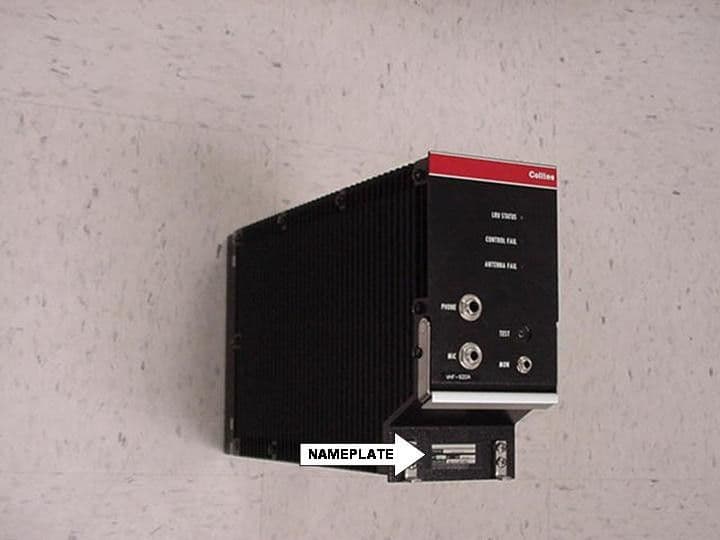
Click to zoom
Application Details
- Equipment Class
- TNB - Licensed Non-Broadcast Station Transmitter
- Date of Grant
- Apr 30, 2006
- Application Purpose
- Original Equipment
- Date of Application
- Feb 12, 2006
- Equipment Note
- VHF-2100E Extended Range Transceiver
- Frequency Range
- 118.00000000 - 150.80000000
- Company
- Rockwell Collins Inc
- Country
- United States
Documents & Files
Document Text
Text extracted from the exhibit documents filed with the FCC. Open a document above to read the original.
Users Manual
1. USER’S MANUAL – EXHIBIT H Rockwell Collins does not supply operating instructions with the VHF-2100E, which is designed to meet the requirements of of ARINC 716 and ARINC 750 and is operated by trained pilots as part of the VHF Communications system. Rockwell Collins does produce the VHF-2100/VHF-2100E Component Maintenance Manual, a comprehensive installation manual which, pursuant to an agreement with the FCC staff, is available upon request but is not included in this electronic exhibit.
Attestation Statements
ATTESTATION STATEMENT: The VHF-2100E has been tested in accordance with the requirements contained in the appropriate Commission regulations. To the best of my knowledge, these tests were performed using measurement procedures consistent with industry or Commission standards and demonstrate that the VHF-2100E complies with the appropriate standards. Each unit manufactured, imported, or marketed, as defined in the Commission’s regulations, will conform to the sample(s) tested within the variations that can be expected due to quantity production and testing on a statistical basis. I hereby certify that the tests described in this report were performed at my direction and under my supervision, and that the results and test data contained in this report truly and accurately show the performance of the transmitter in the VHF-2100E transceiver. I further certify that the ancillary information contained herein accurately reflects the design, installation requirements, alignment procedures, and operational instructions of and for this transceiver. Signed: Kenneth Hamby Hardware Engineer, VHF-2100E Melbourne Design Center Rockwell Collins, Inc.
Block Diagram
1.1.1 Functional Block Diagram LPF T/R Transmitter Receiver Frequency Synthesizer Frequency Synthesizer DAC & ADC / Control lines System Processor Maintenance Processor VOCODER I/O - ARINC, Discretes Rear ConnectorLED Card Antenna A1 RF CardA2 Digital/PS Power Supply A3 Rear Interconnect A4 LED Interface 1.1.2 Interface Diagram VHF-2100 CMU (Optional) OMS ANALOG ACARS (Optional) 118.023 118.065 DATA AUDIO OUT D ATA KEY DATA AU DIO IN LS 429 HS CMU HS PORT A V/D H S 429 FOR AU TOTUN E ANALOG MIC AUD IOPTT LS 429 OMS LS 429 OMS Next F requency U pload and Annunciations LS 429 PORT B LS TUNING CMU OUT CMU POR T A V/D POR T A LS TUNING PORT A OMS IN OMS OUT POR T A/B SELECT /2 /2 /2/2 +28 VD C OMS POR T B CMU POR T B TO OPPOSITE SID E CMU/OMS AUDIO SYSTEM V/D Enh V oic eVDL3 Data Activ e Preset Next AN TENN A 1.1.3 System Interconnect Diagram BZT Filter Rear Connector T/R SWITCH RECEIVER RX/TX SYN. RX_RF TX_RF TXRX_RF DSP/IO/MAINTENANCE/VOCODER IF_SIGNAL PRESEL_4 NEG_8VDC SCOM_TRESH POS_8VDC PRESEL_3 PRESEL_2 TRANS. RX_LO CLOCK DATA AGC_LEVEL TX_KEY TX_RF_ DRIVE RX_STROBE TX_STROBE REF_FREQ V-FWD V_REV Q_DET PRESEL_1 I_MOD Q_MOD Q_PHASE_ADJ PA_DRIVER_BIAS PA_FINAL_BIAS RX_SYNTH_LOCK TX_SYNTH_LOCK PA_TEMP POWER SUPPLY & CLAMP RF POS_15VDC PWR_WARN +28VDC_ MAIN_ BUSS VHF-2100 ASSEMBLY INTERFACE DIAGRAM A2 ASSEMBLY A1 ASSEMBLY CLAMP_ON_INT_F PS_FREQ DATA_INPUT_L KEY COAX RIBBON I_PHASE_ADJ MIC_INPUT_H AUDIO_OUT_H AUDIO_OUT_L ARINC 429 & Discretes POS_3.3VDC +28VDC_CLAMPED CHASSIS GND DATA_INPUT_H GND MIC_INPUT_L D8PSK_MODE MODE_3_CO_SITE FAST_AGC CLAMP_ENABLE T/R_SWITCH BIAS A3 ASSEMBLY RS- 232 LED's A4 ASSEMBLY (FRONT PANEL) DEBUG _PORT _RX DEBUG _PORT _TX GND Phone/ Mic MIC_GND S. T. FP_ KEYLINE FP_ SELF_ TEST CONTR _FAIL LRU_ PASS LRU_ FAIL ANT_ PASS ANT_ FAIL CONTR _PASS +28VDC_ MAIN_ BUSS 1.1.4 Transmitter Block Diagram PA ERROR AMPS/ LOOP FILTERS -40 dB cplr BTZ LP FILTER I-Q DEMOD I Q PHASE ADJUST TO RCVR INPUT PHASE_I PHASE_Q IQ LORF RF LO PHASE_I I_INPUT FWD_PWRREV_PWR PA TEMP +20 dBm RF Input PA TEMP SENSOR FWD/REV SENSORS Q_INPUT -30 dB Coupler T/R I-Q MOD 1.1.5 Receiver Block Diagram PS#1PS#2PS#3PS#4 RF AMP FM BAND REJECT MIX SIMULCOM ATTN SIMULCOM ATTN IF AMP MIX 28.900 MHz Crystal Filter +16 kHz BW 2 Pole Filter 2 Pole Filter 2nd Harmonic Rej Lo Input 146-165 MHz 17 dBm min Simulcomm Control output Simulcomm Detector/ Loop Amp RF Input (from T/R Switch) Simulcomm Control AGC Control 28.900 MHz IF output -20 dB COUPLER RF AMP and VHF BP FILTER AM Detector and 10.5 KHz Filter Integrator/ Comparator/ Monostable Mode 3 Co-Site Detect 1.1.6 Transmit Synthesizer Block Diagram 1.1.6.1 Detail of Regenerative Frequency Divider LPF - image rejection Amp BPF (Series LC) Mixer Pwr Splitter L R IF Reference Divider Phase/ Frequency detector Programmable divide by N Prescaler Loop Filter/ LPF VCO Regenerative Divide by 2 23.1 MHz TCXO (on A2 assy) Hi Isolation Amp 236-274 MHz +20 dBm 118-137 MHz Synthesizer Programming Data Output Enable 1.1.7 Receiver Synthesizer Block Diagram . 1.1.8 A2 DSP Circuit Card Block Diagram Reference Divider Phase/Frequency Detector Programmable Divide by N Counter 23.1 MHz TCXO - on A2 Assembly Dual-Modulus Prescaler VCO +17 dBm Min 146.900-166.000 MHz Loop Filter/LPF Reverse Isolation Amplifier Synthesizer Programming Data A/D Converter AD6640 bandpass sample Multirate Decimator/ Parallel- Serial AD6620 TMS320VC5416 DSP SYSP Intel 28F160C Flash 1M x 16 Snoopy 2 AD8801 8 output D/A Level Translators & Filters MAX146A/D x2 VHF IF 28.900 MHz Sport0 Rx Sport2 TX Sport2 Rx Sport1 Tx Level Translators & Filters ARINC-429 HS/LS Tx 1-8 ARINC-429 HS/LS Rx 1-16 Discrete Outputs A/D Bus Mic Audio H Data Audio In H V_FWD I Channel Tx Q Channel Tx RX Audio L RX Audio H AD5322 D/A RX Preselect I Mod I_Phase_ADJ Q_Phase_ADJ Data Audio Out H WD Tim er EPLD Glue Logic Discrete Inputs External Discrete Inputs: PTT Data Key SDI 1 SDI 2 CDFS_1_select CFDS_2_select Port B/A Select Tx Tim er D is able Voice/Data_Select Frequency of f set enable Data_load Shop_mode Squelch Disable Air-Ground Self test V_REF Tx_Synth Clock and Data Rx_Synth Clock and Data DSP +28 Vdc Spare 23.1 MHz Data Audio Out L Mo d e 3 De t e c t Rx Synth Lock Tx Synth Lock 80C188C MAINTP (VHF-920 reuse) TMS320VC5416 DSP VOCODER Sport0 Tx Sport0 Rx Sport0 TX Sport1 Rx WD WD WD 32.0 MH z RS-232 f ront panel External Discrete Outputs: Audio Mute Ela n d Serial 600 baud ARINC-429 OMS RX/ TX ARINC-429 OMS RX External AD5322 D/A X2 Q Mod Data Audio In L Mic Audio L Q Det AGC lev el
Cover Letter(s)
Exhibit List for VHF-2100E Extended Range Transceiver Exhibit A- Attestation Statement Exhibit B- FCC ID Label/Nameplate Exhibit C- External Photos Exhibit D- Block Diagrams Exhibit E- Schematic Diagrams Exhibit F- Test Report Exhibit G- Test Setup Photos Exhibit H- User’s Manual Exhibit I- Internal Photos Exhibit J- Tune-Up Procedure Parts List Exhibit K- RF Exposure Exhibit L – Operational Description Exhibit M- Capability Statement
External Photos
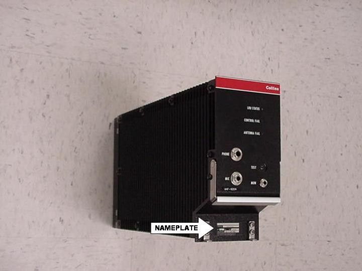
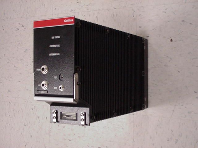
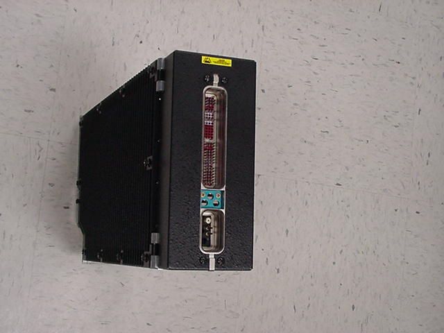
1. EQUIPMENT PHOTOGRAPHS – EXHIBIT C 1.1 VHF-2100E EXTERNAL VIEWS Index of Photographs Photo # Description ExtLeftCl.jpg Transceiver left with cover in place. ExtRtCl.jpg Transceiver right with cover in place. ExtRear.jpg Transceiver rear view showing ARINC connector.
ID Label/Location Info
1. NAMEPLATE LABEL DRAWING – EXHIBIT A The nameplate appears on the front of the transceiver. Its location is identified in the photographs and the drawing 983-8590-003 included in this Exhibit. Note that FCC Identifier and FAA TSO Approval Information is not shown on the product prior to approval by regulatory agencies. A copy of the final nameplate drawing is included with this exhibit.
Internal Photos
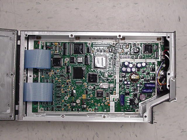
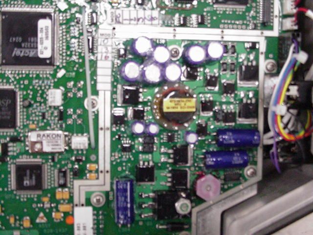
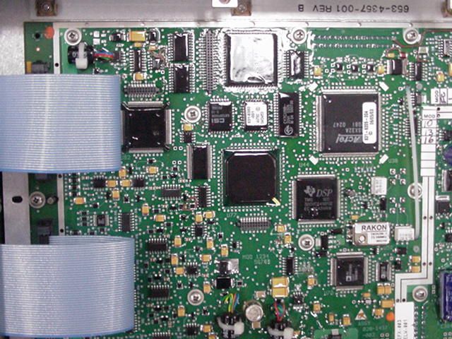
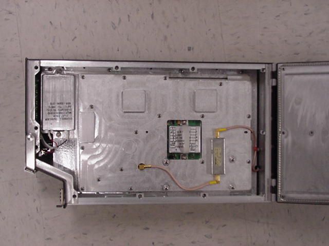
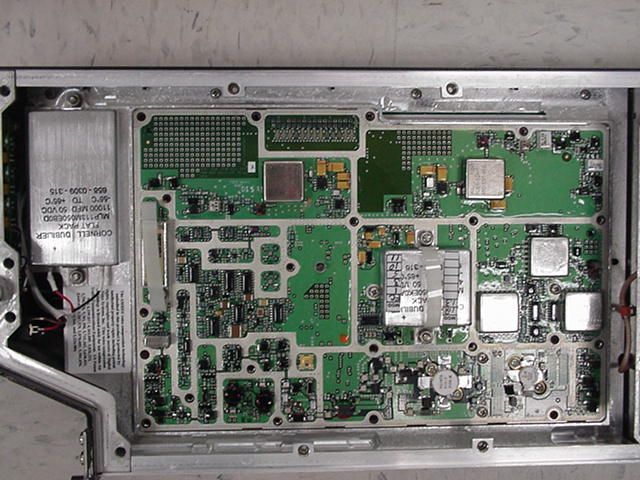
1. EQUIPMENT PHOTOGRAPHS – EXHIBIT I 1.1 VHF-2100E INTERNAL VIEWS Index of Photographs Photo # Description A2Over.jpg Transceiver from the front, left cover open showing A2 Power Supply/DSP Circuit Card Assembly. The power supply playthrough capacitor is shown on the A1 side. A2-PS.jpg Close up of Power Supply on the A2 CCA. A2-DSP.jpg Close up of A2 Digital Signal Processor CCA. A1Over.jpg Transceiver right side with cover open showing A1 RF Circuit Card Assembly cover. The component connected via coaxial cables is a Low Pass Filter. The large component with a plastic band visible over it is a storage capacitor for the VHF Power Amplifier. A1-Card.jpg Transceiver right side with close up of A1 VHF RF Assembly with cover removed, showing RF CCA and playthrough capacitor.
Operational Description
1.1 OPERATIONAL DESCRIPTION Major circuit schematics are attached to this report as Exhibit E. 1.1.1 GENERAL DESCRIPTION OF CIRCUITRY The VHF-2100E consists of 4 sub-assemblies; VHF RF Assembly, Digital/Power Supply Assembly, Rear Interconnect Assembly, and Front Panel LED Assembly. The VHF-2100E power amplifier linearly amplifies the transmitter synthesizer output to a 25 watt (minimum) carrier power level for AM voice or analog data operation. The power output in VDL Mode 2 is a minimum of 18 Watts. Voice, analog data, or digital data is impressed on the input RF from the synthesizer in a closed feedback loop vector (I-Q) modulator system, used as a variable RF attenuator and phase modulator. A synchronous detector sampling the RF power output provides amplitude and phase (I-Q) feedback information to the vector modulator to linearize the amplitude and phase characteristics of the power amplifier. A low pass filter at the output attenuates the transmitter harmonics further. The worst case harmonic found during testing was 76 dB below the carrier level. The VHF-2100E receiver utilizes a single conversion design. The receiver synthesizer injection is applied to the first mixer, generating a 28.900 MHz first IF frequency (high side injection) which is amplified and then detected by use of Digital Signal Processing technology. For voice operation, a noise quieting squelch and carrier squelch, both implemented in DSP, are provided. In data modes, no audio is presented to the operators. For receive operation, the VHF-2100E frequency synthesizer is a single loop, TXCO reference controlled design and provides the receive LO for any 25 kHz or 8.33 kHz channel selected in the 118.000 to 152.000 MHz frequency range. A second, dedicated frequency synthesizer is used for transmit operation. It is a single loop, TXCO reference controlled design and provides the direct transmit frequency RF drive for any 25 kHz or 8.33 kHz channel selected in the 118.000 to 152 MHz frequency range to the vector modulator and RF power amplifier. Both receive and transmit frequency synthesizers use a common 23.1 MHz +/- 5 PPM temperature compensated crystal oscillator (TCXO) as the reference. Both synthesizers use advanced DSP technology, sigma-delta modulated fractional-N synthesis, to improve spurious performance and reduce phase noise while providing small channel spacing. 1.1.2 NECESSARY BANDWIDTH CALCULATIONS Because of the high linearity of the VHF-2100E transmitter, the required bandwidth for transmissions follows the mathematical rules for the mode of communications in use. For DSB AM transmissions, the bandwidth for 99% power is twice the modulating frequency. Two modes of AM are used, 5K00A3E and 10K0A3D. In both cases, the 99% power bandwidth is twice the modulating frequency. The tests are performed with a modulating frequency of 2.5 kHz, yielding an occupied bandwidth of 5 kHz. In DO-281 and DO-271 data modes, 14K0G1DE and 14K0G7WET, system MOPS describes a power profile both in channel and in adjacent channels. The VHF-2100E out-performs the MOPS by typically 6 dB, and often as much as 10 dB. 1.1.3 CIRCUITRY FOR SUPPRESSION OF SPURIOUS RADIATION The low-pass filter suppresses transmitter spurious radiator. This is located on the RF Assembly and shown on schematic 828-1436-002. An additional low pass filter, common to both transmit and receive functions is in the common antenna cable from the unit. This filter provides additional filtering for transmitter harmonics in the 1.5 GHz GPS band. Non-harmonic spurious radiation is reduced by the advanced design of the phase locked loop frequency synthesizers and careful circuit board design. 1.1.4 CIRCUITRY FOR LIMITING MODULATION Modulation limiting is achieved in the audio compressor that is implemented in software on the Signal Processor. As the compressor characteristic curves in this report show, this compressor circuit operates as a linear amplifier until the input signal reaches such level that the software begins to reduce the gain by mathematically scaling the internal digitally processed signal. The large dynamic range above the compression knee minimizes the possibility of over-modulation. This guarantees that the RF output cannot go to zero, even during severe overdrive of the audio input to the compressor. 1.1.5 CIRCUITRY FOR LIMITING POWER The carrier power output is controlled by adjusting the DC component of the audio signal applied to the modulator controller, U800 on the RF assembly, 828-1436-002. This DC level is a service adjustment, not accessible to the operator. A software controlled reduction of peak power occurs during times of low power supply voltage (less than 22.0 VDC) to prevent distortion of the positive modulation peaks. This is also a service adjustment and not accessible to the operator. Separate modulation adjustments are provided for 25 KHz channel and 8.33 KHz channel operation. The 25 KHz channel and 8.33 channel modulation levels are set in software by values written into non-volatile memory. This is a service adjustment and not accessible to the operator. 1.2 DIGITAL MODULATION TECHNIQUES The Modulation format of the VHF-2100E Mode 2 is emission designator 14K0G1DE and 14K0G7WET for Mode 3. These are digital 31.5 kB/sec (10.5 kSym/sec) D8PSK waveforms using raised cosine shaping with excess bandwidth factor of 0.6. The modulation waveform is generated in software by a Digital Signal Processor in complex form (I,Q) with 12 bit precision. 12 bit resolution D/A converter outputs at an 84 k/sample rate is filtered by a 2 section linear phase type low pass filter with –3 dB cutoff frequency of 8.5 kHz. The amplitude and phase response of the low pass filters is shown in Table 1. Table 1 Frequency (Hz) Amplitude (dBr) Phase (Degrees) 100 0 -32 1000 0 -35 2000 -0.2 -40 3000 -0.3 -43 4000 -0.5 -46 5000 -1.5 -48 8500 -3 -50 10000 -4 -55 20000 -10 -70 100000 -30 -80 The filtered I, Q outputs are applied to a Vector (I,Q) modulator wh…
Text truncated - open the document above for the full version.
Test Report
FCC Certification Tests for the VHF-2100E Communications Transceiver CPN: 815-9528-001 9/16/2005 Page: 1 Exhibit F – Test Report TABLE OF CONTENTS EXHIBIT F – TEST REPORT .......................................................................................... 1 TABLE OF CONTENTS.................................................................................................. 1 1. TRANSMITTER PERFORMANCE TESTS – EXHIBIT I ........................................ 3 1.1 RF POWER OUTPUT .................................................................................................................... 3 1.1.1 REQUIREMENTS ...................................................................................................................3 1.1.2 TEST PROCEDURE............................................................................................................... 4 1.1.3 TEST RESULTS...................................................................................................................... 4 1.1.4 POWER OUTPUT DATA SHEET ........................................................................................... 5 1.1.5 RF LOAD CHARACTERISTICS.............................................................................................. 6 1.1.6 SMITH CHARTS ..................................................................................................................... 7 1.2 MODULATION CHARACTERISTICS............................................................................................ 8 1.2.1 REQUIREMENTS ...................................................................................................................8 1.2.2 TEST PROCEDURE............................................................................................................... 8 1.2.3 TEST RESULTS...................................................................................................................... 9 1.3 OCCUPIED BANDWIDTH ........................................................................................................... 15 1.3.1 REQUIREMENTS ................................................................................................................. 15 1.3.2 TESTS FOR TYPE 5K00A3E EMISSIONS .......................................................................... 16 1.3.3 TESTS FOR TYPE 10K0A3D EMISSIONS .......................................................................... 21 1.3.4 TESTS FOR TYPE 14K0G1DE EMISSIONS ....................................................................... 23 1.3.5 TESTS FOR TYPE 14K0G7WET EMISSIONS .................................................................... 24 1.4 SPURIOUS EMISSIONS AT ANTENNA TERMINAL................................................................. 25 1.4.1 REQUIREMENTS ................................................................................................................. 25 1.4.2 TEST PROCEDURE............................................................................................................. 26 1.4.3 TEST RESULTS....................................................................................................................26 1.5 FIELD STRENGTH OF SPURIOUS RADIATION ....................................................................... 30 1.5.1 REQUIREMENTS ................................................................................................................. 30 1.5.2 TEST PROCEDURE............................................................................................................. 31 1.5.3 TEST RESULTS....................................................................................................................31 FCC Certification Tests for the VHF-2100E Communications Transceiver CPN: 815-9528-001 9/16/2005 Page: 2 1.6 FREQUENCY STABILITY ........................................................................................................... 32 1.6.1 REQUIREMENTS ................................................................................................................. 32 1.6.2 TEST PROCEDURE............................................................................................................. 33 1.6.3 TEST RESULTS....................................................................................................................34 FCC Certification Tests for the VHF-2100E Communications Transceiver CPN: 815-9528-001 9/16/2005 Page: 3 1. TRANSMITTER PERFORMANCE TESTS – EXHIBIT I This section documents the test procedures used, and records the results of tests to demonstrate compliance with the applicable requirements of parts 2 and 87 of the FCC Rules and Regulations. 1.1 RF POWER OUTPUT 1.1.1 REQUIREMENTS FCC Sec. 2.1046 Measurements required: RF power output. (a) For transmitters other than single sideband, independent sideband and controlled carrier radiotelephone, power output shall be measured at the RF output terminals when the transmitter is adjusted in accordance with the tune-up procedure to give the values of current and voltage on the circuit elements specified in Sec. 2.1033(c)(8). The electrical characteristics of the radio frequency load attached to the output terminals when this test is made shall be stated. FCC 87.131 Power must be determined by direct measurement. The following lists authorized emissions and maximum power. Class of Station Frequency Band Emissions Power Aircraft (Communications) VHF A3E, A9W 55 w The power is measured at the transmitter output terminals and the type of power is determined according to the emission designator as follows: Mean power (pY) for amplitude modulated emissions and transmitting both sidebands using unmodulated full carrier. Power is restricted to the minimum necessary to achieve the required service. FCC Certification Tests for the VHF-2100E Communications Transceiver CPN: 815-9528-001 9/16/2005 Page: 4 1.1.2 TEST PROCEDURE The VHF-2100 was adjusted in accordance with the tune-up inst…
Text truncated - open the document above for the full version.
Test Report
FCC Certification Tests for the VHF-2100E Communications Transceiver CPN: 815-9528-001 9/16/2005 Page: 1 Exhibit F – Test Report TABLE OF CONTENTS EXHIBIT F – TEST REPORT .......................................................................................... 1 TABLE OF CONTENTS.................................................................................................. 1 1. TRANSMITTER PERFORMANCE TESTS – EXHIBIT I ........................................ 3 1.1 RF POWER OUTPUT .................................................................................................................... 3 1.1.1 REQUIREMENTS ...................................................................................................................3 1.1.2 TEST PROCEDURE............................................................................................................... 4 1.1.3 TEST RESULTS...................................................................................................................... 4 1.1.4 POWER OUTPUT DATA SHEET ........................................................................................... 5 1.1.5 RF LOAD CHARACTERISTICS.............................................................................................. 6 1.1.6 SMITH CHARTS ..................................................................................................................... 7 1.2 MODULATION CHARACTERISTICS............................................................................................ 8 1.2.1 REQUIREMENTS ...................................................................................................................8 1.2.2 TEST PROCEDURE............................................................................................................... 8 1.2.3 TEST RESULTS...................................................................................................................... 9 1.3 OCCUPIED BANDWIDTH ........................................................................................................... 15 1.3.1 REQUIREMENTS ................................................................................................................. 15 1.3.2 TESTS FOR TYPE 5K00A3E EMISSIONS .......................................................................... 16 1.3.3 TESTS FOR TYPE 10K0A3D EMISSIONS .......................................................................... 21 1.3.4 TESTS FOR TYPE 14K0G1DE EMISSIONS ....................................................................... 23 1.3.5 TESTS FOR TYPE 14K0G7WET EMISSIONS .................................................................... 24 1.4 SPURIOUS EMISSIONS AT ANTENNA TERMINAL................................................................. 25 1.4.1 REQUIREMENTS ................................................................................................................. 25 1.4.2 TEST PROCEDURE............................................................................................................. 26 1.4.3 TEST RESULTS....................................................................................................................26 1.5 FIELD STRENGTH OF SPURIOUS RADIATION ....................................................................... 30 1.5.1 REQUIREMENTS ................................................................................................................. 30 1.5.2 TEST PROCEDURE............................................................................................................. 31 1.5.3 TEST RESULTS....................................................................................................................31 FCC Certification Tests for the VHF-2100E Communications Transceiver CPN: 815-9528-001 9/16/2005 Page: 2 1.6 FREQUENCY STABILITY ........................................................................................................... 32 1.6.1 REQUIREMENTS ................................................................................................................. 32 1.6.2 TEST PROCEDURE............................................................................................................. 33 1.6.3 TEST RESULTS....................................................................................................................34 FCC Certification Tests for the VHF-2100E Communications Transceiver CPN: 815-9528-001 9/16/2005 Page: 3 1. TRANSMITTER PERFORMANCE TESTS – EXHIBIT I This section documents the test procedures used, and records the results of tests to demonstrate compliance with the applicable requirements of parts 2 and 87 of the FCC Rules and Regulations. 1.1 RF POWER OUTPUT 1.1.1 REQUIREMENTS FCC Sec. 2.1046 Measurements required: RF power output. (a) For transmitters other than single sideband, independent sideband and controlled carrier radiotelephone, power output shall be measured at the RF output terminals when the transmitter is adjusted in accordance with the tune-up procedure to give the values of current and voltage on the circuit elements specified in Sec. 2.1033(c)(8). The electrical characteristics of the radio frequency load attached to the output terminals when this test is made shall be stated. FCC 87.131 Power must be determined by direct measurement. The following lists authorized emissions and maximum power. Class of Station Frequency Band Emissions Power Aircraft (Communications) VHF A3E, A9W 55 w The power is measured at the transmitter output terminals and the type of power is determined according to the emission designator as follows: Mean power (pY) for amplitude modulated emissions and transmitting both sidebands using unmodulated full carrier. Power is restricted to the minimum necessary to achieve the required service. FCC Certification Tests for the VHF-2100E Communications Transceiver CPN: 815-9528-001 9/16/2005 Page: 4 1.1.2 TEST PROCEDURE The VHF-2100 was adjusted in accordance with the tune-up inst…
Text truncated - open the document above for the full version.
Contact Information
Applicant
Thomas A. Voltero(Director & Senior Counsel)
Technical Contact
Rockwell Collins, Inc.John M. Gifft
[email protected]7035168213
1300 Wilson Boulevard, Suite 200 · Arlington, Virginia · United States
Test Firm
Advanced Compliance Solutions, Inc.Sam Wismer
Technical Specifications
| # | Rule Parts | Frequency Range | Power Output | Emission | Tolerance |
|---|---|---|---|---|---|
| 3 | 87 | 118 MHz - 150.8 MHz | 20 W | 14K0D7D | 5 ppm |
Other Applications from Rockwell Collins Inc
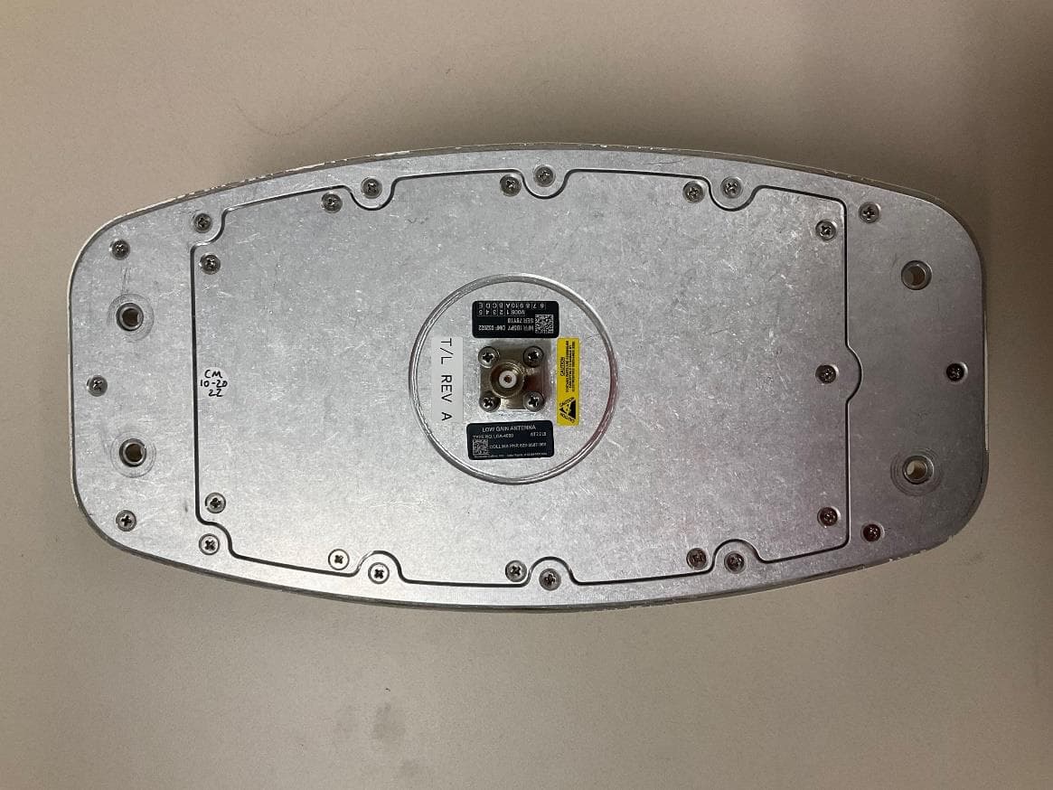
AJK8223587
Jan 23, 2023IRT-4200 SATCOM System
Equipment Class
TNB - Licensed Non-Broadcast Station Transmitter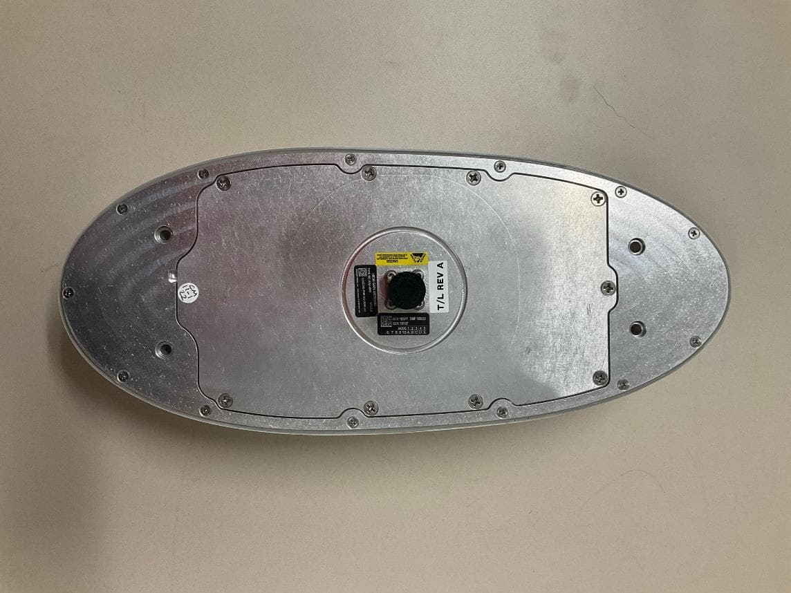
AJK8223586
Jan 23, 2023IRT-4400 SATCOM System
Equipment Class
TNB - Licensed Non-Broadcast Station Transmitter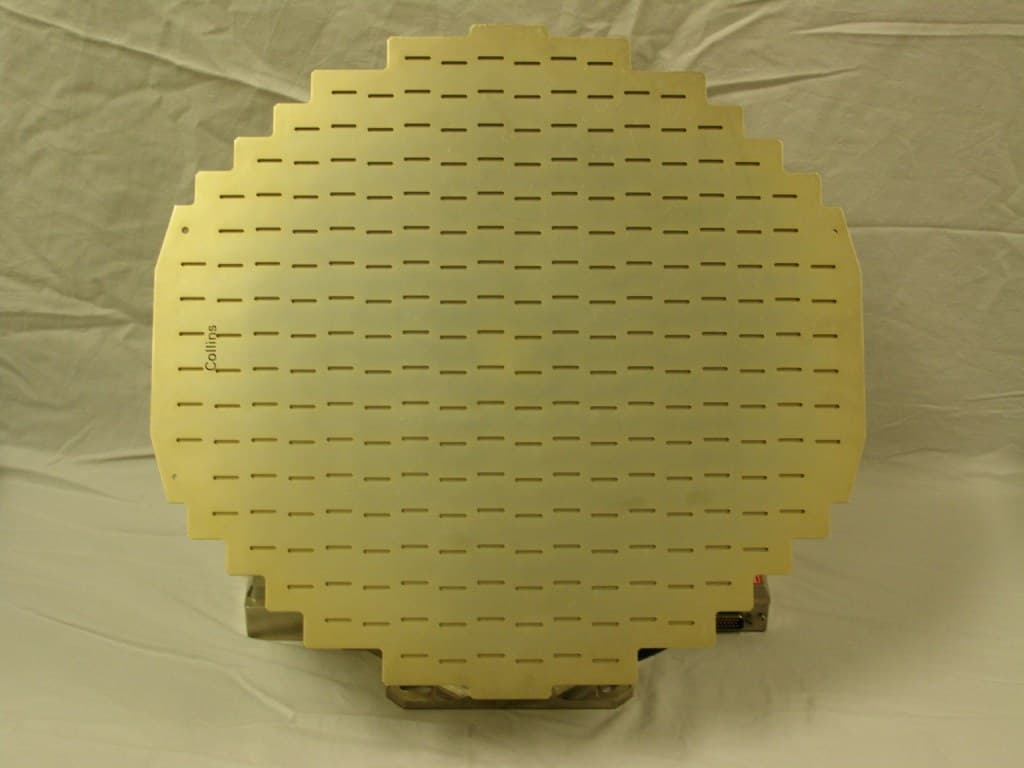
AJK8222259
Nov 11, 2015Weather Radar
Equipment Class
TNB - Licensed Non-Broadcast Station Transmitter
AJK8223132
May 20, 2015Information Management System
Equipment Class
DTS - Digital Transmission System
AJK8223075
Mar 04, 2013TCAS II Transmitter/Receiver
Equipment Class
TNB - Licensed Non-Broadcast Station Transmitter