AXATR-415-A2OEM Module
HARRIS CORPORATION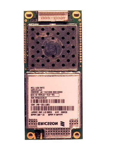
Click to zoom
Application Details
- Equipment Class
- TNB - Licensed Non-Broadcast Station Transmitter
- Date of Grant
- Sep 17, 2000
- Application Purpose
- Original Equipment
- Date of Application
- Aug 07, 2000
- Equipment Note
- OEM Module
- Frequency Range
- 824.00000000 - 849.00000000
- Company
- HARRIS CORPORATION
- Country
- United States
Documents & Files
Document Text
Text extracted from the exhibit documents filed with the FCC. Open a document above to read the original.
Users Manual
Exhibit 8: OEM Interface Manual ©2000 Ericsson Inc.Page 1 of 11 DM-10 OEM INTERFACE MANUAL Exhibit 8: OEM Interface Manual ©2000 Ericsson Inc.Page 2 of 11 CONTENTS – OEM INTERFACE MANUAL 1. DM10 TRANSCEIVER MODULE OUTLINE DRAWING.......................................................... 3 1.1.MECHANICAL.............................................................................................................................4 1.2.ELECTRICAL..............................................................................................................................5 1.2.1.ELECTRICAL PERFORMANCE...............................................................................................5 1.2.2.MOBILE STATION POWER CLASS.........................................................................................6 1.3.POWER CONSUMPTION..............................................................................................................6 1.3.1.TRANSMIT/TALK MODE......................................................................................................6 1.3.2.STANDBY MODE.................................................................................................................6 1.3.3.SLEEP MODE (MINIMUM DC POWER CONSUMPTION)..........................................................6 2. ABSOLUTE MAXIMUM RATINGS ............................................................................................. 7 3. SAFETY .......................................................................................................................................... 8 3.1.EXPOSURE TO RADIO FREQUENCY ENERGY.............................................................................8 3.2.MODULE OPERATION................................................................................................................8 3.3.POSTED FACILITIES...................................................................................................................8 3.4.ELECTRONIC DEVICES...............................................................................................................8 3.5.BLASTING AREAS.......................................................................................................................9 3.6.POTENTIALLY EXPLOSIVE ATMOSPHERES...............................................................................9 3.7.VEHICLES...................................................................................................................................9 3.8.FOR VEHICLES EQUIPPED WITH AN AIRBAG..............................................................................9 3.9.RESPONSIBLE USE.....................................................................................................................9 Exhibit 8: OEM Interface Manual ©2000 Ericsson Inc.Page 3 of 11 1. DM10 Transceiver Module Outline Drawing Exhibit 8: OEM Interface Manual ©2000 Ericsson Inc.Page 4 of 11 1.1. Mechanical The DM-10 module has no mechanical elements other that the main PCB assembly. All critical electronic components are shielded using sheet metal cans to prevent internal/external electromagnetic interference from degrading the module’s performance and to prevent the module from interfering with other nearby devices. The following figure shows a typical mounting configuration of the module with the main motherboard assembly. The module is plugged into the fixed mating connector and secured with four screws to the standoff components. Exhibit 8: OEM Interface Manual ©2000 Ericsson Inc.Page 5 of 11 1.2. Electrical The diagram below shows an overview of the electrical interface between the DM-10 module and a typical application. DM-10 Electrical Interface Customer Application HW Voltage Regulator Control Processor Voice & Data Processing üEcho Cancelling üNoise Cancelling üAudio Power AMP ü Data Conversion DTE Power External Audio Interface Antenna User Interface 6 1 Power & GND Serial Interface Wake Analog Audio Interface 10 1 3 5 4 Clock REF Option SIM Device DM-10 Module PCM Audio Interface 1.2.1. Electrical Performance Electrical performance parameters are valid only when the terminating impedance at the output of the antenna connector exhibits a VSWR of less than 2:1 for all phase angles in the frequency band of operation. High VSWR loads at the antenna connector adversely affect current consumption, linearity, and power efficiency of the module and may prevent operation or cause internal damage. The RF performance of the DM-10 fully meets the following specifications: • IS-136 TDMA Cellular mode – Per IS-137 specification • 553 AMPS Cellular mode – Per IS-19 specification Exhibit 8: OEM Interface Manual ©2000 Ericsson Inc.Page 6 of 11 1.2.2. Mobile Station Power Class The module is a power class IV unit for dual mode operation. The table below shows the nominal output power levels (Effective Radiated Power, assuming an antenna system gain of 1 dBd (3.15 dBi) [2.5 dBd (4.65 dBi) antenna gain with 1.5 dB cable loss)). Mobile Station Nominal Power Levels Mobile Station Power Level (dBW) 012345678910 Class IV-2-2-2-6-10-14-18-22 -27±3-32±4-37±5 *Note:Output power levels maintained within range of +2 / -4 dB unless otherwise noted. Power levels 8-10 valid for digital mode only. 1.3. Power Consumption 1.3.1. Transmit/Talk Mode DC current in mAAMPS ModeIS-136 ModeCDPD Mode Peak617590590Highest Power Level RMS617355355 1.3.2. Standby Mode DC current in mAAMPS ModeIS-136 ModeCDPD Mode RMS361515 1.3.3. Sleep Mode (Minimum DC Power consumption) A power down or "sleep mode" is available in which the module is placed in a low power consumption state under control of the host application. In this mode, the unit consumes approximately 33 uA of current as measured from the VCC_6V supply input on pin 1 of the system connector. A logic level "0" on pin 19 of the system connector returns the unit to full operation although there may be a significant delay while the module reestablishes registrat…
Text truncated - open the document above for the full version.
Users Manual
Exhibit 8: OEM Interface Manual ©2000 Ericsson Inc.Page 1 of 12 DM-10 OEM INTERFACE MANUAL Exhibit 8: OEM Interface Manual ©2000 Ericsson Inc.Page 2 of 12 CONTENTS – OEM INTERFACE MANUAL 1. DM10 TRANSCEIVER MODULE OUTLINE DRAWING.......................................................... 3 1.1.MECHANICAL.............................................................................................................................4 1.2.ELECTRICAL..............................................................................................................................5 1.2.1.ELECTRICAL PERFORMANCE...............................................................................................5 1.2.2.MOBILE STATION POWER CLASS.........................................................................................6 1.3.POWER CONSUMPTION..............................................................................................................6 1.3.1.TRANSMIT/TALK MODE......................................................................................................6 1.3.2.STANDBY MODE.................................................................................................................6 1.3.3.SLEEP MODE (MINIMUM DC POWER CONSUMPTION)..........................................................6 2. ABSOLUTE MAXIMUM RATINGS ............................................................................................. 7 3. SAFETY .......................................................................................................................................... 8 3.1.EXPOSURE TO RADIO FREQUENCY ENERGY.............................................................................8 3.2.MODULE OPERATION................................................................................................................8 3.3.POSTED FACILITIES...................................................................................................................8 3.4.ELECTRONIC DEVICES...............................................................................................................8 3.5.BLASTING AREAS.......................................................................................................................9 3.6.POTENTIALLY EXPLOSIVE ATMOSPHERES...............................................................................9 3.7.VEHICLES...................................................................................................................................9 3.8.FOR VEHICLES EQUIPPED WITH AN AIRBAG..............................................................................9 3.9.RESPONSIBLE USE.....................................................................................................................9 Exhibit 8: OEM Interface Manual ©2000 Ericsson Inc.Page 3 of 12 1. DM10 Transceiver Module Outline Drawing Exhibit 8: OEM Interface Manual ©2000 Ericsson Inc.Page 4 of 12 1.1. Mechanical The DM-10 module has no mechanical elements other that the main PCB assembly. All critical electronic components are shielded using sheet metal cans to prevent internal/external electromagnetic interference from degrading the module’s performance and to prevent the module from interfering with other nearby devices. The following figure shows a typical mounting configuration of the module with the main motherboard assembly. The module is plugged into the fixed mating connector and secured with four screws to the standoff components. Exhibit 8: OEM Interface Manual ©2000 Ericsson Inc.Page 5 of 12 1.2. Electrical The diagram below shows an overview of the electrical interface between the DM-10 module and a typical application. DM-10 Electrical Interface Customer Application HW Voltage Regulator Control Processor Voice & Data Processing üEcho Cancelling üNoise Cancelling üAudio Power AMP ü Data Conversion DTE Power External Audio Interface Antenna User Interface 6 1 Power & GND Serial Interface Wake Analog Audio Interface 10 1 3 5 4 Clock REF Option SIM Device DM-10 Module PCM Audio Interface 1.2.1. Electrical Performance Electrical performance parameters are valid only when the terminating impedance at the output of the antenna connector exhibits a VSWR of less than 2:1 for all phase angles in the frequency band of operation. High VSWR loads at the antenna connector adversely affect current consumption, linearity, and power efficiency of the module and may prevent operation or cause internal damage. The RF performance of the DM-10 fully meets the following specifications: • IS-136 TDMA Cellular mode – Per IS-137 specification • 553 AMPS Cellular mode – Per IS-19 specification Exhibit 8: OEM Interface Manual ©2000 Ericsson Inc.Page 6 of 12 1.2.2. Mobile Station Power Class The module is a power class IV unit for dual mode operation. The table below shows the nominal output power levels (Effective Radiated Power, assuming an antenna system gain of 1 dBd (3.15 dBi) [2.5 dBd (4.65 dBi) antenna gain with 1.5 dB cable loss)). Mobile Station Nominal Power Levels Mobile Station Power Level (dBW) 012345678910 Class IV-2-2-2-6-10-14-18-22 -27±3-32±4-37±5 *Note:Output power levels maintained within range of +2 / -4 dB unless otherwise noted. Power levels 8-10 valid for digital mode only. 1.3. Power Consumption 1.3.1. Transmit/Talk Mode DC current in mAAMPS ModeIS-136 ModeCDPD Mode Peak617590590Highest Power Level RMS617355355 1.3.2. Standby Mode DC current in mAAMPS ModeIS-136 ModeCDPD Mode RMS361515 1.3.3. Sleep Mode (Minimum DC Power consumption) A power down or "sleep mode" is available in which the module is placed in a low power consumption state under control of the host application. In this mode, the unit consumes approximately 33 uA of current as measured from the VCC_6V supply input on pin 1 of the system connector. A logic level "0" on pin 19 of the system connector returns the unit to full operation although there may be a significant delay while the module reestablishes registrat…
Text truncated - open the document above for the full version.
Attestation Statements
APPLICANT: ERICSSON INC.FCC ID NO: AXATR-415-A2 Exhibit 2A ©2000 Ericsson Inc. Para. 22.919, Electronic Serial Numbers Protection Against Unauthorized ESN and Firmware Upgrades The Electronic Serial Number (ESN) bits in this OEM module are encoded and spread over various non-sequential memory locations in order to prevent detection and modification. Once the factory has programmed the ESN, the mobile firmware cannot overwrite or alter the ESN memory locations. Both the ESN host and the operation systems components are permanently mounted to the mobile in order to prevent removal and misuse. Unauthorized attempts to alter the mobile’s firmware will cause the unit to become inoperable. APPLICANT: ERICSSON INC.FCC ID NO: AXATR-415-A2 Exhibit 2B ©2000 Ericsson Inc.
Attestation Statements
APPLICANT: ERICSSON INC FCC ID NO: AXATR-415-A2 ©2000 Ericsson Inc. Exhibit 2 Index for Exhibit Exhibit #Description 2AProtection Against Unauthorized ESN and Firmware Upgrades 2BCertification of Data 2CCompliance Statement to Part 22.921, 911 Call Processing Procedures APPLICANT: ERICSSON INC FCC ID NO: AXATR-415-A2 ©2000 Ericsson Inc. Exhibit 2A Para. 22.919, Electronic Serial Numbers Protection Against Unauthorized ESN and Firmware Upgrades The Electronic Serial Number (ESN) bits in this OEM module are encoded and spread over various non-sequential memory locations in order to prevent detection and modification. Once the factory has programmed the ESN, the mobile firmware cannot overwrite or alter the ESN memory locations. Both the ESN host and the operation systems components are permanently mounted to the module in order to prevent removal and misuse. Unauthorized attempts to alter the mobile’s firmware will cause the unit to become inoperable. APPLICANT: ERICSSON INC FCC ID NO: AXATR-415-A2 ©2000 Ericsson Inc. Exhibit 2B APPLICANT: ERICSSON INC FCC ID NO: AXATR-415-A2 ©2000 Ericsson Inc. Exhibit 2C Compliance Statement Pursuant to CC Docket No. 94-102, Section 22.921 Ericsson certifies that it is in full compliance with Section 22.921 of the FCC's Rules. Ericsson has received approval for its call processing method and has incorporated required modifications rendering it fully compliant with 47 C.F.R. Section 22.921 of the FCC's Rules. (See DA 00-253 released February 11, 2000)
Cover Letter(s)
August 2, 2000 Federal Communications Commission Authorization & Evaluation Division 7435 Oakland Mills Road Columbia, Maryland 21406 Attention:Equipment Authorization Branch Subject:Certification for FCC ID: AXATR-415-A2 Gentlemen, Ericsson Inc. requests certification (type acceptance) for the AXATR-415-A2. This OEM module transceiver is designed as a mobile for use in the AMPS/DAMPS cellular telephone system operating in the 800 MHz Domestic Public Cellular Radiotelephone Communications Services per Subpart H of part 22. This OEM module meets the requirements of IS-137A for operation in cellular systems. This OEM module is similar to previously type accepted FCC ID: AXATR-400-A2. Ericsson requests an exclusion from routine RF exposure measurements based on the discussion presented in Exhibit 11, RF Exposure Evaluation, since the analysis of the maximum RF exposures under worst-case and typical conditions clearly demonstrates compliance with the amended FCC rules. We have included specific instructions and warnings in Exhibit 8, OEM Interface Manual, regarding minimum separation distance, maximum antenna gain, and that use as a portable transmitter will require separate FCC approval for SAR compliance. Ericsson Inc. requests confidentiality under 47 CFR 0.459 for the following exhibits listed: Exhibit 4Block Diagram Exhibit 5Schematic Diagrams Justification of this request is that in order to facilitate the circuit miniaturization of the AXATR-415-A2, proprietary techniques were implemented in the transmitter, receiver, and baseband circuitry. To protect Ericsson’s competitive advantage on these proprietary techniques, we request the above listed exhibits be held as confidential and withheld from the Public Information File. Sincerely, Jim Sponsler Staff Engineer, Regulatory ServicesTel No:(919) 472-6460 Research Triangle Park, NCFax No:(919) 472-7452 August 2, 2000 Federal Communications Commission Equipment Approval Services PO Box 358315 Pittsburgh, PA 15251-5315 Subject:Enclosed a check for Type Acceptance and Confidentiality follows: FCC IDFEE AXATR-415-A2$ 580.00 Sincerely, John Rothgeb Specialist Regulatory Programs Room 2669 Tel:(804) 592-7476 Fax:(804) 592-6510 Enclosures:Check Filing for Equipment Approval Branch
Cover Letter(s)
To:Frank Coperich [email protected] FCC Application Processing Branch From:Jim Sponsler, Ericsson Inc Re:FCC ID AXATR-415-A2 Applicant:Ericsson Inc Correspondence Reference Number:15904 731 Confirmation Number:EA98413 Date of Original E-Mail:09/05/2000 Ericsson, EA 98413 - 1. Filing has made a request for exclusion from routine MPE evaluation and also indicate that the current device is similar to a previously approved device (AXATR-400-A2, EA 94593). The current device is requesting for a maximum output of 355 mW for all operating modes, therefore, all modes should be categorically excluded from routine MPE if all outputs are less than 1.5 W ERP. The previous device had 3.0 W peak output for one of its modes, which was not categorically excluded from routine MPE evaluation and had requested for an exclusion. Please clarify the maximum output of all operating modes for the current device and its association with the previous device (has same model number, DM-10) described in the cover letter. The previously approved device (AXATR-400-A2) was renamed from a DM10 to a DM10A, with the “A” suffix indicating the presence of 3.0 W peak output burst mode amplifier circuitry. The current device being certified is known as the DM10, and it does not include the burst mode circuitry, and is limited in output power to 355 mW for all operating modes. 2. Exhibit 6G1 (Ericsson labeled) describes a DM-20 module, please clarify which modules are included in this filing. The reference to the DM20 is a typo, it should have read DM10. The amended (corrected) document is attached, Exhibit 6G Rev B. 3. Please modify proposed "Safety" Section of the manual to indicate in Section 3.1 that this OEM module is designed and must be configured to operate with respect to Section 2.1091 of FCC rules, as a mobile transmitting device for satisfying RF exposure compliance requirements. It is not intended for use in hand-held or portable transmitting devices, which are required to obtain separate FCC approval to satisfy SAR compliance with respect to 2.1093 of FCC rules. OEM integrators are cautioned to follow these requirements. Exhibit 8 has been modified to reflect the recommended changes, and is attached, Exhibit 8 Rev B. 4. FYI - RF exposure info (section 1.2) describes device has 355 mW ERP, which should be conducted output. Section 2.3 describes a 30 minute averaging time, which is only applicable to fixed-mounted transmitters. Mobile and portable transmitters are required to satisfy source-based time-averaging requirements; please review rules in 2.1091 and 2.1093. MPE limits are more restrictive at the low end of the frequency band, MPE should be estimated with limits at the lowest operating frequency for the device to ensure compliance. Exhibit 11 has been corrected, and is attached, Exhibit 11 Rev B. 5.) Please submit a showing of compliance with the E-911 requirements under Section 22.921 Exhibit 2 has been amended to address E-911, and is attached, Exhibit 2 Rev B. The items indicated above must be submitted before processing can continue on the above referenced application. Failure to provide the requested information within 60 days of the original e-mail date may result in application dismissal pursuant to Section 2.917 (c) and forfeiture of the filing fee pursuant to section 1.1108. DO NOT reply to this e-mail by using the Reply button. In order for your response to be processed expeditiously, you must upload your response via the Internet at www.fcc.gov, Electronic Filing, OET Equipment Authorization Electronic Filing. If the response is submitted through Add Attachments, in order to expedite processing, a message which informs the processing staff that a new exhibit has been submitted must also be submitted via Submit Correspondence. Also, please note that partial responses increase processing time and should not be submitted. Any questions about the content of this correspondence should be directed to the e-mail address listed below the name of the sender.
External Photos
APPLICANT: ERICSSON INC.FCC ID: AXATR-415-A2 ©2000 Ericsson Inc. Exhibit 3: External Photo (Front View)Page 1 of 2 APPLICANT: ERICSSON INC.FCC ID: AXATR-415-A2 ©2000 Ericsson Inc. Exhibit 3: External Photo (Back and Side Views)Page 2 of 2
ID Label/Location Info
APPLICANT: ERICSSON INC.FCC ID: AXATR-415-A2 Exhibit 1: Identification Plate ©2000 Ericsson Inc.
Internal Photos
APPLICANT: ERICSSON INC.FCC ID: AXATR-415-A2 Exhibit 9: Internal Photos (Front and Back) ©2000 Ericsson Inc.
Operational Description
APPLICANT: ERICSSON INCFCC ID NO: AXATR-415-A2 Exhibit 12APage 1 of 3 ©2000 Ericsson Inc. CIRCUIT & DEVICE DESCRIPTIONS PARA. 2.1033 (b)(4), (c)(10) (10)FREQUENCY STABILIZATION A temperature compensated crystal oscillator (N1402) provides a 19.44 MHz reference frequency signal for the transmitter and receiver frequency synthesizers. This reference frequency is internally compensated to be within ±2.5 ppm over the temperature range of -30°C to +75° C. Upon power-up, the receiver searches and acquires a base station signal, and it adjusts the reference oscillator frequency to align itself to the high accuracy time base of the base station. The transmitter does not engage until after the receiver synchronizes to the base station. (11a)ATTENUATION OF SPURIOUS EMISSIONS The 800 MHz band transmitter frequency is obtained from mixing a phase locked VCO operating from 979.53 MHz to 1004.49 MHz with a 155.52 MHz signal. The 155.52 MHz signal is obtained by phase locking an oscillator to the VCTCXO output. The 800 MHz band receiver frequency is obtained by dual conversion. The first conversion is obtained by mixing the incoming signal with the 979.53 MHz to 1004.49 MHz VCO to a first IF frequency of 110.52 MHz. The second conversion mixes the IF frequency with a phase locked VCO at 110.4 MHz to obtain the second IF frequency of 120 kHz. All VCO’s are phase locked to the reference VCTCXO. As a result of the above circuitry, the spurious signals are transmitter harmonics, reference oscillator 19.44 MHz harmonics, the local oscillators and the microprocessor clock. The use of multi-layer printed circuit boards, with signal tracks between ground planes, for the radio as well as for the logic areas reduces the radiation to a minimum. Ceramic resonator bandpass filters for the duplexer attenuate conducted transmitter harmonics, reference oscillator and local oscillator signals. A bandpass filter in the receiver front end attenuates the local oscillator signal further. Additional suppression of radiation is achieved by shielding and key isolation between circuits. (11b)LIMITING MODULATION The modulation for the transmitter is produced inside a Digital Signal Processing integrated circuit. The modulation limiting is therefore controlled by an algorithm inside this chip. The limit is preset at the factory and cannot be changed thereafter. ATTENUATING HIGHER AUDIO FREQUENCIES The DSP chip provides an audio filter with a 120 log (f/3000) response, f=3K to 20KHz. Manchester encoded data signals are filtered prior to transmission by a four-pole lowpass filter providing an attenuation of 24 dB/Octave above 20 kHz. The signal produced by the DSP chip is a differentially shifted PI/4 QPSK signal for the digital system and a FM signal for the analog cellular system. These signals are fed through a three-pole lowpass filter with a 3 dB down cut-off frequency of 25 kHz to limit the adjacent channel energy in the digital mode. APPLICANT: ERICSSON INCFCC ID NO: AXATR-415-A2 Exhibit 12APage 2 of 3 ©2000 Ericsson Inc. CIRCUIT & DEVICE DESCRIPTIONS PARA. 2.1033 (b)(4) (11c)OUTPUT POWER CONTROL A loop circuit under supervision of the logic sets the output to any of the eleven power levels. A digital word is transmitted to the gain control amplifier for output power adjustment. A detector at the output of the power amplifier module senses the RF energy present and sends a corresponding DC voltage to the digital logic circuitry. Upon receiving a command to set power level from the handset or from a base station the microprocessor sends a predetermined word to the ALC amplifier. The output detector voltage is then read by the microprocessor and compared to a preset value. If the detector voltage is outside the allowed tolerance an adjustment is made to the gain-controlled amplifier to bring the detector voltage into the proper range. (12)DIGITAL MODULATION TECHNIQUES The NRZ data stream is transformed to 10kbps Manchester encoded data in such a way that each NRZ binary one is transformed to a zero-to-one transition, and each NRZ binary zero is transformed to a one-to-zero transition. The Manchester encoded data stream is filtered before being applied to the modulator. Direct binary frequency shift keying is used. A binary one into the modulator corresponds to a normal peak frequency deviation of 8kHz above the carrier frequency and a zero corresponds to a nominal peak frequency deviation 8 kHz below the carrier frequency. (12a)DESCRIPTION OF PI/4 DQPSK The modulation method used for the digital mode is known as PI/4 shifted differentially encoded Quadrature Phase Shift Keying. Eight distinct phase states are possible. The signal information is differentially encoded; symbols are transmitted as changes in phase rather than absolute phases. Transition of phase which would result in a zero amplitude momentarily are not allowed. APPLICANT: ERICSSON INCFCC ID NO: AXATR-415-A2 Exhibit 12APage 3 of 3 ©2000 Ericsson Inc. CIRCUIT & DEVICE DESCRIPTIONS PARA. 2.1033 (b)(4) 1.0 LOGIC BOARD OPERATION The logic board is the central controller system for the radio. It is made up of a microprocessor, DSP, codec, memory, and control logic. 1.1 ASIC CONTROL CHIP – D401 The ASIC control chip is made up of a ARM microprocessor and application specific logic circuits. The chip is the main control center for the radio and provides interfaces to the DSP’s, codec, memories, keypad, display, alarms, and system interfaces. 1.2 MEMORY CHIP’S D501 is the 1M x 8 flash memory used to store the radio’s operating algorithm. This part may be field programmed to allow new revisions of the operating algorithm to be installed without opening the radio case. D502 is the 256k x 8 static RAM used for stack, and microprocessor operation. D503 is the 32k x 8 electrically erasable programmable read only memory. The part stores all of the users phone numbers, any system parameters that change, and the power down status of the radio. 1.3 USER INTERFACE There is a 30 p…
Text truncated - open the document above for the full version.
Parts List/Tune Up Info
APPLICANT: FCC ID NO: ERICSSON INC. AXATR-415-A2 ©2000 Ericsson Inc. EXHIBIT 10 Index 10 A Description of active devices 10 B Alignment/ tune- up procedure APPLICANT: ERICSSON INC. FCC ID NO: AXATR-415-A2 ©2000 Ericsson Inc. Exhibit 10A DESCRIPTION OF ACTIVE DEVICES COMPONENT DESIGNATION FUNCTION OF DEVICE TRANSMITTER N1701 Power Amplifier V1720 Detector Diode V1702 Switching Transistor Z1802 800 MHz Duplexer Filter Z1701 Isolator, 800 MHz Z1601 800 MHz Transmit SAW Filter RECEIVER N1202 LNA/Mixer ASIC N1301 Receiver IF IC V1301 Tuning Diode V1201, V1202 Switching Transistor Z1203 800 MHz SAW Filter Z1204 Crystal Filter SYNTHESIZER N1501 VCO Module N1401 Synthesizer/ Modulator IC N1402 19.44MHz Oscillator Module V1501 FET Amplifier V1401 Tuning Diode BASEBAND D201 Hex Inverter D501, D502, D503 Memory D601 Digital Signal Processor D701 Audio Processor D402 OR gate D401 Microprocessor N301 Voltage Regulator ASIC N601, N1901, N1902 N1904 Voltage Regulators V201, V202, V203, V702, V703, Diode Clippers V204, V205, V701, V1903, V1905 switching transistors V902, V903, V904, V1201, V1202 switching transistors V1904, V1906, V1907 Switching FET V905 diode APPLICANT: ERICSSON INC. FCC ID NO: AXATR-415-A2 Exhibit 10B ALIGNMENT PROCEDURE Page 1 of 4 ©2000 Ericsson Inc. PARA. 2.1033 (c)(9) Due to the high accuracy of the I/O, the modulation, transmit voice, DTMF, SAT and data deviations are all preset in the DSP software and are not adjustable in production or the field. These procedures give the test method to verify the phone has proper deviations. RADIO TUNE/TEST INSTRUCTIONS FILTERING SAW, ceramic, and crystal filter technologies are used, and no tuning is required. REFERENCE FREQUENCY ADJUSTMENT TEST SETUP Testing of the VCTCXO circuit is temperature dependent and should be carried out at an ambient room temperature of +23°C to +27°C. Any frequency adjustments should be made 1.0 hour after re-flow soldering to allow for relaxation of thermal stress. Terminate ANT (X1802) into a frequency counter with a 50Ω input impedance. Enter the following test commands: **** The same channel should be used for all parts of this test **** @2705 (read thermistor A/D from Patti) check result 1 @80 (initialize the transceiver- carrier off and audio muted) @6502 (AFC off) @E11401FF (center DAC3) @3Czzxxxx (select a MID-CHANNEL) @8407 (set the transmitter power level 7) @81 (turn the transmitter on) check result 2 TEST RESULTS 1. Verify that the returned value is in the range 41 to 54 hex. (A higher temperature corresponds to a lower reading). 2. Wait until output is stable (<±42Hz variation in frequency). Log output frequency and calculate error in Hz. Verify that the transmitter frequency is <±100Hz of the channel frequency. If necessary, adjust DAC3 with the commands @E1140xxx where xxx is 000 to 3FF (each step is approx. 48Hz) to achieve a transmitter frequency that is <±100Hz of the channel frequency plus 0.35ppm. DAC3 calibration limits are 110h and 300h. END OF TEST @80…
Text truncated - open the document above for the full version.
Contact Information
Applicant
Thomas Camper, Jr.(Regulatory Manager)
Technical Contact
Ericsson IncJim Sponsler
[email protected]919-472-6460
7001 Develpment Drive · Research Triangle Park, North Carolina · United States
Non-Technical Contact
Ericsson IncJim Sponsler
[email protected]919-472-6460
Technical Specifications
| # | Rule Parts | Frequency Range | Power Output | Emission | Tolerance |
|---|---|---|---|---|---|
| 3 | 22.901(d) | 824 MHz - 849 MHz | 355.00 mW | 30K0DXW | 2.5 ppm |
Other Applications from HARRIS CORPORATION

AXATR-423-A2
Jul 14, 2004CM-42
Equipment Class
PCB - PCS Licensed Transmitter
AXATR-420-A2
Mar 21, 2002DM-15
Equipment Class
TNB - Licensed Non-Broadcast Station Transmitter
AXATR-422-A2
Mar 13, 2002Dual Mode TDMA Cellular Handset
Equipment Class
TNE - Licensed Non-Broadcast Transmitter Held to Ear
AXATR-421-A2
Dec 19, 2001Dual Mode TDMA Cellular Transceiver
Equipment Class
TNE - Licensed Non-Broadcast Transmitter Held to EarAXATR-413-A2
Aug 14, 2001cellular/pcs portable terminal
Equipment Class
PCE - PCS Licensed Transmitter held to ear