B32RF350RFID Device
VeriFone Inc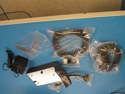
Click to zoom
Application Details
- Equipment Class
- DXX - Part 15 Low Power Communication Device Transmitter
- Date of Grant
- Jan 30, 2000
- Application Purpose
- Original Equipment
- Date of Application
- Oct 14, 1999
- Equipment Note
- RFID Device
- Frequency Range
- 13.56000000 - 13.56000000
- Company
- VeriFone Inc
- Country
- United States
Documents & Files
Document Text
Text extracted from the exhibit documents filed with the FCC. Open a document above to read the original.
Users Manual
VeriFone Indoor VeriPASS Terminal Installation Guide P/N: 55295 Revision A VeriFone Indoor VeriPASS Terminal Installation Guide August 15, 1999 VeriFone ® , a division of Hewlett-Packard 4988 Great America Parkway Santa Clara, CA 95054-1200 Telephone: 408-496-0444 http://www.verifone.com Printed in the United States of America. © 1999 by VeriFone, a division of Hewlett-Packard All rights reserved. No part of this publication covered by the copyrights herein may be reproduced or copied in any form or by any means — graphic, electronic, or mechanical, including photocopying, taping, or information storage and retrieval systems — without written permission of the publisher. The content of this document is subject to change without notice. The information contained herein does not represent a commitment on the part of VeriFone, a division of Hewlett-Packard. Publications are not stocked at the address given above. Requests for VeriFone publications should be made to your VeriFone representative. VeriFone is a registered trademark of Hewlett-Packard Company. All other products mentioned in this manual are trademarks or registered trademarks of their respective owners. VeriFone Indoor VeriPASS Terminal Installation Guide Revision History RevisionDateComments AAugust 15, 1999Initial release of software and documentation. FCC Compliance This equipment has been tested and found to comply with the limits for a Class B digital device, pursuant to Part 15 of the FCC Rules. These limits are designed to provide reasonable protection against harmful interference in a residential installation. This equipment generates, uses and can radiate radio frequency energy and, if not installed and used in accordance with the instructions, may cause harmful interference to radio communications. However, there is no guarantee that interference will not occur in a particular installation. If this equipment does cause harmful interference to radio or television reception, which can be determined by turning the equipment off and on, the user is encouraged to try to correct the interference by one or more of the following measures: n Reorient or relocate the receiving antenna. n Increase the separation between the equipment and receiver. n Connect the equipment into an outlet on a circuit different from that to which the receiver is connected. n Consult the dealer or an experienced radio/TV technician for help. Safety Instructions n Read all instructions contained in this guide before making any equipment connections. n Save these instructions for later use. n Unplug the unit before servicing or cleaning. Do not use liquid or aerosol cleaners. Use only a damp cloth for cleaning. n Do not use any attachments not specifically recommended by VeriFone as they may result in the risk of fire, electric shock, or injury to persons. n Do not use the unit near water. n Do not place the unit on an unstable cart, stand, or table. The unit may fall, causing serious personal injury and/or damage to the equipment. Contents u i Contents 1. Introduction . . . . . . . . . . . . . . . . . . . . . . . . . .1 2. Unpacking. . . . . . . . . . . . . . . . . . . . . . . . . . . .3 3. Installation . . . . . . . . . . . . . . . . . . . . . . . . . . .5 Installation Procedures . . . . . . . . . . . . . . . . . . . . . . . . . . . . . . . 5 Equipment Power Up . . . . . . . . . . . . . . . . . . . . . . . . . . . . . . . . 6 4. Specifications. . . . . . . . . . . . . . . . . . . . . . . . .9 Power Requirements . . . . . . . . . . . . . . . . . . . . . . . . . . . . . . . . 9 Operating Environment . . . . . . . . . . . . . . . . . . . . . . . . . . . . . . 9 Service and Repair . . . . . . . . . . . . . . . . . . . . . . . . . . . . . . . . . . 9 Cleaning . . . . . . . . . . . . . . . . . . . . . . . . . . . . . . . . . . . . . . . . . 10 ii u Contents Introduction u 1 1 Introduction This document provides the information necessary to install your VeriFone Indoor VeriPASS Terminal System. The VeriFone Indoor VeriPASS Terminal System is a self-contained device, when properly installed, becomes an integral part of the Ruby SuperSystem. It has the ability to read a retail customer’s tag when placed near an antenna mounted on the face of the equipment. Information from the tag is processed and transferred to the Ruby. nmobilind.wmf 125% Multicable Optional Power Supply* VeriFone Indoor Everest Base Unit Base Cable Ferrite Bead Cable Tie VeriPASS Terminal Installation Manual (VFI P/N: 04250-05) * Optional Power Supply not required when used with a Ruby SuperSystem 2 u Introduction Unpacking u 3 2 Unpacking Carefully inspect the shipping carton and its contents for any damage that may have occurred during shipment. If anything appears damaged, immediately file a claim with the shipping company or carrier and notify your VeriFone representative. Warning:Never use damaged equipment. A shock or fire hazard may exist if equipment is energized in a damaged condition. Remove the following items from the shipping carton: n VeriFone Indoor VeriPASS Terminal Unit with attached Mulitcable n Power Supply (optional) n Ferrite Bead Remove any protective plastic wrapping from the components and place the components on a table or countertop. Retain the shipping carton and any packing material in case it is necessary to move components from one location to another or to return the equipment for service. 4 u Unpacking Installation u 5 3 Installation Unpack equipment in accordance with instructions listed in Chapter 2. Warning:To reduce the risk of fire, do not place this unit near any heat producing source. When selecting a location for your VeriFone Indoor VeriPASS Terminal equipment, avoid areas having: n Direct sunlight or objects that produce heat. n Moist areas. n Excessive dust. n Electrical “noise” or devices that cause excessive voltage variations such as air conditioners, fans, or high frequency security systems. Installation Procedures Note:If not present, instal…
Text truncated - open the document above for the full version.
Cover Letter(s)
VeriFone 3755 Atherton Road Rocklin, CA 95765-3701 Tel: 916/630-0550 Fax: 916/630-2501 October 15, 1999 Federal Communications Commission Office of Engineering Technology Equipment Authorization Division Subject: Application for Equipment Authorization, FCC ID B32RF350 To Whom It May Concern: Please accept the electronically submitted Application for Equipment Authorization (Form 731) for the VeriFone product: model RF350, FCC ID B32RF350. Fees were paid through the OET web site using the electronic Form 159. Pursuant to section 0.459 of 47 CFR, confidentiality is requested for: schematics, internal photos , and theory of operation. Justification for this request is the protection of proprietary trade secrets and that such materials would customarily be garded from competators. Fees for the requested confidentiality has been paid as a part of the overall remittance. Please note that this product is in compliance with the FCC rules adopted under Docket 87-389 and is not affected by the Section 15.37 transition rule. All attachments have been provided through the OET web site. If any difficulties arise with this application or attachments, please contact me immediately. I may be reached by telephone at (916) 630-4011 (9am-5pm Pacific Time) or contact me through email at [email protected] Sincerely, Russell W. Carlson Senior EMC Engineer VeriFone, a division of Hewlett-Packard Tel 916.630.4011 FAX 916.630.2501
Cover Letter(s)
VeriFone 3755 Atherton Road Rocklin, CA 95765-3701 Tel: 916/630-0550 Fax: 916/630-2501 January 11, 2000 Federal Communications Commission Office of Engineering Technology Equipment Authorization Division Subject: Application for Equipment Authorization, FCC ID: B32RF350 Dear Mr. Dichoso, Thank you for your help regarding our Application for Equipment Authorization. The following information is in response to your correspondence dated 1/7/2000 and our telephone conversation on 1/11/2000. In your letter you mentioned five items. I have written responses below for items 1 and 5 while responses to items 2, 3 and 4 have been uploaded to the FCC as separate attachments. All attachments have been provided through the OET web site. 1) Use of the term “module” in our application was not intended to indicate that we were applying for a modular approval. The “module” referred to is a printed circuit board containing the RF circuitry and is supplied to us by an OEM vendor. This PC board has been approved in other applications but does not have necessary characteristics to quality for a modular approval. 2) Please find the updated letter requesting confidentiality. This letter has no reference to photos as we now understand that these cannot be held confidential. Also, note that we have added the request for confidentiality of our block diagram. The letter has been uploaded with the file name “newcover.doc” 3) Digital photographs with mega pixel resolution have been provided of the printed circuit boards. Both sides of each board are shown. The photographs are arranged in a Adobe Acrobat document uploaded with the file name “PBC.pdf” 4) As agreed in our phone conversation, we have verified the emission level at the fundamental of the intentional radiator. Aditionally, we remeasured emissions from 10kHz to 30MHz with particulat attention to the restricted band from 13.36 to 13.41MHz. Several emissions were measurable in this band but were far below the limits of CRF 47 Pt. 15.209. These measurements were done using a magnetic loop antenna in two polarizations and at a maximized angle. Please find the amendment to our measurement report uploaded with the file name “21236.pdf” VeriFone 3755 Atherton Road Rocklin, CA 95765-3701 Tel: 916/630-0550 Fax: 916/630-2501 5) We understand that operation in the restricted band of 13.36 to 13.41 MHz is not allowed. As demonstration of our compliance please find following requested information. • Bandwidth plot of the modulated signal: Please note that the measurement shown in this plot was made with a near field probe. Amplitudes listed are not representative of far field emissions. Additional measurements are included in the measurement report to show that the actual emissions in the restricted band are well below the limits of CFR 47, Pt 15.209. The follow answers are quoted from email correspondance with the OEM manufacturer of the RF ID circuitry. The Company name is OTI (On Track Innovations) Your questions: • Receiver frequency range? • Modulation type? • Data rate? OTI Responses: Q. #2: Receiver frequency The receiver detects the envelope of the modulated carrier signal. This envelope is the base band (data signal). The detection is done at the first stage with no amplification of the carrier signal using a diode/capacitor AM demodulation technique. The data signal is then amplified. Note the we do not have a local oscilator for receiving. VeriFone 3755 Atherton Road Rocklin, CA 95765-3701 Tel: 916/630-0550 Fax: 916/630-2501 Q. #3: Modulation type The Reader Sends data to the Tag by modulating the transmitted RF carrier in an on-off key , 100% amplitude modulation. The Reader receives data from the card by demodulating small variation of the RF carrier amplitude, induced there upon by an on-off key loading mechanism affected in the Tag. The serial data , both way, is bit encoded as pulse width modulation. A reference start bit enables, together with additional spaces between the bytes , timing synchronization of the communication. This scheme was designed to compensate for the nonfixed, conditions depended , resistor controlled clock circuitry of the ?.P. in the Tag. Q. #4: Data rate Byte structure: Refernce bit: 53uS. “1” bit: 33uS. “0” bit 73uS. Stop bit : “1” bit. Space between bytes: 132uS If any further difficulties arise with this application or attachments, please contact me immediately. I may be reached by telephone at (916) 630-4011 (9am-5pm Pacific Time) or contact me through email at [email protected] Sincerely, Russell W. Carlson Senior EMC Engineer VeriFone, a division of Hewlett-Packard Tel 916.630.4011 FAX 916.630.2501
Cover Letter(s)
VeriFone 3755 Atherton Road Rocklin, CA 95765-3701 Tel: 916/630-0550 Fax: 916/630-2501 January 7, 2000 Federal Communications Commission Office of Engineering Technology Equipment Authorization Division Subject: Application for Equipment Authorization, FCC ID: B32RF350 To Whom It May Concern: Please accept the this letter as an amendment to our original cover letter dated October 15, 1999. Pursuant to section 0.459 of 47 CFR, confidentiality is requested for: schematics, block diagram and theory of operation. Justification for this request is the protection of proprietary trade secrets and that such materials would customarily be garded from competators. Fees for the requested confidentiality has been paid as a part of the overall remittance. All attachments have been provided through the OET web site. If any difficulties arise with this application or attachments, please contact me immediately. I may be reached by telephone at (916) 630-4011 (9am-5pm Pacific Time) or contact me through email at [email protected] Sincerely, Russell W. Carlson Senior EMC Engineer VeriFone, a division of Hewlett-Packard Tel 916.630.4011 FAX 916.630.2501
External Photos
FCC ID B32RF350 Attachment to Application for Equipment Authorization External Photographs FCC ID B32RF350 Photo 1 – Exterior View FCC ID B32RF350 Photo 2 – Exterior View showing cables and AC adapter FCC ID B32RF350 Photo 3 – Bottom view showing label placement FCC ID B32RF350 Photo 4 – Bottom View
Internal Photos
FCC ID B32RF350 Attachment to Application for Equipment Authorization Internal Photographs FCC ID B32RF350 Photo 1 – Cover removed FCC ID B32RF350 Photo 2 – Disassembled, showing LED PC board and antenna mounting FCC ID B32RF350 Photo 3 – Antenna and LED board detail FCC ID B32RF350 Photo 4 – PC Board detail
Internal Photos
FCC ID B32RF350 Attachment to Application for Equipment Authorization Printed Circuit Board Photographs FCC ID B32RF350 Photo 1 – Main printed circuit board – bottom side Photo 2 – Main printed circuit board – top side FCC ID B32RF350 Photo 3 – Main printed circuit board removed from case showing connections to antenna and LED board Photo 4 – RF printed circuit board removed – top side FCC ID B32RF350 Photo 5 – RF printed circuit board – bottom side
Test Report
FCCID: B32RF350 RHTC Job # 20669Revision APage 1 of 18 Stored in file: RE_20669_RF 350A.doc H HP Roseville Hardware Test Center Company ConfidentialTest Report HP Roseville Hardware Test Center 8000 Foothills Blvd. Roseville, CA 95747-5603 916-785-5509 WORK ORDER NUMBER(S) ..... 20669 TEST NAME ................................ RADIO INTERFERENCE REGULATION/STANDARD ........ FCC Class B, 47 CFR 15.107, 109, 207, & 209 HP TEST SECTION .................... N/A DATE(S) TEST PERFORMED ... Aug 25, 1999 PROJECT NAME(S) ................... RF 350 MODEL NUMBER(S) .................. P088-200-01 SERIAL NUMBER(S) .................. 021-821-752 & 748 CLIENT NAME ............................ JEFF BROWER CLIENT DIVISION ...................... VASD CLIENT ADDRESS ..................... 3755 Atherton Road, Rocklin, Ca. 95765-3701 TECHNICIAN(S) ......................... Doug Frederick/Ken Hall RECORD AUTHOR .................... Doug Frederick TESTED BY: TESTED BY: NameDate COMPANY CONFIDENTIAL FCCID: B32RF350 RHTC Job # 20669Revision APage 2 of 18 Stored in file: RE_20669_RF 350A.doc TEST OBJECTIVE/PURPOSE: 1. To determine if the EUT meets the radio disturbance levels (emissions) established by FCC Class & Band emission limits for intentional radiators,15.207 and 15.209. 2. To determine if the EUT meets the frequency stability requirements of part 15.225 “Operation within the band 13.553-13.567 MHz”. RESULTS : The EUT(s) met the FCC Class B emission requirements and FCC part 15 Intentional Radiator Requirements. Conducted disturbance passed by 5.2 dB 120V/60Hz. Radiated disturbance passed by 2.2 dB. Radiated disturbance within the 13.553-13.567 MHz band passed by 34.1 dB. OPERATIONAL CONDITIONS: During the product development evaluation phases worst case emission conditions using different card configurations, module location and cable placement are evaluated. Once determined the defined configuration and cable placement is used throughout the testing process. TEST DESCRIPTION/PROCEDURE: Conducted disturbance at the mains ports OVERVIEW: This test uses the spectrum analyzer to measure the interference voltage over the frequency range specified by the regulatory agency on the EUTs supply mains leads. For this test the spectrum analyzer is connected to the Line Impedance Stabilization Network (LISN), which is inserted in the EUTs supply mains leads. The LISN is connected to line voltage for 120/208V 60 Hz testing and an AC Power Source for 240V 50 HZ testing. This test is outlined in detail in the RHTCs Supplemental Test Procedure 765.008TC1. TEST Outline: Scanned LINE and NEUTRAL, performed QP and AVG on highest signals. For table-top products a portable vertical wall is used for measuring emission for CISPR 22 and CNS 13438. Radiated disturbance OVERVIEW: This test measures the radiated emissions of products from 30MHz to 1000MHz, as required, using the spectrum analyzer with a broadband receiving antenna and a Double Ridged Waveguide Horn antenna as required.. This test was performed entirely in a 10 M Semi-Anechoic Chamber that meets the Normalized Site Attenuation specifications of ANSI C63.4. The emission levels were measured on 8 sides in vertical and horizontal antenna polarities. As a minimum, all peak frequency emissions within 6 dB of the limit were maximized using the turntable/antenna positioners then measured using the required detector (QP or AVG). This test is outlined in detail in the RHTCs SUPPLEMENTAL TEST MANUAL 765.009TC3. TEST Outline: Placed the EUT on the turntable, then performed the prescan and final tests using the Radiated Emissions (RE) software. Stability tests 15.225(c) & 15.31(e) FCCID: B32RF350 RHTC Job # 20669Revision APage 3 of 18 Stored in file: RE_20669_RF 350A.doc Overview: This test measures either the change in fundamental frequency or transmitted power while varying either the temperature or line voltage. TEST Outline: For frequency stability over temperature the EUT is placed in a temperature controlled chamber, the fundamental frequency is monitored with a near-field antenna. The frequency is reported for the temperature changes. For frequency stability over line voltage variations the EUT is connected to a variable line source, the fundamental frequency is monitored with a near-field antenna. The frequency is reported for nominal, 85% and 115% of the rated line voltage. For amplitude variation over line voltage variations the EUT is connected to a variable line source, the fundamental amplitude is monitored with a near-field antenna. The amplitude is reported for nominal, 85% and 115% of the rated line voltage. FCCID: B32RF350 RHTC Job # 20669Revision APage 4 of 18 Stored in file: RE_20669_RF 350A.doc CONDUCTED EMISSIONS DATA – FCC Class B, 47 CFR 15.107 & 15.207 Test Procedure The initial step in collecting conducted data is a spectrum analyzer peak scan of the measurement range. Any peaks within 10 dB of the lowest limit are quasi-peaked and averaged. The peak, quasi-peak, or average information along with the phase being measured for the significant emissions are presented below: Measured Data Judgment: Passed Conducted Emissions summary. Tested at 120VAC/60Hz Line Frequency [MHz]Cable lossdBuV (corrected) DetectorLimitMargin .467210.342.5QP - M48-5.5 13.5311.642.5QP - M48-5.5 1.45910.435QP48-13 .91110.333.3QP48-14.7 .90010.332.7QP48-15.3 .87310.332.6QP48-15.4 1.51710.436.1QP48-11.9 1.21410.334.2QP48-13.8 1.14310.329.5QP48-18.5 1.11910.330.8QP48-17.2 Corrected reading equals Spectrum Analyzer Reading + cable loss Neutral Frequency [MHz]Cable lossdBuV (corrected) DetectorLimitMargin 13.58911.642.8PK48-5.2 .467210.342.5QP - M48-5.5 13.53111.642.5QP48-5.5 1.02710.341.4PK48-6.6 1.04110.341PK48-7 1.09110.340.8PK48-7.2 1.21410.340.7PK48-7.3 1.07710.340PK48-8 13.5310.339.9AV - M48-8.1 2.87110.627.5QP48-20.5 Corrected reading equals Spectrum Analyzer Reading + cable loss FCCID: B32RF350 RHTC Job # 20669Revision APage 5 of 18 Stored in file: RE_20669_RF 350A.doc RADIATED…
Text truncated - open the document above for the full version.
Test Setup Photos
VeriFone 3755 Atherton Road Rocklin, CA 95765-3701 Tel: 916/630-0550 Fax: 916/630-2501 October 15, 1999 Federal Communications Commission Office of Engineering Technology Equipment Authorization Division Subject: Test Setup Photos To Whom It May Concern: Please note that “Test Setup Photos” are included within the attachment called “Test Report” for the VeriFone product: model RF350, FCC ID B32RF350 If any difficulties arise with this application or attachments, please contact me immediately. I may be reached by telephone at (916) 630-4011 (9am-5pm Pacific Time) or contact me through email at [email protected] Sincerely, Russell W. Carlson Senior EMC Engineer VeriFone, a division of Hewlett-Packard Tel 916.630.4011 FAX 916.630.2501
Contact Information
Applicant
Kenji Chao(Sr. Director, Hardware Engineering)
Technical Contact
VeriFone, A division of Hewlett-PackardJeff Brower
[email protected]916-630-3534
3755 Atherton Road · Rocklin, California · United States
Test Firm
Hewlett-Packard CompanyAllen Crumm
Technical Specifications
| # | Rule Parts | Frequency Range | Power Output |
|---|---|---|---|
| 1 | 15C | 13.56 MHz - 13.56 MHz | - |
Other Applications from VeriFone Inc
B32VS100P
Jun 22, 2026Point of Sale Terminal
Equipment Class
DXX - Part 15 Low Power Communication Device Transmitter
B32V660CA2
Apr 20, 2026Point of Sale Terminal
Equipment Class
NII - Unlicensed National Information Infrastructure TX
B32VM110R
Mar 31, 2026Point of Sale Terminal
Equipment Class
PCB - PCS Licensed Transmitter
B32VN100
Feb 02, 2026Point of Sale Terminal
Equipment Class
DXX - Part 15 Low Power Communication Device Transmitter
B32VS100M
Dec 03, 2025Point of Sale Terminal
Equipment Class
PCE - PCS Licensed Transmitter held to ear