B4SVR46AWIRELESS AUDIO/ VIDEO SENDER WITH IR EXTENDER
Authinx Inc.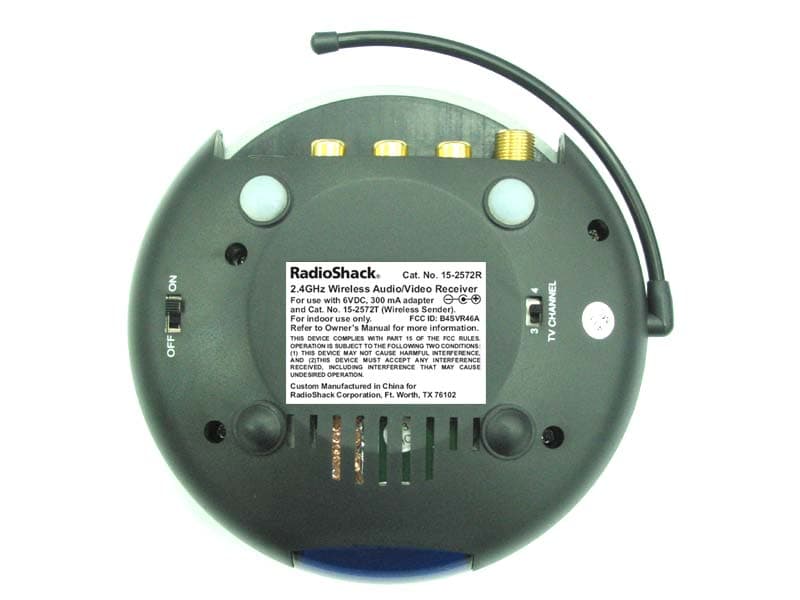
Click to zoom
Application Details
- Equipment Class
- DSC - Part 15 Security/Remote Control Transmitter
- Date of Grant
- Aug 22, 2006
- Application Purpose
- Original Equipment
- Date of Application
- Aug 22, 2006
- Equipment Note
- WIRELESS AUDIO/ VIDEO SENDER WITH IR EXTENDER
- Frequency Range
- 433.92000000 - 433.92000000
- Company
- Authinx Inc.
- Country
- United States
Documents & Files
Document Text
Text extracted from the exhibit documents filed with the FCC. Open a document above to read the original.
Users Manual
C AT . N O . 15-2572 W W W W W IRELESS IRELESS IRELESS IRELESS IRELESS A A A A A UDIO UDIO UDIO UDIO UDIO /V /V /V /V /V IDEO IDEO IDEO IDEO IDEO S S S S S ENDER ENDER ENDER ENDER ENDER with IR Extender Feature S ENDER 15-2572T OWNER’S MANUAL S ENDER 15-2572T 3 2 FCC C AUTION THIS DEVICE COMPLIES WITH PART 15 OF THE FCC RULES.OPERATION IS SUBJECT TO THE FOLLOWING TWOCONDITIONS:(1) THIS DEVICE MAY NOT CAUSE HARMFUL INTERFERENCE, AND (2) THIS DEVICE MUST ACCEPT ANY INTERFERENCE RECEIVED, INCLUDING INTERFERENCE THAT MAY CAUSEUNDESIRED OPERATION. NOTE: Modifications to this product will void the user’s authority to operate this equipment. I NTRODUCTION Your Wireless Audio/Video Sender system consists of a Sender unit whichyou connect to your satellite receiver, DVD player, etc., and a Receiverunit that you connect to a TV anywhere in your home. The Audio/VideoSender converts the A/V signal from your A/V product into a 2.4 GHzwireless Radio Frequency (RF) signal and transmits it (even through walls)to the Audio/Video Receiver unit. The Audio/Video Receiver converts thesignal back to an A/V signal and passes it through a cable to your TV’sCOAX input, or A/V input jacks.The Audio/Video Sender system also includes an IR Extender feature. Thislets you remotely control the A/V product that the Sender is connected to,from the location where the Receiver is located. For example, you cancontrol a DVD Player in your living room, while watching it on a TV inyour bedroom.There are just a few simple steps to follow to hook up your Audio/VideoSender system to a satellite receiver, VCR, DVD Player, or Cable Box. C ONTENTS I NTRODUCTION ........................................................................ 3 C ONTROLS AND C ONNECTIONS .................................................. 4 S ENDER ............................................................................ 4 R ECEIVER .......................................................................... 5 C ONNECTING U P ..................................................................... 6 H OOKING UP THE S ENDER .................................................... 6 H OOKING UP THE R ECEIVER ................................................. 8 F INE TUNING YOUR S YSTEM .................................................... 10 IR E XTENDER F EATURE ......................................................... 11 5 4 DC 6V CHANNEL ONOFF TV CHANNEL 34 ONOFF CHANNEL RF Antenna(for use with the IRExtender feature) Power Supply Jack 2.4 GHz Antenna 2.4 GHz Channel Switch A/V In Jacks 2.4 GHz ChannelSwitch (underneath2.4 GHz Antenna). C ONTROLS AND C ONNECTIONS Audio/Video Receiver Audio/Video Sender ON-OFF Switch (on side) A/V Out Jacks COAX out Channel 3/4 switch IR Extender Jack RF Antenna(for use with the IRExtender feature) Power Supply Jack ON-OFF Switch (on side) 7 6 Video Audio Out In Out Video Audio A /V Component Antenna To TVAntenna TV A /V Component Antenna To TVAntenna TV Out Video Audio UHF/VHFTo TVUHF/VHF C ONNECTING U P Hooking up the Audio/Video Sender1. Connect one set of Audio/Video cables to the VIDEO and AUDIO jacks of your Audio/Video Sender. Take care to match the colors of theplugs on the cable with the jacks on the Audio/Video Sender. 2. Connect the other end of the cable to the Audio/Video OUT jacks on your TV. Take care to match the colors of the plugs on the cable withthe jacks on the TV. If the jacks on the TV are colored differently,connect the yellow plug to the jack labelled VIDEO, the red plug to thejack labelled AUDIO RIGHT and the white plug to the jack labeledAUDIO LEFT. See diagram A below.Note: If your TV does not include Audio/Video OUT jacks, you will need to remake the connections as shown in diagram B) using theTV antenna (coaxial) connections to link up a Satellite Receiver(DBS), or Cable Box, or VCR, or DVD Player to your TV. 3. Plug the Audio/Video Sender’s Power Supply into a convenient 120 volt wall outlet and plug its jack into the Audio/Video Sender. 4. Position the Audio/Video Sender in a convenient location such as on top of your TV and orient the antenna so that the flat side points in thedirection of the room where you will be installing the Receiver. If you have several A/Vcomponents:If you have two or more A/Vcomponents (e.g. Satellite Receiver(DBS), VCR, Cable Box, DVD Player,etc.) that you want to watch in anotherroom, they will probably already behooked up to the local TV in series (seethe diagram to the right). To connect theAudio/Video Sender you just need toidentify the last component in the chainand connect its LINE OUT jacks to theAudio/Video Sender’s A/V IN jacks.If the last component in the chain doesnot have spare LINE OUT jacks,reconnect the local TV to the lastcomponent in the chain using a coaxialcable to connect to the VHF/UHF jack,then use the A/V connections for theAudio/Video Sender. A) Connections for a TV with A/V OUT jacks. B) Connections for a TV without A/V OUT jacks. A/V Cables CoaxialCable TV UHF/VHF Satellite Receiver Out Video Audio UHF/VHFTo TV In Cable Box Out Video Audio In DVD Player Out Video Audio In 9 8 Hooking up the Audio/Video Receiver1. Connect a set of Audio/Video cables to the A/V OUT jacks of your Audio/Video Receiver. Connect the other end to your TV. 2. Plug the Audio/Video Receiver’s Power Supply into a 120 volt wall outlet and plug its jack into the Audio/Video Receiver. 3. Position the Audio/Video Receiver in a convenient location such as on top of your TV and orient the antenna so that the flat side points in thedirection of the room where you set up the Audio/Video Sender. Video Audio In A /V Component TV Out Video Audio In Video Audio TV In UHF/VHF(COAX) In TV 1 2 TV UHF/VHFFrom antenna If your TV does not have A/V connectors:You can use the supplied coaxial cable to connect the TV OUT COAXsocket on the Audio/Video Receiver to the Antenna input on your TV. Ifyou already have an antenna connected to your TV, you will need to use aTV antenna splitter as shown belo…
Text truncated - open the document above for the full version.
Block Diagram
2.4GHz PatchAntenna SAW Video O/P Audio O/P (L) Audio O/P (R) 2.4GHz RF Receiver RF Demodulator IF LNA 6MFilter 6.5MFilter IR 433MHz transmitter Amplifier IR Sensor Block Diagram for Video Receiver VR46A
ID Label/Location Info
VR46A Rating Label 2.4GHz Wireless Audio/Video Receiver ® Cat. No. 15-2572R For use with 6 Cat. No. 15-2572T (Wireless Sender). For indoor use only. Refer to Owner’s Manual for more information. VDC, 300 mA adapter and Custom Manufactured in China for RadioShack Corporation, Ft. Worth, TX 76102 FCC ID: B4SVR46A THIS DEVICE COMPLIES WITH PART 15 OF THE FCC RULES. OPERATION IS SUBJECT TO THE FOLLOWING TWO CONDITIONS: (1) THIS DEVICE MAY NOT CAUSE HARMFUL INTERFERENCE, AND (2)THIS DEVICE MUST ACCEPT ANY INTERFERENCE RECEIVED, INCLUDING INTERFERENCE THAT MAY CAUSE UNDESIRED OPERATION. – + •
Operational Description
VR46A Operational Description-433 MHz transmitter: The VR46A contains a 433 MHz pulsed transmitter. The transmitter is used to extend Infrared Transmitter range. The Infrared Pulse Coded remote control TV/VCR/DVD commands are received by the VR46A and used as an input to the 433 MHz pulsed transmitter. This signal is then transmitted via the loop antenna to the VT46A, where the process is reversed.
Parts List/Tune Up Info
PART IDENTIFIERDESCRIPTIONQTY/ASSYREFERENCE AA15-2572RB=1U RS VIDEO RECEIVER NOPACK1 027016=10000COPPER FOIL TAPE, W=24MM0.015FOR IR RX BOARD 027=11000010TAPE-PVC 11MM UL510FR B K0.05 038010=10513-2 433 MC LABEL1 038010=11562DATE CODE (A&A)1 038020=12095A RATING LABEL 15-2572R1 183010=16300A RUBBER STAND2 183010=16390A ANTENNA COVER, VT30A1 183010=20541HINGE (TOP), SILVER1 183010=20551HINGE (BOTTOM), SILVER1 183010=20561A DISK (TOP), SILVE R1 183010=20571DISK (BOTTOM), SILVE R1 183010=20581DISK HOLDER, SILVER1 183010=20591A SWITCH COVER (R), SILVER1 183010=20610A ANTENNA HOLDER, PC+ABS1 183010=20620A PLASTIC TUBE1 183010=20630LENS1 185000=19831A TOP CABINET, SILVE R1 185000=20850A BOTTOM CABINET (WITH VHF)1 186002=10420REAR TRIM LABEL (R), VHF1 186003=10074 ANTENNA LABEL1 283=00000027SLIDE-SW,1P2T,SS12F891 363=22601000SINGLE SCREENED0.3550.275+0.08 365000=10023HOT MELT GLUE, HE-38 A1 391=60201020SCREW M2X6 MS/ZP2 391=60203030SCREW-PPTT M2.6X8 MS/ZP4 391=61503070SCREW-WHTT M2.6X6 DIM6.02 851001=11784 ANTENNA PCB ASSY1 042010=11131B PCB ANT. FR4 49X49X1.6MM1 363=00000031A COAXIAL RG178B/U 160MM1 851001=12576PCB ASSY 2.4G RX MODULE1 042010=11678A PCB, 2.4G R X1 076=10000022CAP-MCC 10P .25P COG 04027C8,19,29,40,41,45,48 076=10100024CAP-MCC 100PF 5% COG 04023C16,43,64 076=10200024CAP-MCC 1N 5% NPO 04026C3,18,34,56,72,74 076=10300028CAP-MCC 10N 10% X7R 04022C21.36 076=10400028CAP-MCC 100N 10% X7R 04024C20,33,37,63 076=10500028CAP-MCC 1U 10% X7R 040211REFER TO SCHEMATIC 076=10600016CAP-MCC 10U +8-2 Y5V 08055C6,22,28,51,52 076=12200024CAP-MCC 1N2 5% NPO 04021C23 076=15200024CAP-MCC 1N5 5% NPO 04021C24 076=18000024CAP-MCC 18P 5% COG 04022C13,14 076=20100024CAP-MCC 200P 5% NPO 04021C67 076=22100024CAP-MCC 220P 5% COG 04022C127,128 076=33000024CAP-MCC 33P 5% COG 04023C10,31,68 076=33900022CAP-MCC 3P3 .25P COG 04021C30 076=39000024CAP-MCC 39P 5% COG 04022C69,70 076=47000024CAP-MCC 47P 5% COG 04022C105,106 076=47100024CAP-MCC 470P 5% COG 04022C122,124 076=47200014CAP-MCC 4N7 10% X7R 06032C103,104 076=47300028CAP-MCC 47N 10% X7R 04023C1,2,5 076=47400028CAP-MCC 470N 10% X7R 04021C38 076=47500031CAP-MCC 4U7 +8-2 Y5V 06032C107,108 076=47900022CAP-MCC 4P7 .25P COG 04021C11 076=50800022CAP-MCC 0P5 .25P COG 04021C27 076=56900022CAP-MCC 5P6 .25P COG 04021C4 076=60900022CAP-MCC 6P .25P COG 04021C71 076=68100024CAP-MCC 680P 5% COG 04022C109,110 076=68900022CAP-MCC 6P8 .25P COG 04022C32,44 080=00000048CRYSTAL 8MHZ HC-49/S1X1 110=00000000CERAMIC FILTER 6M1F101 110=00000003SAW FILTER 480MHZ1F4 110=00000010CERAMIC FILTER 6M51F102 110=00000014MULTILAYER BF3216 2400ACT1F1 138001=1005310 WAY PIN HEADER 2.54MM1P1 160=12700018INDUCTOR 12NH 10% 0402SMD2L9,22 160=12900019INDUCTOR 1N2H 5% 0402 SMD1L3 160=18000003INDUCTOR 18UH 10%,0805SMD2L7,8 160=18700018INDUCTOR 18NH 10%0402 SMD1L6 160=39900019INDUCTOR 3N9H 5% 0402 SMD1L2 160=47600019INDUCTOR 4N7H 5% 0402 SMD3L1,4,5 209=00000001TRS-NPN 2N3904 SMD1Q2 209=00000020TRS-NPN BFS520 (SOT-23)1Q3 209=00000021TRS-NPN BFG425W, SOT-343R1Q1 211328=10383IC RTC6711 (QFN48A1)1U2 211328=10384IC RTC6721 (QFN24LD-B)1U101 211328=10385IC REGULATOR2.5V,SOT-23-51U4 241=00000003RES-TFC 0R 5% 1/10W 06031R16A 241=00000006RES-TFC 0R 5% 1/16W 04026C14,28,32,33,121,123 241=10300006RES-TFC 10K 5% 1/16W 04027R1,2,4,9,20,29,111 241=15300006RES-TFC 15K 5% 1/16W 04024R101-104 241=18200006RES-TFC 1K8 5% 1/16W 04021R25 241=18300006RES-TFC 18K 5% 1/16W 04021R3 241=20100006RES-TFC 200R 5% 1/16W04022R129,130 241=20200006RES-TFC 2K 5% 1/16W 04022R109,110 241=20300006RES-TFC 20K 5% 1/16W 04021R21 241=27400006RES-TFC 270K 5% 1/16W04021R7 241=30100006RES-TFC 300R 5% 1/16W04021R5 241=30300006RES-TFC 30K 5% 1/16W 04021R6 241=33300006RES-TFC 33K 5% 1/16W 04022R8,26 241=39200006RES-TFC 3K9 5% 1/16W 04023R11,12,16 241=39400006RES-TFC 390K 5% 1/16W04022R107,108 241=51000006RES-TFC 51R 5% 1/16W 04021R31 241=51200006RES-TFC 5K1 5% 1/16W 04021R30 241=56100006RES-TFC 560R 5% 1/16W04021R23 241=68000006RES-TFC 68R 5% 1/16W 04021R24 241=82200006RES-TFC 8K2 5% 1/16W 04022R105,106 403041=10116METAL BOX (B)1 851001=12633PCB ASSY,433RF (343)1 038010=10513-2 433 MC LABEL1 042010=10938A PCB1 076=10000014CAP-MCC 10P 5% NPO 06034C5,7,18,22 076=10100023CAP-MCC 100P 5% NPO 06031C6 076=10400019CAP-MCC 100N +8-2 Y5V06035C2,3,21,23,24 076=10500016CAP-MCC 1U +8-2 Y5V 08052C4,8 076=10900012CAP-MCC 1P .25P NPO 06031C25 076=12100023CAP-MCC 120P 5% NPO 06031C10 076=22000023CAP-MCC 22P 5% NPO 06031C12 076=22200014CAP-MCC 2N2 10% X7R 06031C1 076=25900012CAP-MCC 2P5 .25P NPO 06031C11 076=30900012CAP-MCC 3P .25P NPO 06032C28,29 076=47200014CAP-MCC 4N7 10% X7R 06031C30 076=50800012CAP-MCC 0P5 .25P NPO 06031C37 076=56000023CAP-MCC 56P 5% NPO 06032C13,20 076=70900012CAP-MCC 7P .25P NPO 06032C27,31 076=75800012CAP-MCC 0P75.25P NPO 06031C32 080=00000010SAW RESONATOR 433.92MHZ1Y1 162089=10050COIL 10T5R ID=1 WD=0.222L1,2 209=00000001TRS-NPN 2N3904 SMD5Q1-5 209=00000003TRS-NPN 2SC3356 SMD R251Q8 210117=10070TRS-NPN MPS H10 SMD1Q7 210=00000000TRS-PNP 2N3906 SMD1Q6 211328=10124IC 4069 SMD1U2 212107=10015DIODE-SI 1N4148, SMD1D1 212107=10016DIODE-DUAL BAV99 (SOT-23)1D2 224200=10000DIODE-P INFRARED PH302/2B1D5 241=10000003RES-TFC 10R 5% 1/10W 06031R23 241=10300003RES-TFC 10K 5% 1/10W 06033R6,14,17 241=10400003RES-TFC 100K 5% 1/10W06031R3 241=10500003RES-TFC 1M 5% 1/10W 06032R4,15 241=15100003RES-TFC 150R 5% 1/10W06031R18 241=15300003RES-TFC 15K 5% 1/10W 06031R13 241=18400003RES-TFC 180K 5% 1/10W06031R10 241=22500003RES-TFC 2M2 5% 1/10W 06031R8 241=33500003RES-TFC 3M3 5% 1/10W 06031R9 241=47000003RES-TFC 47R 5% 1/10W 06032R20,21 241=47300003RES-TFC 47K 5% 1/10W 06034R1,2,7,12 241=47400003RES-TFC 470K 5%1/10W 06031R11 241=47500003RES-TFC 4M7 5% 1/10W 06031R5 241=68200003RES-TFC 6K8 5% 1/10W 06032R16,19 241=82000003RES-TFC 82R 5% 1/10W 06031R22 358=60821001WIRE-JUMPER D=0.6MM1 403041=10051A IR COVER1 851001=12651PCB ASSY,6M/6M5,W/VHF1 042010=11734A PCB1 057=22000029CAP-E 22U 20% 16V2C5,6 057=22100014CAP-E 220U 20% 10V1C3 057=22100018CAP-E 220U 20% 25V1C1 057=4710…
Text truncated - open the document above for the full version.
Schematics
1 2 34 ABCD 4 3 2 1 D CBA Title Number Revision Size A4 Date: 27-Jun-2006 Sheet of File: C:\JOSEPH\SCH\MD40557R.SCH Drawn By: J4 DC JACK C1 220uF VI G VO REG1 H1117 SW2 1P2T C3 220u R7 1K5 LED1 3MM +3V3 16V 6V3 C2100nF C4100N VIDEO AUDIO R AUDIO L TO 2.4G Module +3V3 IN GND C6470U C7 22U C822U YellowRCA RedRCA White RCA R10 100K C11 22N C10 22N R9 100K R8 100K C9 100p +3V3 =11036-1.sch-1 - Tue Jul 18 12:28:16 2006 1 2 3 4 5 6 78 ABCD 8 7 6 5 4 3 2 1 D CBA Title Number Revision Size A3 Date: 14-Jun-2006 Sheet of File: A:\PWRMID-6.SCH Drawn By: ANTENNA 433.92MHz Powermid Tx R16 6K8 R1710K R18 150R R19 6K8 R20 47R R21 47R C25 1P C11 2P5 C23 100N C12 22P C13 56P C19 100NC28 3P C27 7P C18 10P C31 7P Y1 433.92MHz Q7 H10 Q8 2SC3356 L1 10T5R L2 10T5R +3V3 C37 0P5 +3V3 PCB1 PCB2 C29 3P +3V3 C20 56P C10120P C26 * U2C 4069 U2B4069 U2A4069 Q6 3906 R15 1M C24 100N U2E4069 U2F4069 R13 15K C5 10P C7 10P C6 100P R14 10K C22 10P C320P75 R22 82R D1 1N4148 D2 BAV99 D5 PH302/2B C36 * R3 100KQ1 3904 Q2 3904 Q3 3904 R5 4M7 R4 1M R1 47K R7 47K R2 47K C3 100N R8 2M2 R6 22K +3V3 R10 180K R9 3M3 Q4 3904 Q5 3904 C30 4N7 R11 470K R12 47K C1 2N2 C2 100N C4 1U C21 100N IR DATA IR DATA 13 12 C8 1U 11 10 123456 PCB : 042010=10938A R23 10R NOTE : ALL UNSPECIFIED RESISTOR & CAPACITOR ARE USE 0603 SMD TYPE 01 PCB ASSY : 851001H12633 14 7 +3V3 10KHz SWITCH INPUT 11 22 33 44 D D C C B B A A 1 SYS TEM X -10 LTD. 2 AV Rx H1 16 78 -1 *D: \7 kam\10 WORK\ 2G 4\RW6 7 s eries-X T\6 7Rx\ =116 78 P-1 .SCHDO C Ti tl eSize: No: Dat e:File: Revision:Sheet of A4 Cann ot open fil e E: \D ocument s an d Sett in gs\ cheng chi a\ My 22-Jun-06 1 2 3 4 SAW_FILTERF4 6. 8pF C44 1u F C46 8MHZ X1 18 pFC13 18 pFC14 33 KR8 10 pFC40 4. 7nHL5 30 KR6 33 pF C31 1. 5nFC24 3. 3pFC30 27 0K R7 10 pF C29 30 0R5 1. 2nF C23 10 0n FC37 47 0n F C38 1u FC53 10 0n F C63 10 pFC8 1. 2nh L3 NPC9 10 K R9 10 pF C45 4. 7nH L4 6. 8pF C32 10 pF C19 10 0n F C20 10 0n F C33 +2.5V +3.3V +2.5V +2.5V+2.5V +2.5V +2.5V +3.3V 1 2 3 4 5 6 7 8 9 10 10 PIN P1 Vi deo Au di o_6 .5MAu di o_6 M X2X1 +2.5V CS2 CS1 CS0 +2.5V +3.3V +3.3V +5V 18 nH L6 +2.5V 0RR14 NP R10 X1 X2 Vi deo 0. 5pFC27 3. 9KR12 1n F C18 1u F C17 10 0p FC16 1u FC7 1u F C26 10 0p F C64 1u F C52 10 pF C48 10 pF C41 1n FC34 1u FC35 3. 9kR11 20 0p FC67 1u FC42 47 nF C5 47 nF C2 47 nF C1 +2.5V 1u FC47 10 KR210 KR1 10 K R4 +3.3V 0RR28 SPI NP R27 10 K R29 BX SPI 51R31 1u FC76 BX IF-IN IF-OUT RF VA MPIN 1 SMA-9BJ1 4. 7pFC11 33 pF C10 1n F C3 3. 9nHL2 18 k R3 BF2520-B2R4DABA F1 5. 6pF C4 4. 7nHL1 +2.5V BFG425WQ1 AN T RF 3. 9KR16 33 pF C68 18 uH L7 39 04 Q2 10 KR2020 K R21 56 0R23 1. 8KR25 18 uH L8 39 pF C70 1u FC60 39 pF C69 BBOUT2 +3.3V 68 R R24 10 uFC62 10 uF C51 NP C75 VA MPIN 10 uF C28 10 uFC2210 uF C6 +5V +3.3V VIN /1 1 GN D/2 2 EN /3 3 BP/4 4 VO UT/ 5 5 RT9 167 A-25 21 13 28=1 03 85 U4 +2.5V 10 nFC36 0RR32 NPR13 12 nHL9 1n F C72 6p F C71 12nH L2 2 33K R26 +3.3V BFS520 Q3 1n FC56 1n FC74 10 0p FC43 IF-IN IF-OUT Au di o-RTC67 21#N AME? 5. 1KR30 +2.5V +5V BX CS2 CS1 CS0 PD_REG18 1 LN AV DD 2 RFIN2 3 SPI_D AT A/ CH2 4 SPILE/CH1 5 SPICLK/CH0 6 SPI_SE 7 BX 8 VD D3 D 9 VSS_SYN3 10 BCR 22 VA MPRE F 28 XT AL2 13 LO CK _D T 14 CP 15 VD D_SY N 16 S2 17 VT 2G 18 VCO2 GV DD 19 BBOUT2 29 IFINP 23 FSKCOMIN 27 HY S_ C 39 BBVDD 1 41 VA MPIN 30 VA MPV DD 31 VA MPO UT 32 TH D_ C 33 FSKCOMOUT 40 SLICER_RC 37 IFAOU TP 43 VD D33 _IFA 44 X1 35 X2 36 IFAVD D 45 RFGND 46 AG C_C 25 BBVDD0 26 VCO5DVDD1 34 IFAOU TN 42 VSS_SYN4 11 XT AL 1 12 VD D2D 5 20 REG1 D8 21 FSKVD D 38 IFINN 24 RFIN 47 LN A_L G 48 GN D 49 RTC6711A U2 0RR16A NP VR1 1 2 3 3PIN-AJ1 A 0603 20 9-0 000 002 0 211328=10383 20 9-0 000 002 1 11 0-0 000 001 6 Ass'y: 8 5100 1=12 576 2G4 RX - RT A 011B 1 01C 1 10D 111 US/EUR2414 M2432 M2450 M2468 M Ch CS0-2 AUS 2414 M2432 M2450 M 0RR33 11 22 33 44 D D C C B B A A 2 SYS TEM X -10 LTD. 2 AV Rx H1 16 78Q -1 *D: \7 kam\10 WORK\ 2G 4\RW6 7 s eries-X T\6 7Rx\ =116 78 Q-1. SCHD OC Ti tl eSize: No: Dat e:File: Revision:Sheet of A4 Cann ot open fil e E: \D ocument s an d Sett in gs\ cheng chi a\ My 22-Jun-06 6. 5M11 0-0 000 001 0F1016. 0M 11 0-0 000 000 0 F102 Au di o_6 M Au di o_6 .5M BBOUT2 NPC111 +3.3V +3.3V NPC112 10 KR111 39 0KR108 47 pFC106 15 kR10415 kR103 +3.3V NPC102 15 kR10215 kR101 +3.3V NPC101 2kR110 4. 7nF C104 68 0p F C110 2k R109 4. 7nF C103 68 0p F C109 12 kR106 4. 7uFC108 39 0KR107 47 pFC105 12 kR105 4. 7uFC107 NP Q1 01 NPR121 NP R122 NP R123 47 0p FC122 +5V 0R C121 NPQ1 02 NPR124 NP R125 NP R126 47 0p FC124 +5V 0RC123 NPC125 NPC126 NP R127 NPR128 20 0R129 20 0R130 VD_VCO2 1 VSS 2 VSS 3 VSS 4 AO2 5 IN2 6 IP2 7 FIR2 8 VSS 9 FIR1 10 IP1 11 IN 1 12 AO1 13 PD_BUF 14 LOCK 15 LOCK_L_B 16 PD_AMP 17 VD_VCO1 18 VD1 19 FM1 20 VBG_ 10K 21 PD_AU 22 FM2 23 VD2 24 25 25 RTC6721211328=10384U1 01 22 0p FC12722 0p FC128 Ass'y: 8 5100 1=12 576 2G4 RX - RT Det ail By Dat e 11 67 8A-A 3 Kam 20 06 062 2
Test Report
Retlif Testing Laboratories, Test Report No. R-11570-1, X-10 (USA), FCC ID: B4SVR46A Page 1 of 21 Technical Information APPLICANT MANUFACTURER Name: X10 (USA), Inc. Name: X-10 Electronics (Shenzhen) Co. Ltd. Address: 19823 58 th Place South Address: Together Rich Industrial Park B Sanwei Industrial District, Xixiang Town City, State, Zip: Kent, WA 98032 City, State, Zip: Baoan County, Shenzhen, China Test Specification: FCC Rules and Regulations Part 15, Subpart C, Para. 15.231 Test Procedure: ANSI C63.4:2003 Test Sample Description Test Sample: 433 MHz Pulsed Transmitter Brandname(s): X10 (USA) Model Number: VR46A and RadioShack Cat. No. 151-2572T FCC ID: B4SVR46A Type: Pulsed Transmitter Power Requirements: 6 VDC derived from external AC Adapter Frequency of Operation: 433 MHz Applicable Rule Section: Part 15, Subpart C, Section 15.231 Tests Performed Para. 15.207(a), Conducted Emissions Para. 15.231(a), Radiated Emissions, Fundamental and Harmonics Para. 15.231(b), Radiated Emissions, Spurious Case Para. 15.231(b), Duty Cycle Determination Para. 15.231(c), Occupied Bandwidth Retlif Testing Laboratories, Test Report No. R-11570-1, X-10 (USA), FCC ID: B4SVR46A Page 2 of 21 Test Results 15.207(a): The radio frequency voltage that was conducted back on to the AC power line on any frequency/frequencies within the bandwidth of 150 kHz to 30 MHz did not exceed Class B limits as specified in CISPR 22. 15.231 (a): This device transmits a control signal and is used as a remote control transmitter. 15.231 (a)(2) The transmitter is automatically operated. Transmission ends 5 seconds after activation. 15.231 (a)(3): The transmitter does not perform periodic transmissions or the transmitter performs periodic transmissions at predetermined intervals greater than 1 hour apart and are shorter than 1 second in duration. 15.231 (b): The fundamental field strength did not exceed11000 μV/M (Average) at a test distance of 3 meters. In addition, the requirements of section 15.35 for averaging pulsed emissions and for limiting peak emissions were met. The field strength of harmonic and spurious emissions did not exceed 1100 μV/M (AVERAGE). 15.231 (c) The Bandwidth of the emission was no wider than 0.25% of the center frequency (1083 kHz) as measured 20 db down from the modulated carrier. Retlif Testing Laboratories, Test Report No. R-11570-1, X-10 (USA), FCC ID: B4SVR46A Page 3 of 21 Determination of Field Strength Limits The field strength limits shown below are found in Section 15.231: Frequency Limit F1 = 260 3750 = L1 Fo = 433 MHz Lo F2 = 470 12500 = L2 The formula below was utilized to determine the limits: Limit = L1 + [(Fo-F1)(L2-L1)/(F2-F1)] Solving Yields Fundamental Limit = 11000 μV/M (AVERAGE) @ 3 Meters Harmonic Limit = 1100 μV/M (AVERAGE) @ 3 Meters Duty Cycle Determination The unit’s RF output was directly coupled to the input of the spectrum analyzer. The analyzer was set for a frequency span of 0 Hz. The sweep time was then adjusted in order to display one full pulse train. The transmitter on time was then summed and compared to the time for one full cycle in order to obtain the duty cycle. (See plots for additional information.) Transmitter On Time = 26.62 milliseconds (maximum per cycle) Transmitter Cycle Time = 102.4 milliseconds (100 ms maximum) Transmitter Duty Cycle =26.6 % Calculation 1 Large Pulse =8.8 milliseconds 33 x 540 μs (small pulse) = 17.82 milliseconds 8.8 + 17.82= 26.62 milliseconds Duty Cycle (XX/100) =26.6 % Correction Factor =20 log (0.XX)= -11.5 dB Retlif Testing Laboratories, Test Report No. R-11570-1, X-10 (USA), FCC ID: B4SVR46A Page 4 of 21 Spectrum Analyzer Desensitization Considerations Due to the nature of the emissions being measured, care was taken to ensure that the resolution bandwidth of the spectrum analyzer was adequate to provide accurate measurements. The following formula was utilized: minimum bandwidth = 1/{minimum pulse width (in seconds) x 1.5} = Hz Setting pulse desensitization equal to zero and utilizing the minimum observed pulse width of 540 μs yields a minimum required bandwidth of 1,234.0 Hz. FCC specified bandwidths of 100 kHz and 1 MHz were utilized below and above 1 GHz, respectively. General Notes 1. All readings were taken utilizing a peak detector function at a test distance of 3 meters. 2. The duty cycle was applied to the peak readings in order to determine the average value of the emissions. 3. The frequency range was scanned from 30 MHz to 4.4 GHz. All emissions not reported were more than 20 dB below the specified limit. Retlif Testing Laboratories, Test Report No. R-11570-1, X-10 (USA), FCC ID: B4SVR46A Page 5 of 21 Certification and Signatures We certify that this report is a true representation of the results obtained from the tests of the equipment stated. We further certify that the measurements shown in this report were made in accordance with the procedures indicated and vouch for the qualifications of all Retlif Testing Laboratories personnel taking them. Donald C. Lerner EMC Test Engineer Richard J. Reitz Laboratory Manager Non-Warranty Provision The testing services have been performed, findings obtained and reports prepared in accordance with generally accepted laboratory principles and practices. This warranty is in lieu of all others, either expressed or implied. Non-Endorsement This test report contains only findings and results arrived at after employing the specific test procedures and standards listed herein. It is not intended to constitute a recommendation, endorsement or certification of the product or material tested. This test report must not be used by the client to claim product endorsement by NVLAP or any agency of the U.S. Government. Retlif Testing Laboratories, Test Report No. R-11570-1, X-10 (USA), FCC ID: B4SVR46A Page 6 of 21 FCC Part 15, Subpart C, Conducted Emissions, Power Leads, Test Data Retlif Testing Laboratories, Test Report No. R-11570-1, X-10 (USA), FCC ID: B4SVR46A Page 7 of 21 Retlif Testing …
Text truncated - open the document above for the full version.
Test Setup Photos
Retlif Testing Laboratories, Test Report No. R-11570-1, X-10 (USA), FCC ID: B4SVR46A Page 1 of 3 Conducted Emissions, Rear Test Setup Conducted Emissions, Front Test Setup Retlif Testing Laboratories, Test Report No. R-11570-1, X-10 (USA), FCC ID: B4SVR46A Page 2 of 3 Occupied Bandwidth and Duty Cycle, Test Setup Radiated Emissions, Rear Test Setup Retlif Testing Laboratories, Test Report No. R-11570-1, X-10 (USA), FCC ID: B4SVR46A Page 3 of 3 Radiated Emissions, Front Test Setup
Contact Information
Applicant
Shane Houshmand(Chief Operating Officer)
Test Firm
Retlif Testing LaboratoriesMichael Bozza
Technical Specifications
| # | Rule Parts | Frequency Range | Power Output |
|---|---|---|---|
| 1 | 15.231 | 433.92 MHz - 433.92 MHz | - |
Other Applications from Authinx Inc.

B4SXC35A
Jun 16, 2011Wireless Color Camera
Equipment Class
DXX - Part 15 Low Power Communication Device Transmitter
B4SVT50
Jun 16, 2011Wireless Audio/Video System
Equipment Class
DXX - Part 15 Low Power Communication Device Transmitter
B4SVR50
Jun 13, 2011Wireless Audio/Video Receiver
Equipment Class
DSC - Part 15 Security/Remote Control Transmitter
B4S-XC30A
Jun 07, 2011Wireless Color Camera
Equipment Class
DXX - Part 15 Low Power Communication Device Transmitter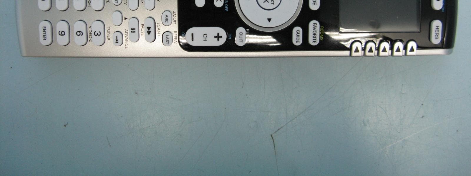
B4SIR34A
Aug 01, 2010Remote Control Transmitter
Equipment Class
DSC - Part 15 Security/Remote Control Transmitter