BAB271000297Millimeter Wave Radar
DENSO TEN Limited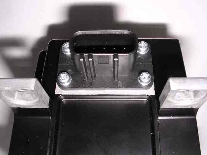
Click to zoom
Application Details
- Equipment Class
- FDS - Part 15 Field Disturbance Sensor
- Date of Grant
- Aug 17, 2004
- Application Purpose
- Original Equipment
- Date of Application
- Aug 17, 2004
- Equipment Note
- Millimeter Wave Radar
- Frequency Range
- 76000.00000000 - 77000.00000000
- Company
- DENSO TEN Limited
- Country
- Japan
Documents & Files
Document Text
Text extracted from the exhibit documents filed with the FCC. Open a document above to read the original.
Cover Letter(s)
Re: Certification for FUJITSU TEN 271000-2970 Radar Model: 271000-2970 FCC ID: BAB271000297 IC: 2024B-271297 POWER OF ATTORNEY A letter granting Valdis V. Liepa the Power of Attorney is on file and can be provided when so requested. Re: Certification for FUJITSU TEN 271000-2970 Radar Model: 271000-2970 FCC ID: BAB271000297 IC: 2024B-271297 REQUEST FOR CONFIDENTIALITY Pursuant to 47 CRF 0.459, FUJITSU TEN LIMITED requests that a part of the subject application be held confidential. This comprises Exhibits (4) Block Diagram and Equipment Specification (5) Schematics (9) Internal Photos (10) Parts List & Parts Placement (12) Description of Operation FUJITSU TEN LIMITED has spent substantial effort in developing this product and it is one of the first of its kind in industry. Having the subject information easily available to "competition" would negate the advantage they have achieved by developing this product. Not protecting the details of the design will result in financial hardship. If there are any questions regarding this request, please contact me at the above address or call 734-483-4211, fax 734-647-2106 or e-mail [email protected]. Sincerely, Valdis V. Liepa Research Scientist University of Michigan August 3, 2004 Re: Certification for FUJITSU TEN 271000-2970 Radar Model: 271000-2970 FCC ID: BAB271000297 IC: 2024B-271297 STATEMENT OF MODIFICATIONS There were no modifications made to the DUT by this test laboratory. (Also see Section 3.1 of the attached Test Report). _____________________ Valdis V. Liepa Research Scientist Re: Certification for FUJITSU TEN 271000-2970 Radar Model: 271000-2970 FCC ID: BAB271000297 IC: 2024B-271297 GENERAL PRODUCT INFORMATION The device, for which certification is pursued, has been designed by: FUJITSU TEN LIMITED 2-28, Gosyo-dori, 1-chome, Hyogo-ku, Kobe, 652-8510, Japan Naoto NISHIMURA, Engineering Support Department Research & Development. Group Tel: +81-78-682-2159 Fax: +81-78-671-7160 Canadian Contact: Fujitsu Ten Canada, Inc. 1149 Bellamy Road N. Unit 1, Scarborough, Ontario M1H 1H7 Tetsuya Yamamoto 416-431-9332 416-431-1745 [email protected]
Cover Letter(s)
American Telecommunications Certification Body Inc. 6731 Whittier Ave, McLean, VA 22101 August 13, 2004 RE: Fujitsu Ten Limited FCC ID: BAB27000297 After a review of the submitted information, I have a few comments on the above referenced Application. 1) Internal photographs can not simply be held confidential. Further justification must be provided before confidentiality can be granted on these exhibits. Additionally, if only certain pages of this exhibit are to be held confidential, then the exhibit must be separated into 2 parts, one not held confidential, and one that is. 2) The parts list provided does not appear to be covered by confidentiality. Please confirm or correct the confidentiality exhibit. 3) Peak power appears to be possible to +5 dBm per the 2 nd page of the block diagram. This is much different than expected. Please explain and/or fix. 4) Is a photograph of the PCB layout Photo-2 (RF-unit solder-side) available without the metal “bar” across the board? 5) It appears that only part of the RF schematics may have been provided. Please explain and/or provide as necessary. 6) Please provide an appropriate labeling exhibit for this device. IC Issues 7) The application form specifies D1N emissions, while the block diagram page 2, and the FCC application shows P0N and QXN. Please provide justification for the emissions designator. 8) Please provide the missing forms mentioned in your message regarding this application. Timothy R. Johnson Examining Engineer mailto: [email protected] The items indicated above must be submitted before processing can continue on the above referenced application. Failure to provide the requested information may result in application termination. Correspondence should be considered part of the permanent submission and may be viewed from the Internet after a Grant of Equipment Authorization is issued. Please do not respond to this correspondence using the email reply button. In order for your response to be processed expeditiously, you must submit your documents through the AmericanTCB.com website. Also, please note that partial responses increase processing time and should not be submitted. Any questions about the content of this correspondence should be directed to the sender.
Cover Letter(s)
American Telecommunications Certification Body Inc. 6731 Whittier Ave, McLean, VA 22101 August 13, 2004 RE: Fujitsu Ten Limited FCC ID: BAB27000297 After a review of the submitted information, I have a few comments on the above referenced Application. 1) Is a photograph of the PCB layout Photo-2 (RF-unit solder-side ) available without the metal “bar” across the board? 2) It appears that only part of the RF schematics may have been provided. Please explain and/or provide as necessary. 3) 4) Please provide an appropriate labeling exhibit for this device. 5) According to the mm wave procedures, the EWB should be based on the 26 dB bandwidth, not 20 dB. Please provide the proper EWB. Note that the application mentions several modulations, including FM and CW. What is the worse case EWB for each modulation, especially CW. First impressions is that the EBW is close to 110 MHz. Is this actually the EWB? 6) It appears that the emissions were not adjusted by 10 log (EWB/RBW). Please correct or explain why this was not necessary. 7) Mobile RF exposure information was calculated for safe distance. Note that the FCC is not interested in should be calculated for 20 cm distance, not safe distance. 8) None of the plots appear to be labeled. Plot 5.6 is referenced as if showing both FM and CW. No such plot appears to be provided. Please explain. 9) Plot 5.6 is referenced as if showing both FM and CW. No such plot appears to be provided. Please explain. 10) It appears that the Peak to Average Ratio given in 6.1 is based upon the 2/3 TX On/Off time. How does the CW modulation affect this calculation in 6.1. 11) Regarding the duty cycle, is there circuitry to determine if there is a mechanical problem with the positioner of the device. For instance, if the positioner stops working, what will be the duty cycle? 12) Page 14 mentions Class A limits. Class A does not appears to be relevant. Additionally, please explain the test distance associated with “Digital Device Emissions”. 13) Please explain the derivation of dBm/cm^2 to uW/cm^2. and dBuV/m to dBm/cm^2. IC Issues 14) The application form specifies P0N on the 731 and PQN on the IC form. Please justify or correct as necessary. Timothy R. Johnson Examining Engineer mailto: [email protected] The items indicated above must be submitted before processing can continue on the above referenced application. Failure to provide the requested information may result in application termination. Correspondence should be considered part of the permanent submission and may be viewed from the Internet after a Grant of Equipment Authorization is issued. z Page 2 August 13, 2004 Please do not respond to this correspondence using the email reply button. In order for your response to be processed expeditiously, you must submit your documents through the AmericanTCB.com website. Also, please note that partial responses increase processing time and should not be submitted. Any questions about the content of this correspondence should be directed to the sender.
Cover Letter(s)
1) Internal photographs can not simply be held confidential. Further justification must be provided before confidentiality can be granted on these exhibits. Additionally, if only certain pages of this exhibit are to be held confidential, then the exhibit must be separated into 2 parts, one not held confidential, and one that is. The internal photographs are requested as confidential as the DUT radome is epoxy sealed to the device, and cannot be removed without damage to the device. Previous filings of similar radar systems have held this as sufficient justification to keep all internal photographs confidential. 2) The parts list provided does not appear to be covered by confidentiality. Please confirm or correct the confidentiality exhibit. The confidentiality exhibit has been corrected and re-uploaded. 3) Peak power appears to be possible to +5 dBm per the 2nd page of the block diagram. This is much different than expected. Please explain and/or fix. The 5 dBm value in the equipment specification is a design source specification that does not account for loss in the system (antenna losses and interconnect transmission line losses). The EIRP, as computed in the test report from measured radiated emissions, is a more accurate method of determining the power rating of the DUT, since antenna efficiency and transmission line losses are not directly provided. 4) Is a photograph of the PCB layout Photo-2 (RF-unit solder-side ) available without the metal “bar” across the board? A photograph has been requested, and if available that photo will be provided. However, please note that this particular metal assembly is the mounting structure / heatsink of the MMIC, and separation of the ground metal from the device will likely destroy the MMIC. (This may be liked to removing the packaging from an IC.) No recognizable components will lye between the metal structure and the MMIC wafer, as this structure simply acts as a heatsink for the components within the MMIC structure. 5) It appears that only part of the RF schematics may have been provided. Please explain and/or provide as necessary. A request has been made with the manufacturer for more complete schematics of the RF subsection, and if available they will be provided. However, much of the high frequency RF sub-system is enclosed in the MMIC device; custom manufactured for this application and pre-packaged as the PCB RF UNIT. Since, in general, RF schematics of commercial RFIC’s are not required during certification (only block diagram information), it may be expected that the schematics for a similar MMIC structure (which may be the property of a third party vendor) also would not be required. Please comment on the requirement for RF schematics of RFIC’s and MMIC’s during the certification process so that we may proceed in acquireing the schematics requested. 7) The application form specifies D1N emissions, while the block diagram page 2, and the FCC application shows P0N and QXN. Please provide justification for the emissions designator. A corrected IC application form has been uploaded. Thank you
Cover Letter(s)
August 17, 2004 RE: Fujitsu Ten Limited FCC ID: BAB271000297 The following is in response to the comments made on this application: 1) Is a photograph of the PCB layout Photo-2 (RF-unit solder-side) available without the metal “bar” across the board? A photograph has been requested, and if available that photo will be provided. However, please note that this particular metal assembly is the mounting structure / heatsink of the MMIC, and separation of the ground metal from the device will likely destroy the MMIC. (This may be liked to removing the packaging from an IC.) No recognizable components will lye between the metal structure and the MMIC wafer, as this structure simply acts as a heatsink for the components within the MMIC structure. 2) It appears that only part of the RF schematics may have been provided. Please explain and/or provide as necessary. A request has been made with the manufacturer for more complete schematics of the RF subsection, and if available they will be provided. However, much of the high frequency RF sub-system is enclosed in the MMIC device; custom manufactured for this application and pre-packaged as the PCB RF UNIT. Since, in general, RF schematics of RFIC’s are not required during certification (only block diagram information), it may be expected that the schematics for a similar MMIC structure (which may be the property of a third party vendor) also would not be required. Please comment on the requirement for RF schematics of RFIC’s and MMIC’s during the certification process so that we may proceed in acquiring the schematics requested. 4) Please provide an appropriate labeling exhibit for this device. Our apologies, the exhibit has been uploaded. 5) According to the mm wave procedures, the EWB should be based on the 26 dB bandwidth, not 20 dB. Please provide the proper EWB. Note that the application mentions several modulations, including FM and CW. What is the worse case EWB for each modulation, especially CW. First impressions is that the EBW is close to 110 MHz. Is this actually the EWB? 110 MHz is the max-held measurement of total chirp/CW bandwidth while in the standard FM(chirp)/CW modulation mode. It does not represent the instantaneous bandwidth (EBW) of the chirp/CW radar. An updated test report has been uploaded which demonstrates the CW EBW of the radar. 6) It appears that the emissions were not adjusted by 10 log (EWB/RBW). Please correct or explain why this was not necessary. Please see the updated test report. Therein, the EWB of the radar is demonstrated to be lower than the input bandwidth of the Spectrum Analyzer used during the peak power measurement. 7) Mobile RF exposure information was calculated for safe distance. Note that the FCC is not interested in should be calculated for 20 cm distance, not safe distance. The RF Exposure exhibit has been modified and re-uploaded as requested. 8) None of the plots appear to be labeled. Plot 5.6 is referenced as if showing both FM and CW. No such plot appears to be provided. Please explain. A revised test report has been uploaded. In addition, figure 5.6 demonstrates the CW and FM emissions time of operation and is correct. This plot demonstrates the CW and FM signals at a frequency other than the CW center frequency. Thus, the FM emission is shown as a high-pulse in time, while the CW emission is shown as a low period. 9) Plot 5.6 is referenced as if showing both FM and CW. No such plot appears to be provided. Please explain. See above. 10) It appears that the Peak to Average Ratio given in 6.1 is based upon the 2/3 TX On/Off time. How does the CW modulation affect this calculation in 6.1. Peak emissions from the DUT were measured using CW (no switching or FM) with the antenna physically scanning. Since the peak emission was directly measured (possible because the scanning rate is slow – 5 Hz), the total duty factor applied to determine the average power is the complete -6.5 dB as calculated in Section 6.1 of the Test Report. 11) Regarding the duty cycle, is there circuitry to determine if there is a mechanical problem with the positioner of the device. For instance, if the positioner stops working, what will be the duty cycle? The DUT will not function correctly if the mechanical scanning mechanism is dysfunctional, and thus the device should be replaced. However, if the positioner where to fail, the duty cycle of the device would then be increased by the 2(2.7/16) ratio (see Section 6.1), resulting in an overall peak to average power duty factor of -3.6 dB. Also note that the device is only functional while the automobile is moving. 12) Page 14 mentions Class A limits. Class A does not appear to be relevant. Additionally, please explain the test distance associated with “Digital Device Emissions”. Digital device emissions are measured at a 3 meter distance. Digital emissions were measured so as to characterize the device, but since the system is for vehicular use only, they are not subject to regulation. 13) Please explain the derivation of dBm/cm^2 to uW/cm^2. and dBuV/m to dBm/cm^2. dBm/cm 2 to uW/cm 2 : 10 Log 10 (uW/cm 2 ) – 30 dB = dBm/cm 2 dBuV/m to dBm/cm 2 : S (mW/cm 2 ) = EIRP (mW) / (4 π R 2 ) EIRP (dBm) = S (dBm/cm 2 ) + 10 Log 10 (4 π R(cm)^2) EIRP (dBm ) = Pr (dBuV/m) – 95.2 dB Thus, at a 3m distance: Pr (dBuV/m) = S (dBm/cm 2 ) + 10 Log 10 (4 π (300)^2) + 95.2 dB = S (dBm/cm 2 ) + 155.74 dB IC Issues 14) The application form specifies P0N on the 731 and PQN on the IC form. Please justify or correct as necessary. The typographical error has been corrected. Please see the updated application forms exhibit.
External Photos
External Photo-1 Right side Front side Left side Underside Backside Upper surface External Photos External Photo-2 (Expansion of a connector part)
ID Label/Location Info
ID label ID label Location
RF Exposure Info
RF Exposure The minimum separation distance calculated following FCC OET Bulletin 65 is calculated as follows, where S is power density, Smeas (3m) = -27.9 dBm/cm 2 (pk; from Table 5.2, ave + duty factor) = 0.00162 mW/cm 2 = 12.1 dBm/m 2 EIRP = Smeas (3m) x 4pR 2 = 12.1 + 20.5 = 32.6 dBm = 1820 mW = 1.82 W ERP = EIRP – 2.15 = 32.6 – 2.15 = 30.5 dBm = 1110 mW = 1.11 W The power density at 20 cm is thus S(mW/cm 2 ) = EIRP(mW)/(4p R(cm) 2 ) = 0.36 mW/cm 2 NOTE: (1) Under no circumstances is the ERP of this device greater than 3W, as required by 2.1091 and the FCC mm-wave accepted test procedures, (2) The DUT is only operating when the vehicle is in motion
Test Report
FCC ID: BAB271000297 IC: 2024B-271297 Figure 5.1 Fundamental Spectrum; 3 meters, peak hold Figure 5.2 Time response at set frequency due to chirp, single scan. Figure 5.3 Time response at set frequency due to the antenna scan. Figure 5.3 Time response at set frequency due to antenna scan, 3 meters. Figure 5.4 Peak Power Measurement for CW scanning emission, 3 meters. Figure 5.5 Tx/Rx switching; 3 meters , LO=12.8417 GHz . Figure 5.6 FM/CW ratio; 3 meters. Figure 5.7 CW EBW measurement. LO = 12.833 GHz D UT on OATS (< 1GHz) D UT - Microwave Measurements Close-up D UT - mm-Wave Measurements
Contact Information
Applicant
Kaoru Abe(Department General Manager)
Technical Contact
University of Michigan/EECSValdis V Liepa
[email protected]734-483-4211
1301 Beal Ave. · Ann Arbor, Michigan · United States
Non-Technical Contact
University of Michigan/EECSValdis V Liepa
[email protected]734-483-4211
Test Firm
University of MichiganValdis Liepa
Technical Specifications
| # | Rule Parts | Frequency Range | Power Output |
|---|---|---|---|
| 1 | 15.253 | 76.00 GHz - 77.00 GHz | - |
Other Applications from DENSO TEN Limited
BABTN0052E
May 26, 2026Car Audio
Equipment Class
CXX - Communications Rcvr for use w/ licensed Tx and CBsBABTN0051A
Apr 10, 2026Car Navigation
Equipment Class
CXX - Communications Rcvr for use w/ licensed Tx and CBs
BABTN0046A
Feb 12, 2024Car Audio
Equipment Class
CXX - Communications Rcvr for use w/ licensed Tx and CBs
BABTN0040B
Jul 23, 2023Car Audio
Equipment Class
DTS - Digital Transmission System
BABTN0040A
Jul 23, 2023Car Audio
Equipment Class
CXX - Communications Rcvr for use w/ licensed Tx and CBs