CJJ79XITS-7037ITFS/MMDS Broadband Translator
Axcera
Click to zoom
Application Details
- Equipment Class
- AMP - Amplifier
- Date of Grant
- Apr 02, 2000
- Application Purpose
- Original Equipment
- Date of Application
- Nov 30, 1999
- Equipment Note
- ITFS/MMDS Broadband Translator
- Frequency Range
- 2500.00000000 - 2690.00000000
- Company
- Axcera
- Country
- United States
Documents & Files
Document Text
Text extracted from the exhibit documents filed with the FCC. Open a document above to read the original.
Users Manual
Telecommunications TECHNICAL MANUAL EXHIBIT II (PRELIMINARY) 6457A BROADBAND TRANSLATOR REV: 0 102 Rahway Road McMurray, PA 15317 USA Phone 412-941-1500 FAX 412-941-9421 ADC 6457A BROADBAND TRANSLATOR TABLE OF CONTENTS I.INTRODUCTION: II.SYSTEM 6457A: A. SYSTEM DESCRIPTION B. SPECIFICATIONS C. INSTALLATION PROCEDURE IIIOPERATION 6459A: A. SYSTEM CHECK OUT AND OPERATION B. INITIAL TURN ON C. NORMAL OPERATION D. FRONT PANEL CONTROLS (TRANSLATOR TRAY) E. INTERNAL INDICATORS (TRANSLATOR TRAY) F. MAINTENANCE AND TROUBLE SHOOTING IVTRANSLATOR TRAY BLOCK DIAGRAM ................................................................................................................ 1509-3100 INTERCONNECT ................................................................................................................... 1509-8400 TRANSLATOR TRAY SUBASSEMBLIES VIBROADBAND AMPLIFIER TRAY: BLOCK DIAGRAM ................................................................................................................ 1586-3002 INTERCONNECT ................................................................................................................... 1586-8002 BROADBAND BOOSTER TRAY SUBASSEMBLIES SYSTEM DESCRIPTION The 6457A Boradband Translator is a multi-channel translator designed to be used by wireless cabel operators to provide MMDS/ITFS service without the added expense of a headend. The unit inputs multichannel superband (222 to 408 MHz) then upconverts and amplifies the signal to RF. The power capability of the unit varies with the number of channels according to specifications with a peak envelope power of 150 watts. This manual covers the description, installation, set-up, operation, schematic and interconnect drawings, as well as other useful technical information. TECHNICAL MANUAL DESCRIPTION This manual has been provided to assist with the set-up, operation, and maintenance of the translator. The System section of the manual offers a brief system description, block diagrams, interconnect, front panel description, rear panel description, and a specification sheet. If after reviewing this manual, you still have questions, please contact the ADC Telecommunications Service Company at (724) 941-1500. A Customer Service Technician will be glad to assist you. SPECIFICATIONS: 6457A Broadband Translator Type of Emissions ............................................................................ TRANSLATOR (Analog) Frequency Range ...................................................... 2500 to 2690 MHz (any 6 MHz channel) DC voltage and total current of final amplifier stage ........................ 10 volts DC at 130 amps (Class A - Not RF power dependent) Total Output Power Rating ....................................................... 75 to 150 watts peak envelope Adjustable in the translator translator tray (12.5 to 25`.0 watts total average) Performance Specifications Operating Frequency Range ....................................................................... 2500 to 2690 MHz RF Output - Nominal: Impedance ............................................................................................................. 50 Ω Connector .......................................................................................................... Type N Power: 4 Channels .............................................................................. 15.8 W/channel 8 Channels .............................................................................. 7.90 W/channel 12 Channels ............................................................................ 5.25 W/channel 16 Channels ............................................................................ 3.94 W/channel 24 Channels ............................................................................ 2.63 W/channel 31 Channels ............................................................................ 2.03 W/channel Nominal Input Signal Range (average power): .................................. -32 to -17 dBm/Channel Connector .......................................................................................................... Type N Impeadance ....................................................................................................... 50 ohm Out-of-Band Power ............................................................................. Per FCC Rules (21.908) -25 dB max (at band edges): -40 dB max (250.00 KHz above and 250.00 KHz below band edges): -50 dB max (3.00 MHz above and 3.00 MHz below band edges): -60 dB max (20.00 MHz above and 20.00 MHz below band edges): Out-of-Band Power (Unoccupied Channel) ....................................... Per FCC Rules (21.908) -25 dB max (at unoccupied channel edges) -40 dB max (250.0 KHz above and 250.0 KHz below occupied channel edges) -50 dB max (3.0 MHz above and 3.0 MHz below occupied channel edges) Harmonic Products ................................................................................................... -60 dB max Electrical Requirements Power Line Voltage ................................. 110 VAC ±10%, 60 Hz/240 VAC±10%, 50/60 Hz Power Consumption (System) .............................................................................. 11,145 Watts Environmental Maximum Altitude (System) ................................................................... 12,000 feet (3,660m) Ambient Temperature (system) ................................................................................ 0 ° to 50 ° C Mechanical Dimensions: (WxDxH) 717 Translator Tray ........................................ 19" x 21" x 8.75" (48.3cm x 53.3cm x 22.2cm) 5767 Broadband Amplifier Tray ................. 19" x 30" x 10.25" (48.3cm x 76.2cm x 26.0cm) Weight: 717 Translator Tray ........................................................................................ 55 lbs. (24.9 kgs) 5767 Translator Tray .................................................................................... 145 lbs. (65.8 kgs)…
Text truncated - open the document above for the full version.
External Photos
External Photos: Taken from Section 4.3 of the report. 4.3.1Front view, complete 6457A Broadband Translator 4.3.2Rear view, complete 6457A Broadband Translator
ID Label/Location Info
4.0 IDENTIFICATION LABELS/LABEL PLACEMENT AND PHOTOGRAPHS 4.1 Rear Panel FCC Identification Label: 4.2 Rear Panel ADC Telecommunications Manufacturer's Labels: Broadband Translator TrayBroadband Amplifier Tray 4.0 IDENTIFICATION LABELS/LABEL PLACEMENT AND PHOTOGRAPHS 4.3Rear Panel Drawing (Label Placement) Rear Panel (Broadband Booster Tray) 4.0IDENTIFICATION LABELS/LABEL PLACEMENT AND PHOTOGRAPHS - continued 4.3Rear Panel Drawing (Label Placement) Rear Panel (Broadband Amplifier Tray)
Internal Photos
4.3.1Front view, complete 6457A Broadband Translator 4.3.2Rear view, complete 6457A Broadband Translator 4.3.3Top view, Broadband Translator tray flip plate(Filters/Amplifier Module/x3 Multiplier/Mixer) 4.3.4Bottom view, Broadband Translator tray flip plate (VHF Generator/10 MHz Reference) 4.3.5Top veiw, Broadband Translator tray (Amplifier Modules/DC Power Supply/Translator Control) 4.3.6Bottom view, Broadband Translator tray (Switching Power Supplies) 4.3.7Front view, Broadband Amplifier tray (open front door) 4.3.8Rear view, Broadband Amplifier tray 4.3.9Top view, broadband Amplifier tray (Power Amplifier Module) 4.3.10Top view, Broadband Amplifier tray (Power Supply Module)
Operational Description
Note: This Operational Description is taken from Section 2.4 of the eport 2.0TECHNICAL DESCRIPTION 2.4 Circuit Description General The 6457A Broadband Translator is comprised of a translator tray and a broadband amlifier tray. The translator tray upconverts the multi-channel superband (202 to 408 MHz) input signal to the MMDS/ITFS frequency range. The translator tray includes automatic level control, LO frequency generation, power amplification stages, and control circuitry. The translator tray output signal is fed to an external 5767 broadband amplifier trays. The ITS-5767 uses GaAS FET amplifier stages for amplification of the RF signal. Translator (ITS-717) The superband multi-channel input signal is applied to the inuput of the translator (J4) and fed to the SuperBand Bandpass Filter w/ Amplifier module (1509-1107) which consist of two lumped element bandpass filters and two MAV-11 amplifiers. The ouput of this module is padded and applied to the IF input of the mixer (ZFM-15) where it is mixed with the LO signal. The LO signal is generated on the VHF Generator Board (1500-1102). This board is comprised internally of a voltage controlled crystal oscillator circuit that is a modified Colpitts design . The crystal is mounted in an oven set at 60° C and operates at 1/24 of the local oscillator frequency. A PLL circuit on the VHF generator board divides a sample of the channel VCXO frequency and compares it to a divided down reference frequency generated by the 10 MHz Oscillator module (1519-1037) or to an external precise reference. The difference between the phase of the reference frequency and the divided down VCXO frequency sample causes the PLL IC to create an error output voltage or Automatic Frequency Control (AFC) voltage which is used to bias a variable capicitor in the VCXO circuit. The output signal from the VHF Generator board is applied to the input of the X* Multiplier Board (1607-1109) which consist of three x2 broadband doublers (2 3 = 8). The output signal is applied to a X3 Multiplier board which consist of multiplier board that generates harmonics if the inut signal and a two section cavity filter tuned to select the third harmonic. The LO (2278 MHz) output signal of the X3 Multiplier is fed to the LO input of the mixer where it is mixed with the IF signal to produce the RF output signal. The RF output of the mixer is fed to a Four Section Bandpass Filter (2140-1033) then to the Broadband Filter Module (2500-2700). The output of the filter is fed to the Amplifier Attenuator Module (1132-11509) input (J1). The input signal is AC coupled and amplified then applied to a "tee" configuration Pin Diode attenuator circuit. By controlling the gain of this attenuator, the output power can be regulated, maintaining a constant output regardless of minor changes in the input signal. An external ALC bias voltage is generated by the Peak/Average Detector Board (1510- 1105), which detects the peak envelope power of the combined output signal. This bias voltage is fed to the input (J1) of the ALC Control Board (1510-1103). 2.0TECHNICAL DESCRIPTION 2.4Circuit Description -continued On this board the signal is amplified and adjusted in level by ALC potentiometer R9 and buffered to three output jacks (J2, J5, an J6). One output (J5) is fed to the input of the ALC Fault Sense Board (1132-1501). The ALC Fault Sense Board compares the ALC bias voltage to reference voltages, set by on board potentiometers, and will light front panel LED indicators should an out of range ALC condition occur. A second output from the ALC Control Board (J6) is fed to the front panel meter providing external monitoring. The third output of the board (J2) provides the ALC bias voltage for the PIN Diode attenuator in the Amplifier/Attenuator Module (1132-1509). The ALC circuit may be bypasses by moving W1 on J8 to the manual position. When the ALC is disabled, the loss through the PIN Diode attenuator is adjusted by the Manual Gain potentiometer R12, which then directly controls the output in a manual fashion. The output of the Amplifier/Attenuator Module is connected to the Three stage Amplifier Module (1510-1106) driver amplifier, which consist of three cascaded GaAs FET amplifiers (FLLFSX52WF driving a FLL171ME driving a NES2527-20B-3) with an overall gain of approximately 40 dB. The output of the Three Stage Amplifier Module is fed to the input of the 50 Watt Amplifier Module (1506-1107). The signal is input to the 50 Watt Amplifier Module at J1 and amplified by GaAs FET Q101 (FLM2527L-20XXA). Then the signal is split four ways by three by a Wilkinson in phase couplers and amplified by four parallel GaAs FET amplifiers, Q201 and Q301, Q401 and Q501 (all FLM2527L-20XXA's). The signal is then combined by a three additional Wilkinson in phase couplers and fed through a circulator then to the RF output of the module at jack J2. A 20 dB microstrip directional coupler provides a forward power sample of the final output signal. A reflective power sample is obtained from the circulator. Both samples a sent to the Peak/Average Detector Board which detects both samples and produces a forward and reflected metering voltage which drives the booster's front panel meter. The DC bias drain to source currents of each FET within the Three Stage Amplifier Module and the 25 Watt Amplifier Module are set by adjusting the negative gate to source voltages which are adjusted by potentiometers located next to the corresponding FET.The Six Section Bias Protection Board (1500-1104) supplies the two amplifier modules with both +10 VDC (operating voltage) and -5 VDC (bias voltage). The Transmitter Control Board (1510-1103) provides the capability to control and monitor the operating status of the translator. The board is designed to protect the booster in the event of the following faults: overtemperature, loss or reduction in output power and loss of the -5 VDC GaAs FET bias voltage. The Transmitter Control Board also provides the capab…
Text truncated - open the document above for the full version.
Parts List/Tune Up Info
Note: This Alignment Procedure was taken from Section 2.5 of the Report. 2.0TECHNICAL DESCRIPTION 2.5 Alignment Procedure In the following procedure, the complete multi-channel translator is adjusted for optimum performance. This alignment procedure is performed by adjusting each circuit for its specified performance while observing the appropriate output parameters of the board or subassembly being adjusted. Because of the broadband nature of the amplifier stages, this is a straightforward procedure, easily accomplished is RF test equipment is available. In this procedure, the input signals are first connected and each circuit is adjusted in sequence by connecting the test equipment to the specified point. Equipment required: 1. Spectrum Analyzer (with tracking generator) 2. Network Analyzer 3. Power Meter 4. Multi-channel test signal 5. 30 dB Coupler 6. Attenuators 7. Digital Multimeter (DMM) 8. Frequency Counter Translator Tray VHF Generator, X8 Multiplier, UHF Bandpass Filter, X3 Multiplier (A28, A29-1, A30, A31) 1500-1102, 1067-1109, 1107-1101, 1003-1004 1. Connect frequency counter to 10 MHz input cable (J3) of VHF Generator Board and adjust the 10 MHz oscillator for 10 MHz ±1Hz.. 2.With J2 and J3 jumpers removed, adjust R19 for –3.0 volts at TP3. 3. Monitor J15 with a spectrum analyzer and J16 with a frequency counter. 4. Adjust L3, .L4, C12 and C21 to peak output signal at J15. 5. Adjust C11 for the correct frequency ±20Hz. 6. Reconnect jumpers on J2 and .J3 and reconnect J15. 7. Visually monitor DS1 to verify PLL locks. If Pll remains unlocked, use oscilloscope to minimize spikes on chip U1 by adjusting R46. 8. Monitor J2 on X8 Multiplier assembly with spectrum analyzer with center frequency set to eight times the crystal frequency. 2.0TECHNICAL DESCRIPTION 2.5 Alignment Procedure - continued 9. Maximize the eigth harmonic (10 to 13 dBm) and minimize the seventh and nineth harmonic by adjusting C4, C6, C10, C12, C18 and C20. 10. Reconnect J2 and connect analyzer to the output of the UHF Bandpass Filter (A30). 11. Tune filter to maximize the eighth harmonic of the crystal. Seventh and nineth harmonic should be at least 55 dB below eighth harmonic peak. 12. Monitor the output of the X3 Multiplier and tune filter to peak the LO (2278 MHz) signal. Superband Bandpass Filter, 4 Section Bandpass Filter, 3 Section Broadband Filter (A24-A1, A26, A11) 1509-1107, 2140-1043, 2500-2700 1 . Normalize cables of the network analyzer and connect the analyzer as shown below. Set analyzer to sweep the input frequency range. Note: The andlyzer will be used to monitor various points throught the translator. 2. Connect the RF input of the analyzer toJ3 of the Super band Bandpass Filter (A24- A1) and tune C2, C3, C4 C10, C11 and C12 to flatten the response of the module.. 3. Move the input to the analyzer to the output of the Superband Bandpass Filter (J2) and retune capacitors for flat response 4. Disconnect analyzer snd set to sweep from 2500 to 2700 MHz. Normalize cables then connect analyzer output to the input of the 4 Section Bandpass Filter (A26). Connect the analyzer input to J5 on the rear panel. 5. Tune the 4 Section Bandpass Filter to flatten response. 6. Connect the RF input of the analyzer to the output of the 3 Section Broadband Filter (A11) and tune the filter for flat response. 2.0TECHNICAL DESCRIPTION 2.5 Alignment Procedure - continued ALC Control Board, Amplifier Attenuator Module (A17, A12) 151510-1103, 1132-1509 1 . Set S1 on ALC control Board to Manual Mode and adjust R12 for 1.6V at FL3 of Amplifier Attenuator Module (A12). 2.Connect the RF input to the analyzer to the output of the Amplifier Attenuator Module (J2). Place the translator into the operate mode and tune the module to flatten the response. Three Stage Amplifier Module (A13-A1) 1510-1106 This amplifier does not contain any RF tuning adjustments. The module contains three cascaded broadband GaAsFET amplifier stages providing a nominal gain of 36 dB. The operating current for the first two stages (Q101, Q201) is controlled by a pot mounted on a bias board within the module and can be set by measuring the voltage drop across the across a resister located next to each FET. The bias for the third stage (Q301) is set by measureing the voltage drop across the 0.05 ohm resistor located on the Four Section Bias Protection Board (1500-1114). 1. With no RF signal applied and with the transator off, unsolder the drain leads located near the ferrite beads of Q201 and Q301. Connect a digital voltmeter across R104 located next to Q101. Apply AC power to the transmitter and place the transmitter into the Operate mode. 2. Adjust the bias control resistor (R102) for a reading of 5.5 mV across R104. This voltage represents a bias current of 55 mAmps on Q101. 3 . Place the translator into the standby mode and then turn the translator off. Unsolder the drain lead of Q101 and resolder the drain lead of Q201. Apply AC power to the transmitter and place the transmitter into the Operate mode. Adjust the bias control (R202) for a reading of 60 mV across R204 located next to Q201. This voltage represents a bias current of 0.6 amps on Q201. 4.Place the transmitter into the standby mode and then turn the transmitter off. Resolder the drain leads of Q101 and Q301. Apply AC power to the transmitter and place the transmitter into the Operate mode. Adjust the bias control potentiometer R303 for a reading of 100 mV across R1 on the Four Section Bias Protection Board. This represents a bias current of 2.0 amps on Q301. The output of this amplifier is fed to the 25 Watt Amplifier Module (A13-A2). 2.0TECHNICAL DESCRIPTION 2.5 Alignment Procedure - continued 25Watt Amplifier Module (A13-A2) 1510-1164 This amplifier does not contain any RF tuning adjustments. The module contains two cascaded broadband GaAsFET amplifier stages (one FLL105MK driving two parallel FLL200IB-3’s). The operating current for each device (Q101, Q201, Q301) is controlled by a pot m…
Text truncated - open the document above for the full version.
Schematics
17 17 16 16 15 15 14 14 13 13 12 12 11 11 10 10 9 9 8 8 7 7 6 6 5 5 4 4 3 3 2 2 1 1 KK JJ II HH GG FF EE DD CC BB AA ZERO ADJ. FWD. MTRNG ADJ. TIMING ADJ. ZERO ADJ. REFL. MTRG. ADJ. FWD SMPL I/P RFLCTD SMPL I/P PEAKAVG. GATE LEVEL ---------- ---------- UNUSED REF. LAST USED REF. C56 CR17 J11 L5 Q18 R72 TP4 U7 W2 AUX. LOW O/P PWR FLT I/P AUX. LOW O/P PWR FLT I/P RTN AUX. FWD METERING O/P AUX. FWD METERING O/P RTN AUX. OVERTEMP FLT I/P AUX. OVERTEMP FLT I/P RTN AUX. MODULE FLT I/P AUX. MODULE FLT I/P RTN KEY AUX. P.S. FLT I/P AUX. P.S. FLT I/P RTN INTERLOCK FLOAT TERM. 15) ENABLE IN 20) SCRMBLR TMNG PULSE I/P RTN 6) OVRTMP FAULT O/P 17) AMPL INTERLOCK 11) RFLCTD MTRG O/P 13) ENABLE IN RTN 9) RFLCTD MTRG O/P RTN 21) ENABLE OUT 24) SCRMBLR TMNG PULSE O/P RTN 25) DISABLE OUT 14) P.S. FAULT O/P 19) AMPL INTERLOCK RTN 18) SCRMBLR TMNG PULSE I/P 10) MODULE FAULT O/P 22) SCRMBLR TMNG PULSE O/P 7) FWD. MTRG O/P 5) FWD. MTRG O/P RTN 1) LOW O/P PWR FLT O/P 3) FAULT RTN. 23) ENBL/DSBL OUT RTN 3) ALL INDUCTORS ARE IN uH UNLESS OTHERWISE NOTED. 2) ALL CAPACITORS ARE IN uF UNLESS OTHERWISE NOTED. 1) ALL RESISTORS ARE 1/8W UNLESS OTHERWISE NOTED. NOTES: 2) UNUSED 4) UNUSED 8) UNUSED 12) UNUSED 16) UNUSED J3 CONNECTION REF. 26) NO CONNECT 14 dB 10 dB ADDED Q18, C52 THRU C56, R67 TH RU R70, DEL J7 & J10, C3 0 WAS 10uF 35v, J9 WAS 11 POS HEADER. CH ANGED J3 CONN'S. JKF 1 93 53 3/ 2/98 BK W 2 93 73 3/ 2/98 R5 WAS 18 OH MS. R1 3 AND R14 WERE 300 OHMS. R67 WAS 47 OHMS. R6 8 AND R6 9 WERE 120 OHMS. ADDE D 10 dB AT J1. ADDE D 14 dB AT J4. (PJK) 5) AMPL #1 RTN 4) AMPL #1 P.S. FLT 19) AMPL #4 P.S. FLT 8) AMPL #2 MOD FLT 13) AMPL #3 MOD FLT 1) AMPL #1 ENABLE J9 CONNECTION REF. 17) AMPL #4 OVRTMP9) AMPL #2 P.S. FLT 16) AMPL #4 ENABLE 3) AMPL #1 MOD FLT 7) AMPL #2 OVRTMP 14) AMPL #3 P.S. FLT 23) +12V 12) AMPL #3 OVRTMP 18) AMPL #4 MOD FLT 6) AMPL #2 ENABLE 21) -12V 20) AMPL #4 RTN 22) RTN 2) AMPL #1 OVRTMP 11) AMPL #3 ENABLE 15) AMPL #3 RTN 10) AMPL #2 RTN BK W 3 94 10 CHANGED C37 FROM .01uF TO (0). CHANGED R55, R 56 & R57 FROM 47K TO 2.2K . DELETED CR9, 10, 12, 13, 15, 16, 18 & 19. ( RFB) 2/13/98BKW BKW 2/13/98 1586-31183 SCH., POWER DETECTOR/CONTROL BD. (1586-1118) JKF1/26/98 D1 OF 1 ADC - ITS CORPORATION REVECODATEAPV TITLE THIS PRINT IS THE PROPERTY OF ITS CORP IT SHALL NOT BE COPIED WITHOUT PERMISSION MATERIAL FINISH DWN CHK REL SCALESHEET REV RE V EC O DAT E AP V DWG. NO. --- J9-6 J3-21 J3-25 J3-15 J9-2 J9-12 J9-17 J3 -6 J9-3 J9-13 J9-18 J3- 10 J9-4 J3-14 J9-14 J9-9 J9-19 J9-7J9-8 J9-1 J9-11 J9-16 J3-25J3 -6 J3- 10 J3- 14 BUS[0:1] J9-1 J9-3 J9-5 J9-7 J9-9 J9-11 J9-13 J9-15 J9-17 J9-19 J9-21 J9-23 J9-2 J9-4 J9-6 J9-8 J9-10 J9-12 J9-14 J9-16 J9-18 J9-20 J9- 23 J9- 21 J3- 15 J3-21 -5V +5V +12V -12V +5V -5V -12V +12V +5V+5V -5V +5V -12V +12V -5V +5V +12V -12V +12V -12V +12V -12V +5V +12V -12V +12V +12V -12V +12V +12V -12V +12V +12V +12V +12V+12V+12V +12V +12V +12V +5V +12V -12V -12V +12V +5V C10 .001 C11 .47 C5 4.7pF C2 300 pF C1 4.7pF R33 100 C20 300 pF R30 100 L5 .47uH R31 2.2K R4 1K R36 470K C25 .47 C26 .1C27 .1 R16 1K C8 .001 R11 150K R26 10K C18 .1 C16 .47 C21 470pF C22 470pF R27 4.7K Q3 BS170 C9 .1 C14 .1 R12 1K L3 .47uH L4 .47uH C15 300 pF C17 300 pF C19 .1 R40 10K R39 10K CR2 5082-2811 CR1 5082-2811 CR3 5082-2811 CR5 5082-2811 + - U1B TL082 + - 5 6 7 8 4 U3A M74HC123B1R RC1 15 CEXT1 14 B1 2 A1 1 GND 8 Q1 4 Q1 13 Vcc 16 CLR1 3 U3B M74HC123B1R RC2 7 CEXT2 6 B2 10 A2 9 Q2 12 CLR2 11 Q2 5 R2 51 L1 .47uH R1 2.2K R15 4.7K R7 2.2K J2 1 2 3 C12 .1 C13 .1 R41 1K C6 100pF + - U4A TLO74 + - 3 2 1 11 4 + - U4B TLO74 + - 5 6 7 11 4 + - U4C TLO74 + - 10 9 8 11 4 + - U4D TLO74 + - 12 13 14 11 4 R37 470K R10 0 C3 .1 R21 150K R22 470K R29 1K R3 1K R8 1K R35 1K R18 1K R23 ----- U2 MC7805CT I 1 G 2 O 3 + - U6B TL082 + - 5 6 7 8 4 + - U6A TL082 + - 3 2 1 8 4 C29 .01 R45 2.2K C31 .1 C28 .1 R50 150K Q6 BS170 R48 1K R43 150K Q4 BS170 R42 150K R46 10K R51 4.7K L2 .47uH C4 .1 + - U1A TL082 + - 3 2 1 8 4 CR4 5082-2811 R9 100 R20 1K Q1 BS170 C7 .1 R32 10K Q5 BS170 R49 150K Q7 BS170 R44 150K CR6 1N914 J5 1 2 3 W1 J6 1 2 3 4 5 J8 1 2 3 4 5 6 7 8 9 10 11 Q8 BS170 Q11 BS170 Q12 BS170 Q13 BS170 Q17 BS170 Q9 BS170 Q10 BS170 R52 150K CR7 1N914 R58 150K R53 150K C33 .01 R54 100 CR8 1N914 CR11 1N914 CR14 1N914 CR17 1N914 R59 150K Q14 BS170 R60 150K Q15 BS170 R61 150K Q16 BS170 U5C MC14049BD 1 67 8 U5D MC14049BD 1 109 8 U5E MC14049BD 1 1211 8 U5F MC14049BD 1 1514 8 U5A MC14049BD 1 23 8 U5B MC14049BD 1 45 8 C32 .01 W2 C23 100pF R62 100K TP1 TP2 TP4TP3 R47 10K CW 3 2 1 R17 10K CW 3 2 1 R19 2K CW 3 2 1 R25 50K CW 3 2 1 R24 5K CW 3 2 1 R34 10K CW 3 2 1 R38 2K CW 3 2 1 C42 .01 C41 .01 C44 .01 C43 .01 C45 .01 C46 .01 C47 .01 C48 .01 C38 .01 C40 .01 C36 .01 C35 .01 C34 .01 + - U7B TL082 + - 5 6 7 8 4 + - U7A TL082 + - 3 2 1 8 4 R65 1K R63 1K J3 50226-B002 1 3 5 7 9 11 13 15 17 19 21 23 25 2 4 6 8 10 12 14 16 18 20 22 24 26 C39 .01 J4 SMA R28 1K Q2 BS170 J1 SMA C50 .1 C51 .1 R64 INFINITY R66 INFINITY R70 10K Q18 BS170 J9 50226-B002 1 3 5 7 9 11 13 15 17 19 21 23 25 2 4 6 8 10 12 14 16 18 20 22 24 26 C30 4.7 + C52 4.7 + R71 3.3K C53 .47 C54 .001 C55 .47 C56 .001 R72 3.3K C49 0 R5 75 R13 100 R67 100 R14 100 R68 75 R69 75 C37 0 R56 2.2K R55 2.2K R57 2.2K
Schematics
17 17 16 16 15 15 14 14 13 13 12 12 11 11 10 10 9 9 8 8 7 7 6 6 5 5 4 4 3 3 2 2 1 1 KK JJ II HH GG FF EE DD CC BB AA MODULE OK RF O/P ENABLE O/P ENABLE REQUEST I/P RTN MODULE FAULT RTN OVERTEMP FLT KEY DC PWR GOOD I/P RTN P.S. FAULT ENABLE DC OK -12V BIAS +10.4V +10.4V RTN RTN RTN RTN +10.4V +10.4V +10.4V +10.4V +10.4V+10.4V -5V -5V TSI NOTES: 1) ALL RESISTORS ARE 1/8W UNLESS OTHERWISE NOTED. 2) ALL CAPACITORS ARE IN uF UNLESS OTHERWISE NOTED. 3) ALL INDUCTORS ARE IN uH UNLESS OTHERWISE NOTED. +12V +12V 19356 R10 WAS 510 ohm. CHANGED U1-U3 TO A 1590 NUMBER. CAS 294064/17/98 3/27/98JCM R8 WAS 10K DD ------ ------ JCM 394425/29/98 R4 AND R6 WERE 10K. R8 WAS 47K. (PJK) 1586-3109 3 SCH., BIAS PROTECTION BOARD 8 SECTION PJK1/30/98 D1 OF 1 JCM 2/17/98 JCM 2/17/98 ADC Telecommunications REVECODATEAPV TITLE THIS PRINT IS THE PROPERTY OF ITS CORP IT SHALL NOT BE COPIED WITHOUT PERMISSION MATERIAL FINISH DWN CHK REL SCALESHEET REV REV ECO DATE APV DWG. NO. --- -5V -12V -12V -5V +12V +12V +12V +10.8V +12V +12V +12V +12V +12V +12V +12V +12V +12V +12V +12V +12V +12V +12V +12V +12V +12V +12V +12V +12V +12V +12V +12V R35 10K 1% R43 10K 1% R27 10K 1% R60 .05 3W R79 10K 1% R51 470K C5 .1 U7 4N25 12 45 6 R19 1K C10 .1 C12 .001 C11 .01 R87 10K 1% R71 10K 1% R36 10K 1% R44 10K 1% R28 10K 1% R62 .05 3W R80 10K 1% R52 470K U8 4N25 12 45 6 R20 1K C14 .01 C13 .1 C15 .001 R72 10K 1% R88 10K 1% R37 10K 1% R45 10K 1% R29 10K 1% R81 10K 1% R53 470K R21 1K C17 .01 C16 .1 C18 .001 R73 10K 1% R89 10K 1% R38 10K 1% R46 10K 1% R30 10K 1% R65 .05 3W R82 10K 1% R54 470K R22 1K C20 .01 C21 .001 R74 10K 1% R90 10K 1% R39 10K 1% R47 10K 1% R31 10K 1% R66 .05 3W R83 10K 1% R55 470K C6 .1 U11 4N25 12 45 6 R23 1K C23 .01 C22 .1 C24 .001 R75 10K 1% R91 10K 1% R40 10K 1% R48 10K 1% R32 10K 1% R68 .05 3W R84 10K 1% R56 470K U12 4N25 12 45 6 R24 1K C26 .01 C25 .1 C27 .001 R76 10K 1% R92 10K 1% R41 10K 1% R49 10K 1% R33 10K 1% R69 .05 3W R85 10K 1% R57 470K U13 4N25 12 45 6 R25 1K C29 .01 C28 .1 C30 .001 R77 10K 1% R93 10K 1% R34 10K 1% R42 10K 1% R26 10K 1% R59 .05 3W R78 10K 1% R50 470K R18 1K C8 .01 C7 .1 C9 .001 R70 10K 1% R86 10K 1% U9 4N25 12 45 6 R61 .05 3W R64 .05 3W R63 .05 3W R67 .05 3W R58 .05 3W R16 510 U6 4N25 1 2 4 5 6 R5 1K CR2 1N914 CR1 1N914 R17 510 R1 1K U5 4N25 1 2 4 5 6 R3 1K L1 .47uH L2 .47uH R110 47 R101 5K CW 3 2 1 R97 47K R104 1K CR3 1N914 CR5 1N914 R99 1K CR4 1N914 CR6 1N914 R103 10K R111 10K R114 10K R107 1K R13 10K 1% R12 10K 1% Q3 BS170 R9 10K 1% + C4 47 20V R7 510 R14 2.2K DS1 5300H5 GREEN DS5 5300H5 GREEN DS2 5300H5 GREEN DS4 5300H5 GREEN DS3 5300H5 GREEN U10 4N25 12 45 6 C33 .1 U14 4N25 12 45 6 R116 10K C31 .1 R11 10K J2-1 1 J2-2 2 J2-3 3 J2-4 4 J2-5 5 J2-6 6 J2-7 7 J2-8 8 J2-9 9 J2-10 10 J2-11 11 J2-12 12 J2-13 13 C19 .1 R2 1K TB3 55556-4 TB4 55556-4 F1 10A F2 10A F3 10A F4 10A F5 10A F6 10A F7 10A F8 10A R96 10K R95 3.3K U4 LM333T ADJ OIN + - U3C LM339D 11 10 13 3 12 + - U3D LM339D 9 8 14 3 12 U15A MC14049BD 1 23 8 U15C MC14049BD 1 67 8 U15D MC14049BD 1 109 8 U15E MC14049BD 1 1211 8 U15F MC14049BD 1 1514 8 DS6 GREEN LT1076-ND DS7 GREEN LT1076-ND DS8 GREEN LT1076-ND DS9 GREEN LT1076-ND DS10 GREEN LT1076-ND DS11 GREEN LT1076-ND DS12 GREEN LT1076-ND DS13 GREEN LT1076-ND R118 47K R117 10K R100 4.7K R119 1K C2 4.7 + R106 10K Q11 BS170 Q5 BS170 C1 .47 Q1 BS170 R120 4.7K R123 .05 3W R121 .05 3W R122 .05 3W TB1 55556-4 TB2 55556-4 R113 10K Q2 BS170 Q6 BS170 C32 .01 C35 .01 Q8 BS170 C34 4.7 + R15 10K Q4 BS170 R108 10K Q10 BS170 Q7 BS170 R98 10K C3 .1 C36 .01 C37 .01 R102 10K CR7 1N914 U15B MC14049BD 1 45 8 J1-16 J1-15 J1-14 J1-13 J1-12 J1-11 J1-10J1-9 J1-7 J1-1 J1-2 J1-8 J1-6 J1-5 J1-4 J1-3 R10 220 + - U1A LM339D 76 1 312 + - U1B LM339D 54 2 312 + - U1D LM339D 98 14 312 + - U1C LM339D 1110 13 312 + - U2A LM339D 76 1 312 + - U2B LM339D 54 2 312 + - U2C LM339D 1110 13 312 + - U2D LM339D 98 14 312 + - U3A LM339D 7 6 1 3 12 + - U3B LM339D 5 4 2 3 12 R6 47K R4 47K R8 100K
Test Report
EXHIBIT I FCC TYPE ACCEPTANCE REPORT INFORMATION TRANSMISSION SYSTEMS CORP. MODEL 6457A FCC ID-CJJ79XITS-7037 BROAD BAND TRANSLATOR Date Filed This application is filed in compliance with Part 2, Part 21 and Part 74 of the FCC Rules and Regulations. ADC Telecommunications 102 Rahway Road McMurray, PA 15317 Rev. 1.0 TABLE OF CONTENTS 1.0 IDENTIFICATION OF APPLICANT AND EQUIPMENT 1.1 Applicant 1.2 Equipment Model Number 1.3 Manufacturing Plans 2.0 TECHNICAL DESCRIPTION 2.1 Introduction 2.2 Technical Specifications 2.3 Performance Specifications 2.4 Circuit Description 2.5 Alignment Procedure 2.6 Block Diagrams 3.0 ENGINEERING DATA 3.1 RF Power Measurement 3.2 Occupied Bandwidth 3.3 Out-of-Band Power 3.4 Radiated Emissions 3.5 Frequency Stability 3.6 Test Equipment 4.0 IDENTIFICATION LABLES/LABEL PLACEMENT AND PHOTOGRAPHS 5.0 CERTIFICATION OF TEST DATA 1.0IDENTIFICATION OF APPLICANT AND EQUIPMENT 1.1Applicant: ADC Telecommunications 102 Rahway Road McMurray, PA 15317 The above name and address is printed on a label attached to the rear panel of the equipment. 1.2Equipment and Model Number: 6457A This information is provided on the front panel of the equipment. 1.3ADC Telecommunications shall manufacture this product in quantities necessary to satisfy market demand. 2.0TECHNICAL DESCRIPTION - MODEL 6457A 2.1Introduction The 6457A is a multi-channel translator/linear amplifier intended to be used as a multi- channel translator in the MMDS/ITFS frequency band (2500.00 to 2690.00 MHz). Functionally the 6457A is comprised of an ITS-717 translator…
Text truncated - open the document above for the full version.
Contact Information
Applicant
Kenneth Foutz(Sr. Vice President)
Technical Specifications
| # | Rule Parts | Frequency Range | Power Output | Emission | Tolerance |
|---|---|---|---|---|---|
| 1 | 21,74 | 2.50 GHz - 2.69 GHz | 25 W | TRANLTR | 1000.0000000000 Hz |
Other Applications from Axcera

CJJ79XITS-7045
Dec 02, 2001Model: BTS-7010 Multi-Channel MMDS/ITFS Booster
Equipment Class
AMP - Amplifier
CJJ79XITS-7042
Sep 17, 2000MMDS BROADBAND BOOSTER
Equipment Class
AMP - Amplifier
CJJ79XITS-7041
Jun 28, 2000MMDS/ITFS TRANSLATOR
Equipment Class
TBC - Licensed Broadcast Station Transmitter
CJJ79XITS-7040
Apr 24, 2000MDS/MMDS/ITFS Digital Transmitter
Equipment Class
TBC - Licensed Broadcast Station Transmitter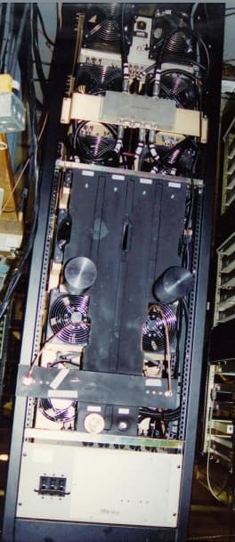
CJJ79XITS-7036
Mar 29, 2000MMDS/ITFS BROADBAND TRANSLATOR
Equipment Class
AMP - Amplifier